EP1092984A2 - Squid - Google Patents
Squid Download PDFInfo
- Publication number
- EP1092984A2 EP1092984A2 EP00402826A EP00402826A EP1092984A2 EP 1092984 A2 EP1092984 A2 EP 1092984A2 EP 00402826 A EP00402826 A EP 00402826A EP 00402826 A EP00402826 A EP 00402826A EP 1092984 A2 EP1092984 A2 EP 1092984A2
- Authority
- EP
- European Patent Office
- Prior art keywords
- squid
- thin film
- superconducting thin
- sapphire substrate
- film pattern
- Prior art date
- Legal status (The legal status is an assumption and is not a legal conclusion. Google has not performed a legal analysis and makes no representation as to the accuracy of the status listed.)
- Withdrawn
Links
- 241000238366 Cephalopoda Species 0.000 title claims abstract description 13
- 239000010409 thin film Substances 0.000 claims abstract description 83
- 239000000758 substrate Substances 0.000 claims abstract description 55
- 229910052594 sapphire Inorganic materials 0.000 claims abstract description 39
- 239000010980 sapphire Substances 0.000 claims abstract description 39
- CETPSERCERDGAM-UHFFFAOYSA-N ceric oxide Chemical compound O=[Ce]=O CETPSERCERDGAM-UHFFFAOYSA-N 0.000 claims abstract description 24
- 229910000422 cerium(IV) oxide Inorganic materials 0.000 claims abstract description 24
- 239000002887 superconductor Substances 0.000 claims description 3
- IJGRMHOSHXDMSA-UHFFFAOYSA-N Atomic nitrogen Chemical compound N#N IJGRMHOSHXDMSA-UHFFFAOYSA-N 0.000 description 18
- 238000000034 method Methods 0.000 description 13
- 230000000052 comparative effect Effects 0.000 description 9
- 239000007788 liquid Substances 0.000 description 9
- 238000004519 manufacturing process Methods 0.000 description 9
- 229910052757 nitrogen Inorganic materials 0.000 description 9
- 239000013078 crystal Substances 0.000 description 5
- 229910002370 SrTiO3 Inorganic materials 0.000 description 4
- 238000002474 experimental method Methods 0.000 description 3
- 239000000463 material Substances 0.000 description 3
- 230000000694 effects Effects 0.000 description 2
- 238000012986 modification Methods 0.000 description 2
- 230000004048 modification Effects 0.000 description 2
- 238000000206 photolithography Methods 0.000 description 2
- 230000035945 sensitivity Effects 0.000 description 2
- 229910000420 cerium oxide Inorganic materials 0.000 description 1
- 230000008859 change Effects 0.000 description 1
- 230000007423 decrease Effects 0.000 description 1
- 230000008021 deposition Effects 0.000 description 1
- 238000001514 detection method Methods 0.000 description 1
- 238000005530 etching Methods 0.000 description 1
- 239000010408 film Substances 0.000 description 1
- 230000004907 flux Effects 0.000 description 1
- BMMGVYCKOGBVEV-UHFFFAOYSA-N oxo(oxoceriooxy)cerium Chemical compound [Ce]=O.O=[Ce]=O BMMGVYCKOGBVEV-UHFFFAOYSA-N 0.000 description 1
- 238000000059 patterning Methods 0.000 description 1
- 230000009467 reduction Effects 0.000 description 1
- 238000000992 sputter etching Methods 0.000 description 1
Images

Classifications
-
- G—PHYSICS
- G01—MEASURING; TESTING
- G01R—MEASURING ELECTRIC VARIABLES; MEASURING MAGNETIC VARIABLES
- G01R33/00—Arrangements or instruments for measuring magnetic variables
- G01R33/02—Measuring direction or magnitude of magnetic fields or magnetic flux
- G01R33/035—Measuring direction or magnitude of magnetic fields or magnetic flux using superconductive devices
- G01R33/0354—SQUIDS
-
- H—ELECTRICITY
- H10—SEMICONDUCTOR DEVICES; ELECTRIC SOLID-STATE DEVICES NOT OTHERWISE PROVIDED FOR
- H10N—ELECTRIC SOLID-STATE DEVICES NOT OTHERWISE PROVIDED FOR
- H10N60/00—Superconducting devices
- H10N60/10—Junction-based devices
- H10N60/12—Josephson-effect devices
- H10N60/124—Josephson-effect devices comprising high-Tc ceramic materials
-
- H—ELECTRICITY
- H10—SEMICONDUCTOR DEVICES; ELECTRIC SOLID-STATE DEVICES NOT OTHERWISE PROVIDED FOR
- H10N—ELECTRIC SOLID-STATE DEVICES NOT OTHERWISE PROVIDED FOR
- H10N60/00—Superconducting devices
- H10N60/80—Constructional details
- H10N60/85—Superconducting active materials
- H10N60/855—Ceramic superconductors
- H10N60/857—Ceramic superconductors comprising copper oxide
Definitions
- the present invention relates to a SQUID (Superconducting QUantum Interference Device).
- a SQUID is constructed by forming at least one Josephson junction in a superconducting loop and used for an element such as a magnetometer capable of accurately measuring a magnetic field or a gradiometer.
- Some types of Josephson junctions are used in superconducting loops, and one of them is a step-edge Josephson junction.
- a step having a predetermined shape is formed on a substrate on which a superconducting loop is to be formed by a superconducting thin film pattern.
- a superconducting thin film pattern is formed on the substrate such that the step crosses a predetermined portion of the superconducting loop by a superconducting thin film.
- a Josephson junction is obtained using a weak link formed at the superconducting thin film pattern portion on the step.
- an SrTiO 3 substrate is generally used as a substrate because a satisfactory oxide superconducting thin film can be formed (Jpn. J. Appl. Phys., Vol. 32 (1993), pp. 662 - 664).
- an SrTiO 3 substrate is expensive, and a large SrTiO 3 substrate is unavailable. Since the number of SQUIDs which can be manufactured from a single wafer substrate decreases, the manufacturing efficiency is low.
- the area of a SQUID may be required to be large by, e.g., making the SQUID size large to increase the flux capture area.
- the above-described SQUID can hardly cope with an increase in area.
- the present invention has been made to solve the above-described problems, and has as its object to provide a SQUID which has a step-edge Josephson junction and is capable of attaining cost reduction and large area of the element.
- a SQUID comprising a sapphire substrate, and a superconducting thin film pattern formed from an oxide superconducting thin film formed on the sapphire substrate via a CeO 2 buffer layer and including a SQUID pattern, wherein a Josephson junction included in the SQUID pattern comprises a step-edge Josephson junction formed on a step on the sapphire substrate.
- the sapphire substrate used in the above SQUID is relatively inexpensive, and the substrate size can be made large.
- a technique of manufacturing a SQUID by forming a step-edge Josephson junction in forming a superconducting thin film pattern on a sapphire substrate has not been established.
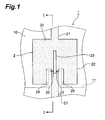
- Fig. 1 is a plan view showing a SQUID according to an embodiment of the present invention.
- Fig. 1 shows an enlarged view of a range including a superconducting thin film pattern portion where a SQUID pattern is formed in the SQUID, and the remaining thin film patterns are not illustrated.
- a SQUID 1 has a sapphire substrate 10 and a superconducting thin film pattern 20 formed on the sapphire substrate 10. On the sapphire substrate 10, a step having a predetermined angle and height is formed along a dashed line 11 shown in Fig. 1.
- the superconducting thin film pattern 20 has a thin film pattern 21 extending in the vertical direction in Fig. 1, and a square thin film pattern 22 having an outer size of 5 mm ⁇ 5 mm and formed at a predetermined position on the thin film pattern 21.
- a 5- ⁇ m wide, 100- ⁇ m long opening portion 23 is formed at the central portion of the thin film pattern 22 along the direction in which thin film pattern 21 extends.
- concave pattern portions 24 and 25 are formed at predetermined positions on the left and right sides of the thin film pattern 21 connected to the thin film pattern 22.
- the step 11 on the sapphire substrate 10 is formed along a line that crosses the thin film pattern 22 between the concave pattern portions 24 and 25 so as to pass through regions in the concave pattern portions 24 and 25 where the superconducting thin film pattern 20 is not formed and also pass through a position in the opening portion 23.
- the step 11 crosses a thin film pattern portion sandwiched between the right side of the concave pattern portion 24 and the left side of the opening portion 23 and a thin film pattern portion sandwiched between the left side of the concave pattern portion 25 and the right side of the opening portion 23.
- step-edge Josephson junctions are formed at two portions 26 and 27 crossed by the step 11, respectively.
- a SQUID pattern 2 included in the superconducting thin film pattern 20 of this embodiment is constructed by the above-described square thin film pattern 22, opening portion 23, and step-edge Josephson junctions 26 and 27.
- Fig. 2 is a sectional view of the SQUID shown in Fig. 1, which is taken along an arrow I - I therein.
- Fig. 2 shows an enlarged view of a sectional structure near the step-edge Josephson junction 26.
- the superconducting thin film pattern 20 of this embodiment is formed by sequentially forming a buffer layer 12 formed from a CeO 2 (cerium oxide) thin film and an oxide superconducting thin film 13 on the sapphire substrate 10.
- the sapphire substrate 10 also has the step 11 having a predetermined step angle ⁇ and step height h, as shown in Fig. 2.
- the step-edge Josephson junction 26 is obtained, as described above. More specifically, when the step 11 crosses the superconducting thin film pattern 20 formed from the oxide superconducting thin film 13 via the CeO 2 buffer layer 12, weak link is formed at the superconducting thin film portion which covers the step 11 whereby the step-edge Josephson junction 26 is obtained.
- the step angle ⁇ and step height h of the step 11 are the same for the step-edge Josephson junctions 26 and 27.
- the sapphire substrate 10 is used for a SQUID having a step-edge Josephson junction using a thin film pattern of an oxide superconductor.
- the sapphire substrate is relatively inexpensive, and a large sapphire substrate is available.
- the CeO 2 buffer layer 12 and oxide superconducting thin film 13 are sequentially formed on the sapphire substrate 10, thereby forming the superconducting thin film pattern 20.
- a SQUID can be obtained, in which a step-edge Josephson junction that enables the SQUID operation of the element is formed at a portion where the step 11 on the sapphire substrate 10 crosses the superconducting thin film pattern 20.
- a technique of forming an oxide superconducting thin film on a normal sapphire substrate via a CeO 2 buffer layer is described in, e.g., J. Appl. Phys. 70 (1991), pp. 3986 - 3988.
- a step-edge Josephson junction is formed using a structure in which an oxide superconducting thin film is formed on a sapphire substrate via a CeO 2 buffer layer, thereby reducing the cost of SQUID.
- the area of the SQUID can be increased, and the manufacturing efficiency can be improved.
- the crystal state and characteristics of the oxide superconducting thin film forming the superconducting thin film pattern are improved, thereby obtaining a SQUID capable of achieving a satisfactory superconducting characteristic and SQUID operation.
- an HoBaCuO-based oxide superconductor such as a HoBa 2 Cu 3 O 7-x thin film is preferably used. With this material, a superconducting thin film pattern having especially satisfactory crystal state and characteristics can be formed.
- the step angle ⁇ of the step 11 is preferably from 15° inclusive to 45° exclusive, and the step height h is preferably 100 nm to 600 nm both inclusive.
- the thickness of the CeO 2 buffer layer 12 is preferably from 10 nm inclusive to 60 nm exclusive.
- the thickness of the oxide superconducting thin film 13 is preferably 100 nm to 300 nm both inclusive.
- the characteristics of the SQUID can be particularly improved.
- the characteristics and preferable structural conditions of the SQUID 1 according to the above-described embodiment will be described below in more detail on the basis of examples and comparative examples.
- the structures of the superconducting thin film pattern 20 and SQUID pattern 2 formed at part of the superconducting thin film pattern 20 in the examples and comparative examples are the same as those in Figs. 1 and 2.
- a step 11 was formed on a sapphire substrate 10 by photolithography and ion milling etching.
- a CeO 2 buffer layer 12 and oxide superconducting thin film 13 formed from HoBa 2 Cu 3 O 7-x were sequentially formed on the substrate 10 by laser deposition, as shown in Fig. 2.
- the thickness of the CeO 2 buffer layer 12 was 30 nm, and the thickness of the HoBa 2 Cu 3 O 7-x thin film 13 was 120 nm.
- a superconducting thin film pattern 20 shown in Fig. 1, including a SQUID pattern 2 was formed by patterning using photolithography.
- the width of step-edge Josephson junctions 26 and 27 was 3 ⁇ m.
- the SQUID inductance was 30 pH.
- a SQUID was manufactured following the same procedures as in Example 1.
- a SQUID was manufactured following the same procedures as in Example 1.
- a SQUID was manufactured following the same procedures as in Example 1.
- the thickness of the CeO 2 buffer layer was 10 nm.
- a SQUID was manufactured following the same procedures as in Example 1.
- the thickness of the CeO 2 buffer layer was 55 nm.
- a SQUID was manufactured following the same procedures as in Example 1.
- the resultant SQUID was dipped in liquid nitrogen, and its characteristics were measured.
- the critical current value exceeded 1 mA to disable the SQUID operation.
- a SQUID was manufactured following the same procedures as in Example 1.
- the resultant SQUID was dipped in liquid nitrogen, and its characteristics were measured.
- the critical current value was 0, and no superconducting characteristic was exhibited to disable the SQUID operation.
- a SQUID was manufactured following the same procedures as in Example 1.
- the thickness of the CeO 2 buffer layer was 9 nm.
- the HoBa 2 Cu 3 O 7-x thin film was not satisfactorily grown on the step.
- the resultant SQUID was dipped in liquid nitrogen, and its characteristics were measured. No superconducting characteristic was exhibited to disable the SQUID operation.
- a SQUID was manufactured following the same procedures as in Example 1.
- the thickness of the CeO 2 buffer layer was 60 nm.
- the smoothness of the CeO 2 buffer layer surface was poor, and the HoBa 2 Cu 3 O 7-x thin film was not satisfactorily grown as a whole.
- the resultant SQUID was dipped in liquid nitrogen, and its characteristics were measured. No superconducting characteristic was exhibited to disable the SQUID operation.
- the shape of the step 11 to be formed on the sapphire substrate 10 and the thicknesses of the CeO 2 buffer layer 12 and oxide superconducting thin film 13 are preferably set within the preferable numerical ranges described in the above embodiment to form a step-edge Josephson junction such that sufficient characteristics are obtained.
- oxide superconducting thin film 13 another oxide high-temperature superconducting material may be used in place of the HoBa 2 Cu 3 O 7-x thin film.
- preferable numerical ranges of the structural conditions such as the angle and film thickness may change depending on the superconducting material used, the pattern shape such as the width of Josephson junction, or correlation between the structural conditions.
- preferable structural conditions for the manufacture of a SQUID are preferably determined on the basis of the structure of each SQUID.
- the SQUID according to the present invention has the following effects.
- a sapphire substrate is used as a substrate on which a thin film pattern of an oxide superconducting thin film is to be formed.
- the sapphire substrate is relatively inexpensive and available.
- the SQUID can be made inexpensive. Since a large sapphire substrate can be used, the number of SQUIDS which can be manufactured from a single wafer substrate can be increased to improve the manufacturing efficiency. The size of a SQUID to be manufactured can be large.
- a CeO 2 thin film is used as a buffer layer for the oxide superconducting thin film. This improves the crystal state and characteristics of the oxide superconducting thin film and makes it possible to obtain a step-edge Josephson junction that has satisfactory characteristics and enables the SQUID operation.
- the degree of freedom for the structure of the SQUID to be manufactured can be increased.
- SQUIDs having various application purposes and performances can be manufactured, so a SQUID having excellent performance, e.g., a SQUID magnetometer having an improved magnetic field sensitivity can be obtained.
Landscapes
- Physics & Mathematics (AREA)
- Chemical & Material Sciences (AREA)
- Engineering & Computer Science (AREA)
- Ceramic Engineering (AREA)
- Condensed Matter Physics & Semiconductors (AREA)
- General Physics & Mathematics (AREA)
- Superconductor Devices And Manufacturing Methods Thereof (AREA)
- Measuring Magnetic Variables (AREA)
Applications Claiming Priority (2)
| Application Number | Priority Date | Filing Date | Title |
|---|---|---|---|
| JP28975199 | 1999-10-12 | ||
| JP28975199A JP2001111123A (ja) | 1999-10-12 | 1999-10-12 | Squid素子 |
Publications (2)
| Publication Number | Publication Date |
|---|---|
| EP1092984A2 true EP1092984A2 (de) | 2001-04-18 |
| EP1092984A3 EP1092984A3 (de) | 2009-08-05 |
Family
ID=17747301
Family Applications (1)
| Application Number | Title | Priority Date | Filing Date |
|---|---|---|---|
| EP00402826A Withdrawn EP1092984A3 (de) | 1999-10-12 | 2000-10-12 | Squid |
Country Status (5)
| Country | Link |
|---|---|
| US (1) | US6384424B1 (de) |
| EP (1) | EP1092984A3 (de) |
| JP (1) | JP2001111123A (de) |
| KR (1) | KR20010050950A (de) |
| CA (1) | CA2323128A1 (de) |
Families Citing this family (11)
| Publication number | Priority date | Publication date | Assignee | Title |
|---|---|---|---|---|
| JP4132720B2 (ja) * | 2001-05-07 | 2008-08-13 | 独立行政法人科学技術振興機構 | 量子干渉型磁束計の製造方法 |
| US20030068832A1 (en) * | 2001-08-29 | 2003-04-10 | Yuri Koval | Submicron closed-form josephson junctions |
| US9768371B2 (en) | 2012-03-08 | 2017-09-19 | D-Wave Systems Inc. | Systems and methods for fabrication of superconducting integrated circuits |
| WO2013149607A1 (de) * | 2012-04-04 | 2013-10-10 | Forschungszentrum Jülich GmbH | Reproduzierbarerer stufen-josephson-kontakt |
| WO2018144601A1 (en) | 2017-02-01 | 2018-08-09 | D-Wave Systems Inc. | Systems and methods for fabrication of superconducting integrated circuits |
| WO2019117929A1 (en) * | 2017-12-15 | 2019-06-20 | Intel Corporation | Wafer-scale manufacturing of josephson junctions for qubits |
| US20200152851A1 (en) | 2018-11-13 | 2020-05-14 | D-Wave Systems Inc. | Systems and methods for fabricating superconducting integrated circuits |
| US12102017B2 (en) | 2019-02-15 | 2024-09-24 | D-Wave Systems Inc. | Kinetic inductance for couplers and compact qubits |
| JP7705393B2 (ja) | 2019-12-05 | 2025-07-09 | ディー-ウェイブ システムズ インコーポレイテッド | 超伝導集積回路を製造するためのシステム及び方法 |
| WO2021231224A1 (en) | 2020-05-11 | 2021-11-18 | D-Wave Systems Inc. | Kinetic inductance devices, methods for fabricating kinetic inductance devices, and articles employing the same |
| US12392823B2 (en) | 2021-11-05 | 2025-08-19 | D-Wave Systems Inc. | Systems and methods for on-chip noise measurements |
Family Cites Families (6)
| Publication number | Priority date | Publication date | Assignee | Title |
|---|---|---|---|---|
| DE4212028C2 (de) * | 1991-05-08 | 1994-06-16 | Siemens Ag | Korngrenzen-Josephsonelement mit metalloxidischem Hochtemperatursupraleiter-Material, Verfahren zu dessen Herstellung sowie Verwendung des Elementes |
| EP0660968A1 (de) * | 1992-09-14 | 1995-07-05 | Conductus, Inc. | Verbesserte sperrschichten fuer oxid-supraleiter-anordnungen und schaltungen |
| US5567673A (en) * | 1994-10-17 | 1996-10-22 | E. I. Du Pont De Nemours And Company | Process of forming multilayered Tl-containing superconducting composites |
| AU7458796A (en) * | 1995-10-24 | 1997-05-15 | Regents Of The University Of California, The | High temperature superconducting josephson junctions and squids |
| US5742073A (en) * | 1996-09-27 | 1998-04-21 | The United States Of America As Represented By The Secretary Of The Air Force | Superconducting weak link array switch |
| JPH11274586A (ja) * | 1998-03-23 | 1999-10-08 | Sumitomo Electric Ind Ltd | サファイア基板を用いたsquidとその製造方法 |
-
1999
- 1999-10-12 JP JP28975199A patent/JP2001111123A/ja not_active Withdrawn
-
2000
- 2000-10-11 US US09/686,386 patent/US6384424B1/en not_active Expired - Fee Related
- 2000-10-11 KR KR1020000059697A patent/KR20010050950A/ko not_active Withdrawn
- 2000-10-11 CA CA002323128A patent/CA2323128A1/en not_active Abandoned
- 2000-10-12 EP EP00402826A patent/EP1092984A3/de not_active Withdrawn
Also Published As
| Publication number | Publication date |
|---|---|
| JP2001111123A (ja) | 2001-04-20 |
| US6384424B1 (en) | 2002-05-07 |
| EP1092984A3 (de) | 2009-08-05 |
| CA2323128A1 (en) | 2001-04-12 |
| KR20010050950A (ko) | 2001-06-25 |
Similar Documents
| Publication | Publication Date | Title |
|---|---|---|
| US5465049A (en) | Integrated type planar magnetic sensor having SQUID and flux transformer formed of oxide superconductor | |
| US7482804B2 (en) | Superconducting quantum interference device | |
| US5574290A (en) | Superconducting quantum interference device | |
| US6384424B1 (en) | Squid | |
| CN104350623B (zh) | 具有约瑟夫森触点的组件及其制造方法 | |
| EP0926508B1 (de) | Magnetsensor mit Supraleiter | |
| CA2037949C (en) | Stacked josephson junction device composed of oxide superconductor material | |
| EP0493258B1 (de) | Supraleitende Quanten-Interferenz-Einrichtung aus supraleitender oxydischer Dünnschicht | |
| JP2621623B2 (ja) | スクイド | |
| EP0573340A1 (de) | Josephson-Uebergangseinrichtung aus oxidischem Supraleiter | |
| CA2073831C (en) | Josephson junction device of oxide superconductor and process for preparing the same | |
| EP0566499B1 (de) | Planares Quanteninterferometer mit Oxid-Supraleiter | |
| JP4820481B2 (ja) | 超伝導量子干渉素子 | |
| EP0753757B1 (de) | Planarer magnetischer Sensor mit einem SQUID aus supraleitender Dünnschicht | |
| US5883051A (en) | High Tc superconducting Josephson junction element | |
| Seidel et al. | Development and investigation of novel single-layer gradiometers using highly balanced gradiometric SQUIDs | |
| EP0524862A1 (de) | Vorrichtung mit Josephson-Übergang aus supraleitendem Oxyd und Verfahren zu seiner Herstellung | |
| USRE37587E1 (en) | Superconducting quantum interference device formed of oxide superconductor thin film | |
| JPH05297093A (ja) | 磁気センサ | |
| US5612545A (en) | Superconducting quantum interference device formed of oxide superconductor thin film | |
| JP2943293B2 (ja) | Dc―squid磁力計 | |
| JPH0323684A (ja) | ジョセフソン接合素子 | |
| JPH04233286A (ja) | Squid素子 | |
| JP2000058932A (ja) | 磁気センサ及びグラジオメータ | |
| JPH02205785A (ja) | 超電導デバイス |
Legal Events
| Date | Code | Title | Description |
|---|---|---|---|
| PUAI | Public reference made under article 153(3) epc to a published international application that has entered the european phase |
Free format text: ORIGINAL CODE: 0009012 |
|
| AK | Designated contracting states |
Kind code of ref document: A2 Designated state(s): AT BE CH CY DE DK ES FI FR GB GR IE IT LI LU MC NL PT SE |
|
| AX | Request for extension of the european patent |
Free format text: AL;LT;LV;MK;RO;SI |
|
| PUAL | Search report despatched |
Free format text: ORIGINAL CODE: 0009013 |
|
| AK | Designated contracting states |
Kind code of ref document: A3 Designated state(s): AT BE CH CY DE DK ES FI FR GB GR IE IT LI LU MC NL PT SE |
|
| AX | Request for extension of the european patent |
Extension state: AL LT LV MK RO SI |
|
| AKX | Designation fees paid | ||
| STAA | Information on the status of an ep patent application or granted ep patent |
Free format text: STATUS: THE APPLICATION IS DEEMED TO BE WITHDRAWN |
|
| 18D | Application deemed to be withdrawn |
Effective date: 20100206 |
|
| REG | Reference to a national code |
Ref country code: DE Ref legal event code: 8566 |