EP1089436B1 - Current-mode spike-based analog-to-digital conversion - Google Patents
Current-mode spike-based analog-to-digital conversion Download PDFInfo
- Publication number
- EP1089436B1 EP1089436B1 EP00308110A EP00308110A EP1089436B1 EP 1089436 B1 EP1089436 B1 EP 1089436B1 EP 00308110 A EP00308110 A EP 00308110A EP 00308110 A EP00308110 A EP 00308110A EP 1089436 B1 EP1089436 B1 EP 1089436B1
- Authority
- EP
- European Patent Office
- Prior art keywords
- neuron
- circuit
- state
- analog
- neuron circuit
- Prior art date
- Legal status (The legal status is an assumption and is not a legal conclusion. Google has not performed a legal analysis and makes no representation as to the accuracy of the status listed.)
- Expired - Lifetime
Links
- 238000006243 chemical reaction Methods 0.000 title claims description 76
- 210000002569 neuron Anatomy 0.000 claims description 135
- 238000000034 method Methods 0.000 claims description 44
- 238000012421 spiking Methods 0.000 claims description 33
- 238000006073 displacement reaction Methods 0.000 claims description 9
- 238000009825 accumulation Methods 0.000 claims description 2
- 238000007670 refining Methods 0.000 claims 2
- 238000011156 evaluation Methods 0.000 description 37
- 230000007704 transition Effects 0.000 description 27
- 238000012937 correction Methods 0.000 description 26
- 239000003990 capacitor Substances 0.000 description 25
- 230000006870 function Effects 0.000 description 14
- 238000012545 processing Methods 0.000 description 13
- 230000001960 triggered effect Effects 0.000 description 13
- 238000013139 quantization Methods 0.000 description 9
- 230000008569 process Effects 0.000 description 8
- 230000008901 benefit Effects 0.000 description 5
- 238000013507 mapping Methods 0.000 description 5
- 230000001537 neural effect Effects 0.000 description 5
- 238000013461 design Methods 0.000 description 4
- 230000000694 effects Effects 0.000 description 4
- 238000010304 firing Methods 0.000 description 4
- 230000007246 mechanism Effects 0.000 description 4
- 230000003321 amplification Effects 0.000 description 3
- 230000008859 change Effects 0.000 description 3
- 230000010354 integration Effects 0.000 description 3
- 230000003993 interaction Effects 0.000 description 3
- 238000003199 nucleic acid amplification method Methods 0.000 description 3
- 230000004913 activation Effects 0.000 description 2
- 230000002411 adverse Effects 0.000 description 2
- 238000013459 approach Methods 0.000 description 2
- 230000005540 biological transmission Effects 0.000 description 2
- 230000015556 catabolic process Effects 0.000 description 2
- 238000006731 degradation reaction Methods 0.000 description 2
- 230000000593 degrading effect Effects 0.000 description 2
- 230000001419 dependent effect Effects 0.000 description 2
- 238000010586 diagram Methods 0.000 description 2
- 230000008520 organization Effects 0.000 description 2
- 238000003909 pattern recognition Methods 0.000 description 2
- 230000001360 synchronised effect Effects 0.000 description 2
- 241001465754 Metazoa Species 0.000 description 1
- 239000008186 active pharmaceutical agent Substances 0.000 description 1
- 238000013528 artificial neural network Methods 0.000 description 1
- 230000001143 conditioned effect Effects 0.000 description 1
- 238000005516 engineering process Methods 0.000 description 1
- 230000036039 immunity Effects 0.000 description 1
- 238000005259 measurement Methods 0.000 description 1
- 239000000203 mixture Substances 0.000 description 1
- 238000012986 modification Methods 0.000 description 1
- 230000004048 modification Effects 0.000 description 1
- 238000012805 post-processing Methods 0.000 description 1
- 230000002028 premature Effects 0.000 description 1
- 230000001902 propagating effect Effects 0.000 description 1
- 238000005070 sampling Methods 0.000 description 1
- 239000004065 semiconductor Substances 0.000 description 1
- 238000000926 separation method Methods 0.000 description 1
- 238000012360 testing method Methods 0.000 description 1
Images


Classifications
-
- H—ELECTRICITY
- H03—ELECTRONIC CIRCUITRY
- H03M—CODING; DECODING; CODE CONVERSION IN GENERAL
- H03M1/00—Analogue/digital conversion; Digital/analogue conversion
- H03M1/12—Analogue/digital converters
- H03M1/14—Conversion in steps with each step involving the same or a different conversion means and delivering more than one bit
- H03M1/16—Conversion in steps with each step involving the same or a different conversion means and delivering more than one bit with scale factor modification, i.e. by changing the amplification between the steps
- H03M1/164—Conversion in steps with each step involving the same or a different conversion means and delivering more than one bit with scale factor modification, i.e. by changing the amplification between the steps the steps being performed sequentially in series-connected stages
-
- H—ELECTRICITY
- H03—ELECTRONIC CIRCUITRY
- H03M—CODING; DECODING; CODE CONVERSION IN GENERAL
- H03M1/00—Analogue/digital conversion; Digital/analogue conversion
- H03M1/12—Analogue/digital converters
- H03M1/60—Analogue/digital converters with intermediate conversion to frequency of pulses
Definitions
- the present invention relates generally to the field of electronic computers and computation. More particularly, the present invention relates, in one aspect, to hybrid analog and digital computation. Still more particularly, the present invention relates to spike-based analog-to-digital conversion using hybrid analog-digital techniques and organizations.
- Analog-to-digital conversion is used in a wide variety of electronics applications -from testing and measurement to entertainment electronics and beyond.
- any electronics application that involves real-word (analog) signals such as sounds, light and temperature employs treatment of corresponding signals in digital form for some part of its operation.
- real-word signals such as sounds, light and temperature
- music compact discs store and make available for retrieval digital versions of what normally originate as analog voice or instrument signals. Upon retrieval, such stored signals typically return to their original analog form for playback.
- analog-to-digital (A/D) conversion relates to the conversion of a continuous variable to a nearest discrete approximation, which approximation is generally represented as a multi-bit binary number. See, for example, P. Horowitz and W. Hill, The Art of Electronics , Cambridge Univ. Press, Cambridge, 1989, pp. 612-641.
- A/D converters employ voltage sample-and-hold techniques. These prior techniques thus employ a voltage signal sampled at an instant within a longer period, rather than using a signal averaged over the period. In such sampled operation, noise present at the time of sampling can significantly affect the value used in conversion.
- US 5,420,963 discloses a signal processing apparatus using a neural network.
- a further aspect of the patent application entitled Spike-Based Hybrid Computation is the use in some cases of analog-to-digital conversion techniques, e.g ., in restoring analog signals to avoid significant degradation during transmission and processing over time. This restoration is convieniently performed as an analog-to-digital conversion followed by a digital-to-analog conversion.
- a simple digital-to-analog (D/A) converter is used to convert the A/D-converted value (from binary form) back to a continuous value - thus implementing an analog-to-digital-to-analog (A/D/A) conversion. It will be appreciated that such use of an A/D/A process effectively performs a rounding operation.
- A/D converter circuits and techniques are described that are useful when the input is a current and also prove useful in the context of spike-based computing of the type described above.
- Use of combined analog and digital circuitry employing spiking neuron signals contributes to high power and device implementation efficiencies.
- Present inventive circuits and techniques differ from prior A/D designs in several respects.
- present inventive contributions are charge-and-current based rather than voltage-based.
- input current is not sampled at an instant, but rather is represented by its average effect in an integration period, i.e ., by its charge-accumulation capabilities over time. Improved noise immunity is thereby realized.
- no explicit sample-and-hold (S / H) circuit is necessary in application of the present inventive techniques, because integration of input current for a given time period on a capacitor is used instead.
- input signals are sensed only at one stage of the computation; all further information is coded in successive residues.
- no explicit subtractor is required in the present inventive architecture; subtraction is performed implicitly by resetting of a neuron.
- DACs digital-to-analog converters
- present inventive architectures prove very area efficient for device implementation.
- Non-pipelined architectures are also used to advantage in embodiments of the present invention to further increase area efficiency, at least in part because coarse and fine conversions use the same 2-neuron circuit.
- the small number of circuit components that are required in illustrative embodiments increases the power efficiency as well. Power efficiency is further enhanced because charging currents need be present only when needed.
- the digital portions of our architecture such as a spike-triggered state machine used to coordinate operations, consume switching power only when spiking events trigger transitions.
- the phenomenon of metastability i.e., indecisive behavior between output '0' and '1' decisions in the converter, is avoided via the use of error correction of a large charge residue.
- Traditional A/D converters that perform voltage comparisons are prone to the adverse effects of metastability.
- Spike-based hybrid computation uses spikes (pulses) to compute in a fashion that is not purely analog or purely digital, but is a hybrid mixture of both forms of computation.
- spikes pulses
- this hybrid scheme uses several moderate-precision distributed analog units to collectively compute a precise answer to a computation; frequent discrete signal restoration of the analog information prevents analog noise and offset from degrading the computation.
- FIG. 2 shows illustrative capacitors 210 and 260 that serve to receive input charge. Each capacitor's state is advantageously changed by charging the capacitor with the sum of all its input currents ⁇ i I i . Unless otherwise mentioned, we will, for simplicity, also assume that all I t are positive, though no such restriction applies in the general case.
- the time period for integration of applied currents is taken as t tn , a period that is convieniently gated by a pulse input, or is ungated.
- every analog state variable will likely reach the upper limit of its dynamic range, e.g ., the power supply voltage - or a fraction of the power supply voltage. It proves convienient in many contexts to prevent this from occurring, as will be appreciated from the following discussion. So, a threshold level of charge, Q T , is selected, such that if Q state ⁇ Q T , charging continues. But, if Q state > Q T , the state variable is reset to 0, and a signal is sent to a neighboring channel indicating that we have performed a reset; charging then resumes.
- the signal sent to the neighboring channel takes the form of a spike signal of the form described, e.g.
- the channel to which the illustrative spike signal is sent advantageously includes a similar charge-and-reset unit on another nearby capacitor.
- the spike then causes the neighboring channel to increment its charge by a discrete amount that is typically a fraction of Q T .
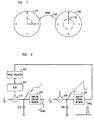
- FIG. 1 illustrates the charge-and-fire operation just described.
- a first circle 100 represents real numbers by their angular position of an arrow or vector 101 on the unit circle.
- the representation "wraps around” by resetting to 0, with the accompanying transmission of a spike (or other) signal 105 to the neighboring channel (represented by circle 110).
- the illustrative spike signal indicates that the preceding accumulate-and-fire circuit has caused the corresponding charge signal representation to perform one full revolution.
- the adjacent channel keeps track of the number of full revolutions performed at its neighbor circle 100, by a rotational increment at circle 110.
- the charge thus deposited on the capacitor corresponding to the angular displacement on circle 110 typically reflects a charge of less than Q T on that capacitor. This idea can be repeated ad infinitum , so that complete revolutions of the cited neighbor circle are accounted for by partial increments of yet another channel, and so on. It will be recognized that the approach just described overcomes limitations of the prior art regarding limited-dynamic-range for an analog variable.
- the above-described strategy represents information about a variable across many channels.
- the function ⁇ (x) is the Heaviside function which is 1', if x > 0 and 0 if x ⁇ 0.
- the function [x] is the floor function that rounds a real number to the nearest integer.
- the symbol ⁇ represents an angular frequency that is determined by the sum of the charging currents.
- One way of preserving the 2-bit representation across channels in is to increment the neighboring channel by ⁇ /2 whenever the current channel has finished a full revolution of 2 ⁇ .
- Such a scheme is illustrated in FIG. 2, where we charge the neighboring channel (the capacitor 210) by 1 unit when the current channel (capacitor 260) has completed a full revolution of 4 units.
- full revolutions of a neighbor result in a quarter-revolution increments of yet another neighbor to the left of it, and so on, a method is provided for approximating an analog number in a number representation based on radix 4.
- each of the channels of the described distributed number representation may also have its own analog input currents that arise from a source other than the immediate neighbor to their right.
- spiking outputs from spiking neuron circuit 250 reflecting a full charge on capacitor 260 (2 ⁇ rotation of its corresponding vector) are applied by connection to the neighboring channel to create an incremental charge on capacitor 210 for that neighboring channel vector.
- the spiking signal from neuron circuit 250 advantageously is applied to current summer through a spike counter 220 and a (simple) digital-to-analog converter 225.
- an arriving spiking pulse can gate a standard charging current to the neighboring capacitor.
- This charging current may be chosen such that the charge is incremented by one unit.
- Such a scheme can be implemented using well-known circuit design techniques with as few as two transistors in series (one for gating and one for the current source). Any accumulated offsets due to mismatches in the current sources are irrelevant so long as we ensure that the sum of all these offsets is less than half the separation between discrete attractor levels prior to the roundoff operation.
- input currents I 2 / tn other than the inter-channel spiking input from neuron circuit 250 are applied to charge a capacitor.
- the capacitor has received the threshold amount of charge (the capacitor has reached a corresponding threshold voltage) it fires a spike via a spiking neuron circuit.
- the inputs such as I 2 / tn shown in FIG. 2 represent analog input currents to the respective channel for charging the respective channel capacitor to reflect signal conditions other than the spiking input from a neighboring channel.
- HSMs hybrid state machines
- Hybrid state machines possess both discrete digital states and continuous analog states, next-state functions for discrete and continuous states, analog and digital output functions, and interaction functions that define the interactions between the machine's analog and digital parts.
- no clock is required - all transitions are triggered by spiking events.
- Illustrative spiking circuits and signals are described in my patent application entitled Spiking Neuron Circuit . It will be appreciated that traditional finite-state machines are a special case of hybrid state machines with only digital inputs, with only discrete states, and with only one special input (the clock) that is capable of triggering transitions between states.
- FIG. 3 shows the architecture of an illustrative hybrid state machine.
- the machine is shown comprising two principal parts: (i) an analog part 320 with analog states (illustratively encoded on a set of capacitor charge variables), and with analog inputs and outputs AI and AO on leads 321 and 322, respectively; and (ii) a digital part 310 with discrete states DS encoded on a set of register variables stored in register 315 and having digital inputs and outputs DI and DO on leads 311 and 312, respectively.
- Analog part 320 also comprises analog processing element (s) 327, while digital part 310 further comprises combination logic 317.
- digital part 310 may alter the values of a set of binary outputs (binary control vector, 330) to control switches in the analog part 320, consequently affecting the analog system's operation.
- analog part 320 generates spiking events as an output spike vector, Sp , which triggers transitions between discrete states in digital part 310.
- Digital control of the analog part 320 of the hybrid state machine of FIG. 3 may be exercised in at least three ways.
- D/A converters DACs
- DACs D/A converters
- a current equal to 4 I 0 will illustratively be created by switching particular control bits supplied to a DAC to the bit pattern 100.
- This 4 I 0 current then changes the state of a capacitor in analog system 320 for which this current is a charging input.
- Any analog parameters such as thresholds, pulse widths, charging currents, capacitance values etc. may be altered this way.
- digital control bits alter the parameters of analog system 320 by setting selected analog parameters to zero while enabling other analog parameters to express their value.
- an analog input current, I tn from outside the hybrid state machine may be allowed to assume its value during a sensing operation or it may be effectively set to zero, depending on the state of a specified control bit.
- digital control bits may reconfigure an analog topology by turning on or off particular switches included in analog processing unit 327 in analog portion 320. For example, an operational amplifier that is present in the analog system may be disconnected from the rest of the system when a particular digital control bit is 1.
- Control by analog part 320 of digital part 310 is effected by having particular spikes or particular spiking patterns trigger transitions between the discrete states.
- arbitrary spiking patterns may be recognized by a hybrid state machine that has all its transitions triggered by the arrival of a particular spike.
- the particular spike used to effect this transition may differ from state to state, but any given transition is always caused by one spike.
- This spike-pattern-recognition machine may be embedded within a larger hybrid state machine and have the spike-pattern-recognition machine generate a spike when the appropriate spiking pattern is recognized.
- all hybrid state machines make transitions based on only a single triggering spike.
- transitions between discrete states may be conditioned on a spike arrival as well as on the states of other digital inputs.
- the digital portion of a hybrid state machine (styled a spike-triggered finite state machine ) is described in detail in my patent application filed on the same day as the present application and entitled A Spike-Triggered Asynchronous Finite State Machine .
- Nonvolatile analog memory Because robust nonvolatile analog memory is difficult to realize in practice, we will generally assume that analog states are volatile and destructible, at least over a long time scale. Nonvolatile digital state is easily realized using such devices as SRAMs. Thus, if it is important to store analog state variables over a time scale that is much longer than the typical leak time of capacitors used in analog part 320, it will prove convienient to perform analog-to-digital conversion to the precision needed and store the analog state digitally. Such conversion will be described more fully below.
- a hybrid state machine for performing A/D conversion is readily embedded within a larger hybrid state machine.
- it proves convienient to transition from states of the larger machine to states of the conversion machine when we wish to perform analog-to-digital conversion, and then return to the large machine when we complete the conversion.
- we have effectively created an analog-to-digital-conversion "subroutine" that we call from a larger (hybrid state machine) program.
- Certain changes in discrete states in digital part 310 of the hybrid state machine of FIG. 3 may result in no changes in analog part 320.
- counting spikes in a particular phase of A/D conversion alters the discrete states of a counter - but does not affect any analog parameters.
- Analog parameters advantageously change only after a transition to another phase of operation; such a transition is illustratively triggered by spikes that are not related to the spikes counted in the prior phase of operation.
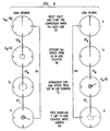
- FIG. 4A shows the angular state variables of 2 spiking neurons, called the timing neuron (TN) and counting neuron (CN) respectively.
- the charging rate of CN is 4 times that of the charging rate of TN . If we stop charging both neurons as soon as TN spikes, i.e.
- CN will make n full revolutions and fire n spikes in the time that it takes TN to fire 1 spike, by counting the number of spikes that CN fires, we may evaluate ⁇ rounded down to the nearest whole multiple of ⁇ /2.
- the arrow in FIG. 4A is labeled Sp TN to indicate that a state transition occurs at the onset of this spike.
- the charging currents to the neurons are altered; in FIG. 4A and FIG. 4B, after the state transition, the charging currents to both neurons are 0, but, in general, the charging currents could be altered to values dictated by subsequent processing.
- the charging currents for each neuron in a given state are labeled alongside the diagrammatic representation of their state variables at the beginning of the state.
- FIG. 4B shows the same two neurons, but with the angular state variable of TN initially at + ⁇ rather than - ⁇ .
- This case is equivalent to the case discussed with reference to FIG. 4A except that the multiply-by-4 operation is on 2 ⁇ - ⁇ rather than on ⁇ .
- the number of spikes fired by CN in the time that TN takes to fire one spike is 3 - n .
- Eq. (6) shows that when we do a downcounting evaluation of ⁇ we are left with a residue 2 ⁇ -4 ⁇ . This residue is in a form suitable for further evaluation by upcounting.
- Eq. (5) shows that when we do an upcounting evaluation of ⁇ we are left with a residue 4 ⁇ . This residue is in a form suitable for further evaluation by downcounting.
- the techniques of upcounting and downcounting enable us to do a coarse evaluation of ⁇ to the nearest whole multiple of ⁇ /2, leaving a residue for finer evaluation in a subsequent stage of processing:
- the [0, ⁇ /2] range of ⁇ is amplified to [0, 2 ⁇ ) for the fine stage evaluation.
- By successively alternating upcounting and downcounting evaluations we may get finer and finer estimates of ⁇ . These successive evaluations form a basis of the analog-to-digital conversion technique described in detail below.
- FIG. 5 shows how we perform error correction in an architecture where the last stage of the conversion involves downcounting; extension of the technique to an architecture where the last stage of the conversion involves upcounting is straightforward.
- n we only change our estimate of n when an odd number of spikes has been fired. If no spikes are fired, we interpret n to be 4; generating a carry to an adjacent channel usually represents the value of 4.
- the compressive nature of the mapping (more than one value in the number of spikes fired results in the same n ) provides error correction, i.e ., rounding of n to its nearest value such that the LSB is evaluated correctly.
- the tabular mapping of Table 1 is easily implemented by reading the 1st and 2nd most significant bits of a 3-bit spike-triggered counter that has been initialized to 000. We downcount as each n ' spike arrives; a simple circuit generates an overflow carry to represent 4 in an adjacent channel in the absence of any spike arrivals.
- the tabular mapping of Table 2 is easily implemented by reading the 1st and 2nd most significant bits of a 3-bit spike-triggered counter that has been initialized to 001. We upcount as each n ' spike arrives. In a manner similar to the downcounting arrangement, a 00 in the 2 most significant bits of the counter and the presence of at least one spike arrival generate an overflow carry. Upcounting Error Correction Spikes Fired n 0 0 1,2 1 3,5 2 5,6 3 7,8 4
- FIG. 6 shows an architecture for a 2-step A/D converter.
- the converter first performs a 2-bit coarse quantization followed by a 2-bit fine quantization of the residue from the coarse quantization.
- the architecture comprises two neurons whose states and charging currents evolve during the process of conversion as shown in FIG. 6. There are 4 discrete states in the conversion process, in each of which there is a different configuration of charging currents for the two neurons. In FIG. 6 the state of each neuron at the beginning of the discrete state, and the charging currents for the 2 neurons in each state are indicated.
- the discrete states, and spike-triggered transitions required of A/D conversion are implemented with a spike-triggered finite state machine; the machine's outputs control the configuration of charging currents to the neurons.
- An illustrative finite-state machine for use in this context is described in the patent application entitled A Spike-Triggered Asynchronous Finite State Machine .
- the combination of the several illustrative spike-based analog circuits (such as the 2-step A/D converter just described) with spike-triggered finite state machines falls within the broad category of hybrid state machine as note above and described in detail in the patent application entitled Spike-Based Hybrid Computation.
- FIG. 7 shows an A/D architecture that we term a successive subranging architecture.
- a pipelined version of this architecture is described below.
- a quantization is performed, and the residue is amplified and input to the next stage of processing where the process repeats again.
- We may think of this process as viewing the residue at successively higher magnifications.
- At each magnification we extract an integer measure of the residue and amplify the residual fraction for the next stage to evaluate.
- Eq. (6) shows that downcounting results in an integer evaluation of 3 - n , and a fractional residue that is amplified by 4 and in a form that is exactly suited for finer evaluation by an upcounting stage.
- the finer evaluation results because we map ⁇ , which exists in a [0, ⁇ /2] range, to a [0, 2 ⁇ ] range.
- the fractional residue is in the form 2 ⁇ - 4 ⁇ which allows us to perform a direct evaluation of 4 ⁇ in an upcounting stage.
- Eq. (5) shows that upcounting results in an integer evaluation of n , and a fractional residue that is amplified by 4 and in a form that is exactly suited for finer evaluation by an downcounting stage.
- the finer evaluation results because we map ⁇ , which exists in a [0, ⁇ /2] range, to a [0, 2 ⁇ ] range.
- the fractional residue is in the form 4 ⁇ , which allows us to perform a direct evaluation of 4 ⁇ in a downcounting stage.
- FIG. 7 illustrates the details of the architecture which is implemented with two spiking neuron circuits, neuron A and neuron B, and is composed of four discrete states.
- incrementing the final 2-bit LSB counter during error correction can cause the incrementing carry to propagate through to the other more significant 2-bit counters; these counters may be viewed as being chained together to create a global counter that represents the answer of the conversion.
- FIG. 8 shows how we may construct an 8-bit pipelined successive-subranging converter.
- the T-neurons control the evaluation period of the neighboring E-neuron to their right by determining this E-neuron's time period of charging.
- the E-neurons generate upcounting/downcounting spikes and create a residue by amplification of the T-neuron's residue.
- the first E-neuron in the cascade creates a residue, not via amplification, but via charging from the input current.
- Any E-neuron at a given location always upcounts/downcounts (or doesn't count if its the 2nd neuron during input charging), and there is an alternation of upcounting/downcounting stages.
- we enter a mode of operation where the T-neurons become E-neurons, and the E-neurons become T-neurons.
- the two rows of FIG. 8 illustrate the two configurations that the A/D converter is constantly alternating between. The residue is thus asynchronously evaluated, amplified, and passed amongst the neurons from left to right in a pipelined fashion.
- the first neuron in the cascade of FIG. 8 is used to time the generation of the input residue on its neighbor. It behaves as a T-neuron when it performs this function, and is inactive (zero charging current) when it is an E-neuron.
- the very last neuron in the cascade performs the final error correction and evaluation. It behaves as an E-neuron when it performs this function, and is inactive when it is a T-neuron.
- the stages to the left in FIG. 8 are simultaneously processing new inputs while the stages to the right are processing old ones.
- this may be readily accomplished by alternating the T and E modes of each neuron on two phases of a clock.
- the outputs of the counters in this synchronous mode are latched in registers that alternate between write-mode when the corresponding neuron is in E -mode, and hold-mode when the corresponding neuron is in T -mode.
- This section describes an example 4-bit A/D converter in the form of a semiconductor chip that may illustratively be built using a 0.5 ⁇ m HP MOSIS process with a 3.3V power-supply voltage.
- the converter obtains its 2 most significant bits via an overranging step, and its 2 least significant bits via a 2-bit residue-evaluation and error-correction step.
- the flow diagram for the evolution of the converter is shown in FIG. 9. There are four discrete states and two neurons labeled the MSBs-neuron and LSBs-neuron respectively.
- FIG. 10 shows the clock Phi, MSBs-neuron, and LSBs-neuron state variables during a full cycle of conversion.
- the LSBs neuron fires 2 spikes while the MSBs neuron fires 1 spike.
- the most significant bits are evaluated as 10.
- the residue left on the LSBs neuron is evaluated by the MSBs neuron to be 10: From Table 2, the 4 spikes fired by the MSBs neuron during SL correspond to a rounded value of 2.
- I tn ( I 0 /4) ⁇ (10.10), or, more simply I tn ⁇ 2.5(I 0 /4).
- FIG. 11 shows that the B 3 B 2 B 1 B 0 state of the MSBs and LSBs counter conglomerate is indeed 1010 at the end of the conversion.
- FIG. 12 shows the SM, SL, SW and SD logical state variables during the conversion; the logical combination (SW OR SD) is also shown.
- FIG. 13 shows the spikes Sp M and Sp L fired by the MSBs and LSBs neurons during conversion.
- the very first spike fired by the MSBs-neuron causes the quick transition out of SD and into SM.
- the LSBs neuron fires 2 spikes.
- the second spike on the MSBs neuron causes a transition out of SM and into SL.
- the remaining four spikes on the MSBs-neuron are fired during SL.
- the SL state concludes when the LSBs-neuron fires its timing spike, the last spike of the LSBs neuron in FIG. 13.
Landscapes
- Engineering & Computer Science (AREA)
- Theoretical Computer Science (AREA)
- Analogue/Digital Conversion (AREA)
Applications Claiming Priority (2)
| Application Number | Priority Date | Filing Date | Title |
|---|---|---|---|
| US408379 | 1999-09-29 | ||
| US09/408,379 US6262678B1 (en) | 1999-09-29 | 1999-09-29 | Current-mode spike-based analog-to-digital conversion |
Publications (3)
| Publication Number | Publication Date |
|---|---|
| EP1089436A2 EP1089436A2 (en) | 2001-04-04 |
| EP1089436A3 EP1089436A3 (en) | 2004-01-02 |
| EP1089436B1 true EP1089436B1 (en) | 2005-11-16 |
Family
ID=23616058
Family Applications (1)
| Application Number | Title | Priority Date | Filing Date |
|---|---|---|---|
| EP00308110A Expired - Lifetime EP1089436B1 (en) | 1999-09-29 | 2000-09-18 | Current-mode spike-based analog-to-digital conversion |
Country Status (4)
| Country | Link |
|---|---|
| US (1) | US6262678B1 (enExample) |
| EP (1) | EP1089436B1 (enExample) |
| JP (1) | JP2001230671A (enExample) |
| DE (1) | DE60024030T2 (enExample) |
Families Citing this family (26)
| Publication number | Priority date | Publication date | Assignee | Title |
|---|---|---|---|---|
| US6377194B1 (en) * | 1998-09-29 | 2002-04-23 | California Institute Of Technology | Analog computation device using separated analog signals, each having a specified amount of resolution, and signal restoration devices |
| US20030028353A1 (en) * | 2001-08-06 | 2003-02-06 | Brian Gventer | Production pattern-recognition artificial neural net (ANN) with event-response expert system (ES)--yieldshieldTM |
| SE0203548D0 (sv) * | 2002-12-02 | 2002-12-02 | Biacore Ab | Method of determining site-specificity and kit therefor |
| US8990133B1 (en) | 2012-12-20 | 2015-03-24 | Brain Corporation | Apparatus and methods for state-dependent learning in spiking neuron networks |
| US9146546B2 (en) | 2012-06-04 | 2015-09-29 | Brain Corporation | Systems and apparatus for implementing task-specific learning using spiking neurons |
| US9015092B2 (en) | 2012-06-04 | 2015-04-21 | Brain Corporation | Dynamically reconfigurable stochastic learning apparatus and methods |
| US9156165B2 (en) | 2011-09-21 | 2015-10-13 | Brain Corporation | Adaptive critic apparatus and methods |
| US9104186B2 (en) | 2012-06-04 | 2015-08-11 | Brain Corporation | Stochastic apparatus and methods for implementing generalized learning rules |
| US9213937B2 (en) | 2011-09-21 | 2015-12-15 | Brain Corporation | Apparatus and methods for gating analog and spiking signals in artificial neural networks |
| US9412041B1 (en) | 2012-06-29 | 2016-08-09 | Brain Corporation | Retinal apparatus and methods |
| US9256215B2 (en) | 2012-07-27 | 2016-02-09 | Brain Corporation | Apparatus and methods for generalized state-dependent learning in spiking neuron networks |
| US9189730B1 (en) | 2012-09-20 | 2015-11-17 | Brain Corporation | Modulated stochasticity spiking neuron network controller apparatus and methods |
| US9367798B2 (en) * | 2012-09-20 | 2016-06-14 | Brain Corporation | Spiking neuron network adaptive control apparatus and methods |
| US9082079B1 (en) | 2012-10-22 | 2015-07-14 | Brain Corporation | Proportional-integral-derivative controller effecting expansion kernels comprising a plurality of spiking neurons associated with a plurality of receptive fields |
| US9195934B1 (en) | 2013-01-31 | 2015-11-24 | Brain Corporation | Spiking neuron classifier apparatus and methods using conditionally independent subsets |
| US9008840B1 (en) | 2013-04-19 | 2015-04-14 | Brain Corporation | Apparatus and methods for reinforcement-guided supervised learning |
| US9436909B2 (en) | 2013-06-19 | 2016-09-06 | Brain Corporation | Increased dynamic range artificial neuron network apparatus and methods |
| US9552546B1 (en) | 2013-07-30 | 2017-01-24 | Brain Corporation | Apparatus and methods for efficacy balancing in a spiking neuron network |
| US9489623B1 (en) | 2013-10-15 | 2016-11-08 | Brain Corporation | Apparatus and methods for backward propagation of errors in a spiking neuron network |
| US9642549B2 (en) | 2013-11-19 | 2017-05-09 | University Of Florida Research Foundation, Inc. | Integrate and fire pulse train automation for QRS detection |
| DE102013112749A1 (de) | 2013-11-19 | 2015-05-21 | Technische Universität Dresden | Anordnung und Verfahren zur Analog-Digital-Wandlung |
| US9881349B1 (en) | 2014-10-24 | 2018-01-30 | Gopro, Inc. | Apparatus and methods for computerized object identification |
| US11100389B2 (en) * | 2017-11-06 | 2021-08-24 | Electronic Warfare Associates, Inc. | Conversion of digital signals into spiking analog signals |
| US11038520B1 (en) * | 2020-04-15 | 2021-06-15 | International Business Machines Corporation | Analog-to-digital conversion with reconfigurable function mapping for neural networks activation function acceleration |
| US11478927B1 (en) * | 2021-04-01 | 2022-10-25 | Giant.Ai, Inc. | Hybrid computing architectures with specialized processors to encode/decode latent representations for controlling dynamic mechanical systems |
| CN116346133A (zh) * | 2021-12-23 | 2023-06-27 | 上海思立微电子科技有限公司 | 逐次逼近模数转换器和电子装置 |
Family Cites Families (8)
| Publication number | Priority date | Publication date | Assignee | Title |
|---|---|---|---|---|
| US3582628A (en) | 1967-07-31 | 1971-06-01 | Reliance Electric Co | Analog-digital computer interconnection system |
| US3909597A (en) * | 1974-05-22 | 1975-09-30 | Us Army | Hybrid analog and digital computer |
| US5041831A (en) * | 1988-04-26 | 1991-08-20 | Hewlett-Packard Company | Indirect D/A converter |
| US5107146A (en) | 1991-02-13 | 1992-04-21 | Actel Corporation | Mixed mode analog/digital programmable interconnect architecture |
| JP2868640B2 (ja) * | 1991-02-26 | 1999-03-10 | 株式会社東芝 | ニューラル・ネットワークを用いた信号処理装置 |
| JP3153271B2 (ja) | 1991-07-05 | 2001-04-03 | 株式会社日立製作所 | Ad変換器 |
| JPH07106969A (ja) * | 1993-10-06 | 1995-04-21 | Mitsubishi Electric Corp | アナログ/デジタル変換器 |
| US5543795A (en) * | 1995-06-02 | 1996-08-06 | Intermedics, Inc. | Hybrid analog-to-digital convertor for low power applications, such as use in an implantable medical device |
-
1999
- 1999-09-29 US US09/408,379 patent/US6262678B1/en not_active Expired - Fee Related
-
2000
- 2000-09-18 EP EP00308110A patent/EP1089436B1/en not_active Expired - Lifetime
- 2000-09-18 DE DE60024030T patent/DE60024030T2/de not_active Expired - Fee Related
- 2000-09-29 JP JP2000298178A patent/JP2001230671A/ja not_active Ceased
Also Published As
| Publication number | Publication date |
|---|---|
| EP1089436A2 (en) | 2001-04-04 |
| DE60024030D1 (de) | 2005-12-22 |
| EP1089436A3 (en) | 2004-01-02 |
| DE60024030T2 (de) | 2006-07-27 |
| US6262678B1 (en) | 2001-07-17 |
| JP2001230671A (ja) | 2001-08-24 |
Similar Documents
| Publication | Publication Date | Title |
|---|---|---|
| EP1089436B1 (en) | Current-mode spike-based analog-to-digital conversion | |
| CN112445456B (zh) | 使用乘法器-累加器电路的系统、计算装置和方法 | |
| CN103378861B (zh) | 模数转换器系统和方法 | |
| CN111448573B (zh) | 用于混合信号计算的系统和方法 | |
| Cotofana et al. | Addition related arithmetic operations via controlled transport of charge | |
| CN110401450A (zh) | 神经网络电路 | |
| Baturone et al. | CMOS design of a current-mode multiplier/divider circuit with applications to fuzzy controllers | |
| CN110401454B (zh) | 一种用于概率计算的两段式集中序列生成器 | |
| US6816096B2 (en) | Response-based analog-to-digital conversion apparatus and method | |
| CN115510791A (zh) | 半导体集成电路及运算系统 | |
| Baturone et al. | A CMOS current-mode multiplier/divider circuit | |
| Mal et al. | Sampled analog architecture for DCT and DST | |
| CN112784971A (zh) | 基于数模混合神经元的神经网络运算电路 | |
| US12503982B2 (en) | System and methods for mixed-signal computing | |
| CN119271172B (zh) | 电荷域带符号乘法、多比特乘累加运算电路及其芯片 | |
| JP4460949B2 (ja) | A/d変換器およびa/d変換方法 | |
| Basu | Estimation of Input Variable as Initial Condition of a Chaos Based Analogue to Digital Converter | |
| US20230359571A1 (en) | System and methods for mixed-signal computing | |
| US5963161A (en) | Iterative mapped analog-to-digital converter | |
| AU640354B2 (en) | Successive-approximation register | |
| CN117492349A (zh) | 时间数字转换器、数字读出电路以及电子装置 | |
| Fahmy et al. | Design of a Memristor-Based Digital to Analog Converter (DAC). Electronics 2021, 10, 622 | |
| Heydenreich et al. | Functionals of Brownian bridges arising in the current mismatch in D/A converters | |
| Mazidi | Design and analysis of a low-power 8-bit 500 KS/s SAR ADC for bio-medical implant devices | |
| Liu | Toward Energy-Efficient, Dynamic Stochastic Computing |
Legal Events
| Date | Code | Title | Description |
|---|---|---|---|
| PUAI | Public reference made under article 153(3) epc to a published international application that has entered the european phase |
Free format text: ORIGINAL CODE: 0009012 |
|
| AK | Designated contracting states |
Kind code of ref document: A2 Designated state(s): AT BE CH CY DE DK ES FI FR GB GR IE IT LI LU MC NL PT SE |
|
| AX | Request for extension of the european patent |
Free format text: AL;LT;LV;MK;RO;SI |
|
| PUAL | Search report despatched |
Free format text: ORIGINAL CODE: 0009013 |
|
| AK | Designated contracting states |
Kind code of ref document: A3 Designated state(s): AT BE CH CY DE DK ES FI FR GB GR IE IT LI LU MC NL PT SE |
|
| AX | Request for extension of the european patent |
Extension state: AL LT LV MK RO SI |
|
| RIC1 | Information provided on ipc code assigned before grant |
Ipc: 7H 03M 1/16 A Ipc: 7H 03M 1/60 - Ipc: 7H 03M 1/00 B |
|
| 17P | Request for examination filed |
Effective date: 20040621 |
|
| AKX | Designation fees paid |
Designated state(s): DE FR GB |
|
| 17Q | First examination report despatched |
Effective date: 20040909 |
|
| GRAP | Despatch of communication of intention to grant a patent |
Free format text: ORIGINAL CODE: EPIDOSNIGR1 |
|
| GRAS | Grant fee paid |
Free format text: ORIGINAL CODE: EPIDOSNIGR3 |
|
| GRAA | (expected) grant |
Free format text: ORIGINAL CODE: 0009210 |
|
| AK | Designated contracting states |
Kind code of ref document: B1 Designated state(s): DE FR GB |
|
| REG | Reference to a national code |
Ref country code: GB Ref legal event code: FG4D |
|
| REF | Corresponds to: |
Ref document number: 60024030 Country of ref document: DE Date of ref document: 20051222 Kind code of ref document: P |
|
| ET | Fr: translation filed | ||
| PLBE | No opposition filed within time limit |
Free format text: ORIGINAL CODE: 0009261 |
|
| STAA | Information on the status of an ep patent application or granted ep patent |
Free format text: STATUS: NO OPPOSITION FILED WITHIN TIME LIMIT |
|
| 26N | No opposition filed |
Effective date: 20060817 |
|
| PGFP | Annual fee paid to national office [announced via postgrant information from national office to epo] |
Ref country code: DE Payment date: 20070921 Year of fee payment: 8 |
|
| PGFP | Annual fee paid to national office [announced via postgrant information from national office to epo] |
Ref country code: GB Payment date: 20070914 Year of fee payment: 8 |
|
| PGFP | Annual fee paid to national office [announced via postgrant information from national office to epo] |
Ref country code: FR Payment date: 20070914 Year of fee payment: 8 |
|
| GBPC | Gb: european patent ceased through non-payment of renewal fee |
Effective date: 20080918 |
|
| REG | Reference to a national code |
Ref country code: FR Ref legal event code: ST Effective date: 20090529 |
|
| PG25 | Lapsed in a contracting state [announced via postgrant information from national office to epo] |
Ref country code: DE Free format text: LAPSE BECAUSE OF NON-PAYMENT OF DUE FEES Effective date: 20090401 |
|
| PG25 | Lapsed in a contracting state [announced via postgrant information from national office to epo] |
Ref country code: FR Free format text: LAPSE BECAUSE OF NON-PAYMENT OF DUE FEES Effective date: 20080930 |
|
| PG25 | Lapsed in a contracting state [announced via postgrant information from national office to epo] |
Ref country code: GB Free format text: LAPSE BECAUSE OF NON-PAYMENT OF DUE FEES Effective date: 20080918 |