EP1085574A2 - Semiconductor device and method of producing the same - Google Patents
Semiconductor device and method of producing the same Download PDFInfo
- Publication number
- EP1085574A2 EP1085574A2 EP00120304A EP00120304A EP1085574A2 EP 1085574 A2 EP1085574 A2 EP 1085574A2 EP 00120304 A EP00120304 A EP 00120304A EP 00120304 A EP00120304 A EP 00120304A EP 1085574 A2 EP1085574 A2 EP 1085574A2
- Authority
- EP
- European Patent Office
- Prior art keywords
- region
- conductivity type
- well
- channel
- semiconductor device
- Prior art date
- Legal status (The legal status is an assumption and is not a legal conclusion. Google has not performed a legal analysis and makes no representation as to the accuracy of the status listed.)
- Granted
Links
Images




Classifications
-
- H—ELECTRICITY
- H10—SEMICONDUCTOR DEVICES; ELECTRIC SOLID-STATE DEVICES NOT OTHERWISE PROVIDED FOR
- H10D—INORGANIC ELECTRIC SEMICONDUCTOR DEVICES
- H10D30/00—Field-effect transistors [FET]
- H10D30/60—Insulated-gate field-effect transistors [IGFET]
-
- H—ELECTRICITY
- H10—SEMICONDUCTOR DEVICES; ELECTRIC SOLID-STATE DEVICES NOT OTHERWISE PROVIDED FOR
- H10D—INORGANIC ELECTRIC SEMICONDUCTOR DEVICES
- H10D30/00—Field-effect transistors [FET]
- H10D30/60—Insulated-gate field-effect transistors [IGFET]
- H10D30/611—Insulated-gate field-effect transistors [IGFET] having multiple independently-addressable gate electrodes influencing the same channel
- H10D30/615—Insulated-gate field-effect transistors [IGFET] having multiple independently-addressable gate electrodes influencing the same channel comprising a MOS gate electrode and at least one non-MOS gate electrode
-
- H—ELECTRICITY
- H10—SEMICONDUCTOR DEVICES; ELECTRIC SOLID-STATE DEVICES NOT OTHERWISE PROVIDED FOR
- H10D—INORGANIC ELECTRIC SEMICONDUCTOR DEVICES
- H10D84/00—Integrated devices formed in or on semiconductor substrates that comprise only semiconducting layers, e.g. on Si wafers or on GaAs-on-Si wafers
- H10D84/01—Manufacture or treatment
- H10D84/0123—Integrating together multiple components covered by H10D12/00 or H10D30/00, e.g. integrating multiple IGBTs
- H10D84/0126—Integrating together multiple components covered by H10D12/00 or H10D30/00, e.g. integrating multiple IGBTs the components including insulated gates, e.g. IGFETs
- H10D84/0165—Integrating together multiple components covered by H10D12/00 or H10D30/00, e.g. integrating multiple IGBTs the components including insulated gates, e.g. IGFETs the components including complementary IGFETs, e.g. CMOS devices
- H10D84/0188—Manufacturing their isolation regions
-
- H—ELECTRICITY
- H10—SEMICONDUCTOR DEVICES; ELECTRIC SOLID-STATE DEVICES NOT OTHERWISE PROVIDED FOR
- H10D—INORGANIC ELECTRIC SEMICONDUCTOR DEVICES
- H10D84/00—Integrated devices formed in or on semiconductor substrates that comprise only semiconducting layers, e.g. on Si wafers or on GaAs-on-Si wafers
- H10D84/01—Manufacture or treatment
- H10D84/02—Manufacture or treatment characterised by using material-based technologies
- H10D84/03—Manufacture or treatment characterised by using material-based technologies using Group IV technology, e.g. silicon technology or silicon-carbide [SiC] technology
- H10D84/038—Manufacture or treatment characterised by using material-based technologies using Group IV technology, e.g. silicon technology or silicon-carbide [SiC] technology using silicon technology, e.g. SiGe
-
- H—ELECTRICITY
- H10—SEMICONDUCTOR DEVICES; ELECTRIC SOLID-STATE DEVICES NOT OTHERWISE PROVIDED FOR
- H10D—INORGANIC ELECTRIC SEMICONDUCTOR DEVICES
- H10D84/00—Integrated devices formed in or on semiconductor substrates that comprise only semiconducting layers, e.g. on Si wafers or on GaAs-on-Si wafers
- H10D84/80—Integrated devices formed in or on semiconductor substrates that comprise only semiconducting layers, e.g. on Si wafers or on GaAs-on-Si wafers characterised by the integration of at least one component covered by groups H10D12/00 or H10D30/00, e.g. integration of IGFETs
- H10D84/82—Integrated devices formed in or on semiconductor substrates that comprise only semiconducting layers, e.g. on Si wafers or on GaAs-on-Si wafers characterised by the integration of at least one component covered by groups H10D12/00 or H10D30/00, e.g. integration of IGFETs of only field-effect components
- H10D84/83—Integrated devices formed in or on semiconductor substrates that comprise only semiconducting layers, e.g. on Si wafers or on GaAs-on-Si wafers characterised by the integration of at least one component covered by groups H10D12/00 or H10D30/00, e.g. integration of IGFETs of only field-effect components of only insulated-gate FETs [IGFET]
- H10D84/85—Complementary IGFETs, e.g. CMOS
- H10D84/854—Complementary IGFETs, e.g. CMOS comprising arrangements for preventing bipolar actions between the different IGFET regions, e.g. arrangements for latchup prevention
-
- H—ELECTRICITY
- H10—SEMICONDUCTOR DEVICES; ELECTRIC SOLID-STATE DEVICES NOT OTHERWISE PROVIDED FOR
- H10W—GENERIC PACKAGES, INTERCONNECTIONS, CONNECTORS OR OTHER CONSTRUCTIONAL DETAILS OF DEVICES COVERED BY CLASS H10
- H10W10/00—Isolation regions in semiconductor bodies between components of integrated devices
- H10W10/01—Manufacture or treatment
- H10W10/011—Manufacture or treatment of isolation regions comprising dielectric materials
- H10W10/012—Manufacture or treatment of isolation regions comprising dielectric materials using local oxidation of silicon [LOCOS]
- H10W10/0125—Manufacture or treatment of isolation regions comprising dielectric materials using local oxidation of silicon [LOCOS] comprising introducing electrical impurities in local oxidation regions, e.g. to alter LOCOS oxide growth characteristics
- H10W10/0126—Manufacture or treatment of isolation regions comprising dielectric materials using local oxidation of silicon [LOCOS] comprising introducing electrical impurities in local oxidation regions, e.g. to alter LOCOS oxide growth characteristics introducing electrical active impurities in local oxidation regions to create channel stoppers
- H10W10/0127—Manufacture or treatment of isolation regions comprising dielectric materials using local oxidation of silicon [LOCOS] comprising introducing electrical impurities in local oxidation regions, e.g. to alter LOCOS oxide growth characteristics introducing electrical active impurities in local oxidation regions to create channel stoppers using both n-type and p-type impurities, e.g. for isolation of complementary doped regions
-
- H—ELECTRICITY
- H10—SEMICONDUCTOR DEVICES; ELECTRIC SOLID-STATE DEVICES NOT OTHERWISE PROVIDED FOR
- H10W—GENERIC PACKAGES, INTERCONNECTIONS, CONNECTORS OR OTHER CONSTRUCTIONAL DETAILS OF DEVICES COVERED BY CLASS H10
- H10W10/00—Isolation regions in semiconductor bodies between components of integrated devices
- H10W10/10—Isolation regions comprising dielectric materials
- H10W10/13—Isolation regions comprising dielectric materials formed using local oxidation of silicon [LOCOS], e.g. sealed interface localised oxidation [SILO] or side-wall mask isolation [SWAMI]
Definitions
- the present invention relates to a semiconductor device comprising a high withstand voltage MOS (metal oxide semiconductor) transistor and a method of producing the same.
- MOS metal oxide semiconductor
- the present invention relates to a semiconductor device comprising a high withstand voltage MOS transistor having an offset drain/offset source structure comprising in wells of low concentration of impurity a source region and a drain region of lower concentration of impurity characterized in that, by making a concentration of an impurity in the parasitic channel stopper layer formed below a field insulating film formed contacting the channel region in a parallel direction to a direction of forming the source region and the drain region of the MOS transistor decrease in concentration gradually along with approaching the channel region, a high electric field generated in an operating state between a channel and a parasitic channel stopper is eased and that changes of a threshold voltage V th , on-resistance R on , and other characteristics are prevented, and a method of producing the same.
- Figure 1 is a top view of a conventional high withstand voltage NMOS transistor viewed from an upper side of the substrate
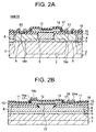
- Fig. 2A is a cross-sectional view along X-X' of Fig. 1
- Fig. 2B is a cross-sectional view along Y-Y' of Fig. 1.
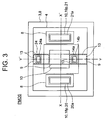
- Fig. 3 is a top view of the conventional high withstand voltage PMOS transistor viewed from an upper side of the substrate
- Fig. 4A is a cross-sectional view along X-X' of Fig. 3
- Fig. 4B is a cross-sectional view along Y-Y' of Fig. 3.
- a broken line represents a part overlapped with a solid line.
- LOD/S LOD offset drain/source
- NMOS transistor shown in Figs. 1, 2A and 2B will be explained in structure as an example.
- a buried layer doped with a p-type impurity (PBL) 3 is formed in a predetermined region of a p-type silicon semiconductor substrate on which an n-type epitaxial layer 5 is formed and a p-well 8 and n-wells 9 are formed in a surface part.
- a gate electrode 14 having side wall protection films 17 at side wall parts is formed via a gate oxide film 12.
- a gate electrode plug 14a is formed on the gate electrode 14, as shown in Fig. 2B.
- an n-type source region 18n and an n-type drain region 19n are formed in the surface of the n-wells 9 separated from each other by the p-well 8. These are connected to a source electrode 20 and a drain electrode 21 respectively.
- a surface of the p-well 8 just below the polycrystalline silicon gate electrode 14 is made an n-channel formation region 22.
- an n-channel region 22 is formed on the surface of the p-well 8.
- parasitic n-channel stopper layers 11 containing a p-type impurity are formed so as to sandwich this n-channel formation region 22 between them. Due to this, the withstand voltage is increased.
- silicon oxide films 15, 16 covering the upper side are formed.
- the PMOS transistor shown in Fig. 3 and Figs. 4A and 4B has a similar structure.
- An n-well 9 is formed on a n-type buried layer 4 formed on the substrate 1.
- a p-type source region 18p and a p-type drain region 19p are formed in the surface of the p-well 8 separated by the n-well 9.
- a surface of the n-well 9 just below the polycrystalline silicon gate electrode 14 is made a p-channel formation region 23.
- parasitic p-channel stopper layers 13 containing an n-type impurity are formed so as to sandwich the p-channel formation region 23 between them. Due to this, the withstand voltage is increased.
- NMOS and PMOS transistors are called LOD/S (LOCOS offset drain/source)-type LDMOS transistors.
- LOD/S LOD offset drain/source
- BV ds junction withstand voltage between source and drain
- the n-type source region 18 and n-type drain region 19 are formed away from the p-well 8 by the LOCOS oxide film 10.
- a depletion layer extends from a junction of the p-well 8 of a low concentration of impurity and the n-well 9 to the n-well 9.
- the withstand voltage is secured by using the extension of the depletion layer to the n-well 9 for easing the electric field.
- the withstand voltage is increased further by employing a RESURF (reduced surface field) technique, that is, easing of the electric field at the surface of the n-well 9 using an extension of a depletion layer at the junction of the p-type silicon semiconductor substrate 1 of a low concentration of impurity and the n-type epitaxial layer 5 of a low concentration of impurity in the surface direction.
- RESURF reduced surface field
- the NMOS transistor shown in Fig. 2 when the NMOS transistor shown in Fig. 2 is in an on state, that is, in the state where the source electrode 20 and drain electrode 21 have any voltage, a positive voltage is supplied on the polycrystalline silicon gate electrode 14, the n-channel 22 is formed as shown in Fig. 2B, and an electric current flows between the source and drain, when the source electrode 20 (or the drain electrode) voltage becomes a high voltage, a high electric field is generated at the junction of the n-channel 22 and the parasitic n-channel stopper layer 11 (parts shown with arrows) and a junction breakdown is sometimes caused.
- An object of the present invention is to provide a semiconductor device comprising a high withstand voltage MOS transistor having an offset drain/offset source structure wherein the high electric field generated between the channel and the parasitic channel stopper in an operating state is eased and changes of the threshold voltage V th , on-resistance R on , or other characteristics are prevented.
- Another object of the present invention is to provide a method of producing the semiconductor device in a high yield.
- a semiconductor device comprising: a substrate; an epitaxial layer formed on the substrate; a source region and a drain region formed in the epitaxial layer and containing a first conductivity type impurity; a source electrode connected to the source region; a drain electrode connected to the drain region; a channel region formed between the source region and drain region; a gate insulating film formed on the channel region; and a gate electrode formed on the gate insulating film, said device comprising at least a second conductivity type channel stopper layer formed in proximity to the channel region in the epitaxial layer except between the source region and/or drain region and the gate electrode, wherein an impurity concentration in a first region of the channel stopper layer near the channel region is lower than an impurity concentration in a second region far from the channel region.
- the semiconductor device further comprises a field insulating film formed on the channel stopper layer.
- the semiconductor device further comprises a field insulating film formed on a surface of the epitaxial layer between the source electrode and/or the drain electrode and the gate electrode.
- the semiconductor device further comprises said field insulating film formed on a surface of the epitaxial layer between the source electrode and/or the drain electrode and the gate electrode.
- the field insulating film is an oxide film.
- a semiconductor device comprising: a first conductivity type substrate; a second conductivity type epitaxial layer formed on the substrate; a first well region and a second well region formed in the epitaxial layer and containing a second conductivity type impurity; a source region formed in the first well region and containing a second conductivity type impurity at a higher concentration than the first well region; a drain region formed in the second well region and containing a second conductivity type impurity at a higher concentration than the second well, region; a source electrode connected to the source region; a drain electrode connected to the drain region; a channel region formed between the source region and the drain region; a gate insulating film formed on the channel region; and a gate electrode formed on the gate insulating film, wherein the channel region is included in at least a first conductivity type third well, said device comprising at least a first conductivity type channel stopper layer formed in proximity to the channel region in the epitaxial layer except between the source region
- the semiconductor device further comprises a field insulating film formed on the channel stopper layer.
- the semiconductor device further comprises a field insulating film formed on a surface of the epitaxial layer between the source electrode and/or the drain electrode and the gate electrode.
- the semiconductor device further comprises the field insulating film formed on a surface of the epitaxial layer between the source electrode and/or the drain electrode and the gate electrode.
- the field insulating film is an oxide film.
- a semiconductor device comprising: a first conductivity type substrate; a second conductivity type buried layer formed in the substrate; a second conductivity type epitaxial layer formed on the substrate; a first well region and a second well region formed in the epitaxial layer and containing a first conductivity type impurity; a source region formed in the first well region and containing a first conductivity type impurity at a higher concentration than the first well region; a drain region formed in the second well region and containing a first conductivity type impurity at a higher concentration than the second well region; a source electrode connected to the source region; a drain electrode connected to the drain region; a channel region formed between the source region and the drain region; a gate insulating film formed on the channel region; and a gate electrode formed on the gate insulating film, wherein the channel region is included in at least a second conductivity type third well, said device comprising at least a second conductivity type channel stopper layer formed in proximity to the
- the semiconductor device further comprises a field insulating film formed on the channel stopper layer.
- the semiconductor device further comprises a field insulating film formed on a surface of the epitaxial layer between the source electrode and/or the drain electrode and the gate electrode.
- the semiconductor device further comprises the field insulating film formed on a surface of the epitaxial layer between the source electrode and/or the drain electrode and the gate electrode.
- the field insulating film is an oxide film.
- a method of producing a semiconductor device for forming a PMOS transistor and an NMOS transistor on a same substrate comprising the steps of: introducing a first conductivity type impurity in the NMOS transistor formation region and introducing a second conductivity type impurity in the PMOS transistor formation region; forming a second conductivity type epitaxial layer on the substrate; forming a first conductivity type first well region in the epitaxial layer of the NMOS transistor formation region and forming first conductivity type second and third well regions in the epitaxial layer of the PMOS transistor formation region; forming second conductivity type fourth and fifth well regions at both edges of the first well region and forming a second conductivity type sixth well region between the second well region and the third well region; forming a first channel stopper layer by introducing a second conductivity type impurity in the epitaxial layer except a direction facing the second well region and/or the third well region and the sixth well region; forming a second channel stopper
- Figure 6 is a top view of a high withstand voltage NMOS transistor of the present embodiment viewed from an upper side of the substrate
- Fig. 7A is a cross-sectional view along X-X' of Fig. 6
- Fig. 7B is a cross-sectional view along Y-Y' of Fig. 6.
- Fig. 8 is a top view of the high withstand voltage PMOS transistor of the present embodiment viewed from an upper side of the substrate
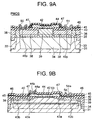
- Fig. 9A is a cross-sectional view along X-X' of Fig. 8
- Fig. 9B is a cross-sectional view along Y-Y' of Fig. 8.
- a broken line represents a part overlapped with a solid line.
- LOD/S LOD offset drain/source
- the NMOS transistor shown in Figs. 7A and 7B has a structure as follows.
- a buried layer doped with a p-type impurity (PBL) 33 is formed in a predetermined region of a p-type silicon semiconductor substrate 31, an n-type epitaxial layer 35 is formed on them, and a p-well 38 and n-well 39 are formed in a surface part.
- the p-well 38 becomes an active region and the n-well 39 becomes an offset source region and offset drain region.
- a gate electrode 44 is formed via a gate oxide film 42.
- an n-type source region 48n and n-type drain region 49n are respectively formed on the surface of the n-well 39 of the offset source region or offset drain region.
- the parasitic n-channel stopper layers 41a, 41b are formed at the junction of the p-well 38 and LOCOS 40 so as to sandwich an n-channel formation region 52 just below the polycrystalline silicon gate electrode 44 between them.
- the parasitic n-channel stopper layers 41a, 41b contain a p-type impurity. The concentration of the p-type impurity becomes smaller at the parasitic n-channel stopper layer 41a approaching the n-channel formation region 52.
- silicon oxide films 45, 46 covering the upper side are formed in the above transistor.
- a backgate electrode 54 is formed via the parasitic n-channel stopper layer 41b.
- a backgate contact 54a part a low resistivity region (backgate plug region) in which a p-type impurity is diffused is formed.
- the PMOS transistor shown in Figs. 9A and 9B has a similar structure.
- Parasitic p-channel stopper layers 43a, 43b are formed just below the LOCOS oxide film 40 at the edge of the polycrystalline silicon gate electrode 44 so as to sandwich the p-channel formation region 53 between them.
- the parasitic p-channel stopper layers 43a, 43b contain an n-type impurity. The concentration of the n-type impurity becomes smaller at the parasitic p-channel stopper layer 43a approaching the p-channel formation region 53.
- the semiconductor device of the present embodiment is a high withstand voltage MOS transistor having a so-called offset drain/offset source structure wherein the parasitic channel stopper layers 41a, 41b or 43a, 43b are formed to have a concentration gradient where their impurity concentrations decrease along with approaching the channel formation regions 52, 53. Due to this, it is possible to ease a high electric field generated between the channel and parasitic channel stopper layer in an operating state.
- the semiconductor device of the present embodiment it is possible to reliably prevent changes of the threshold voltage V th , on-resistance R on , and other characteristics.
- the semiconductor device of the present embodiment realizes a higher withstand voltage by employing the RESURF technique in the same manner as the conventional transistor.
- the semiconductor device of the present embodiment unlike the general LOD-type LDMOS transistors, has a symmetrical structure right and left from the gate, that is, in the direction of the source and the drain, it is possible to increase the withstand voltage not only between a backgate and the drain and between the gate and the drain or other drain sides but also between a backgate and the source and between the gate and source or other source sides.
- the semiconductor device of the present embodiment is free from changes of the threshold voltage V th , on-resistance R on , or other characteristics when forming, for example, an analog switch as shown in Fig. 10. Therefore, it is made possible to transfer an input signal precisely to an output circuit without restriction of the voltage of an input or output signal.
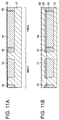
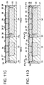
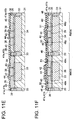
- the second embodiment shows a method of producing a semiconductor device of the present invention. Below, the second embodiment will be explained with reference to Figs. 11A to 11F.
- a silicon oxide film 32 having a thickness of about 60 to 100 nm is formed on a p-type silicon semiconductor substrate 31 by steam-oxidation at about 900 to 1000°C.
- existing photolithography technology and ion-implantation technology are used together with a not shown resist mask for ion implantation of boron of a dose of about 1 X 10 13 to 1 X 10 14 /cm 2 for the purpose of forming a p-type buried layer 33 in an element isolation region and active region of the NMOS transistor.
- the resist mask is removed and existing photolithography technology and ion-implantation technology are used again together with a not shown resist mask for ion implantation of phosphorus of a dose of about 5 X 10 12 to 5 X 10 13 /cm 2 to form an n-type buried layer 34 in the active region of the PMOS transistor.
- the resist mask is removed, then heat treatment is performed at about 1100 to 1200°C to form the p-type buried layer 33 and n-type buried layer 34. As explained above, the structure shown in Fig. 11A is obtained.
- n-type epitaxial layer 35 having a resistivity of about 5 to 10 ⁇ cm.
- the thickness of the n-type epitaxial layer 35 is determined in accordance with the desired withstand voltage, but is generally calculated using as a standard about 10 ⁇ m per 100V.
- a silicon oxide film 36 of 60 to 100 nm is formed on the surface of the n-type epitaxial layer 35 by steam-oxidation at about 900 to 1000°C. As descried above, a structure shown in Fig. 11B is obtained.
- resist mask for ion implantation of boron of about 1 X 10 13 to 1 X 10 14 /cm 2 for the purpose of forming the p-well 38 in the element isolation region, the active region of the NMOS transistor, and the offset drain/offset source formation region of the PMOS transistor.
- resist mask is removed, then existing photolithography technology and ion-implantation technology are again used together with a not shown resist mask for ion implantation of phosphorus of about 5 X 10 12 to 1 X 10 13 /cm 2 for the purpose of forming the n-well 39 in the offset drain/offset source formation region of the NMOS transistor and the active region of the PMOS transistor.
- a silicon nitride (Si 3 N 4 ) film 37 having a thickness of about 80 to 100 nm is formed by low pressure CVD (chemical vapor deposition). Further, the p-well 38 and n-well 39 are formed by heat treatment at about 1100 to 1200°C.
- photolithography technology and ion-implantation technology are used for ion implantation of phosphorus of a dose of about 1 X 10 12 to 1 X 10 13 /cm 2 in a parasitic p-channel stopper layer formation region (region corresponding to the parasitic p-channel stopper layers 43a, 43b of Fig. 8 and Fig. 9B) of the PMOS transistor.
- photolithography technology and ion-implantation technology are used together with a not shown resist mask for ion implantation of phosphorus of a dose of about 1 X 10 13 to 1 X 10 14 /cm 2 in a part of the parasitic p-channel stopper formation region of the PMOS transistor except a part near the p-channel formation region 53 (region corresponding to the parasitic p-channel stopper layer 43b of Fig. 9B).
- a parasitic p-channel stopper layer having a concentration gradient is formed at the same time.
- This parasitic p-channel stopper layer as shown in Fig. 8 and Fig. 9B (see the parasitic p-channel stopper layers 43a, 43b), is formed at the two edges of the channel formation region in the direction of a gate width just below the LOCOS oxide film 40.
- the silicon nitride film 37 is removed with hot phosphoric acid and the silicon oxide film 36 at the surface of the n-type epitaxial layer 35 is removed using a hydrofluoric acid (HF) solution.
- HF hydrofluoric acid
- the gate oxide film 42 of about 100 to 200 nm is formed by steam-oxidation at about 950 to 1000°C (see Fig. 11D).
- photolithography technology and ion-implantation technology are used together with a not shown resist mask for ion implantation of boron of about 5 X 10 12 to 5 X 10 13 /cm 2 in the parasitic n-channel stopper layers 41a, 41b formation region in the element isolation region and NMOS transistor.
- resist mask for ion implantation of boron of about 5 X 10 12 to 5 X 10 13 /cm 2 in the parasitic n-channel stopper layers 41a, 41b formation region in the element isolation region and NMOS transistor.
- photolithography technology and ion-implantation technology are used for ion implantation of boron of about 5 X 10 13 to 5 X 10 14 /cm 2 in the parasitic n-channel stopper layer 41b formation region (region away from the n-channel formation region 52 in the parasitic n-channel stopper layer) in the element isolation region and NMOS transistor.
- the CVD process is used to deposit an n + -type polycrystalline silicon film containing an n-type impurity of about 400 nm.
- photolithography technology and RIE or another existing etching technology are used for etching to leave the n + -polycrystalline silicon only on the gate formation region of the MOS transistor to form the polycrystalline silicon gate electrode 44 (see Fig. 11E).
- photolithography technology and existing etching technology are used to remove the gate oxide film 42 on the source/drain formation region.
- a not shown oxide film of about 10 to 20 nm (corresponding to the silicon oxide film 45 in Fig. 7 and Fig. 9) is formed by steam-oxidation at about 800 to 900°C.
- the resist mask is removed, then photolithography technology and ion-implantation technology are used for ion implantation of As of about 1 X 10 15 to 1 X 10 16 /cm 2 in the source/drain region of the NMOS transistor and a backgate plug region of the PMOS transistor.
- a silicon oxide film 46 having a thickness of about 600 nm is formed by the CVD process and heat treatment is performed at about 850 to 950°C. Due to this, the ion-implanted impurity diffuses and the p-type source region 48p and p-type drain region 49p of the PMOS transistor, the not shown backgate plug region of the NMOS transistor, and the n-type source region 48n and n-type drain region 49n of the NMOS transistor and the not shown backgate plug region of the PMOS transistor are formed.
- the parasitic n-channel stopper layers 41a, 41b of the NMOS transistor are formed.
- the impurity profile of the parasitic n-channel stopper layers 41a, 41b is made less in concentration along with approaching the n-channel formation region 52, so it is made possible to ease a high electric field generated between the n-channel 52 and parasitic n-channel stopper layers 41a, 41b and prevent the changes of the threshold voltage V th , on-resistance R on , or other characteristics.
- photolithography technology and RIE or another existing etching technology are used together with a not shown resist mask to open electrode windows in regions for forming the source electrode 50, drain electrode 51, gate electrode plug 44a, etc. in the silicon oxide film 46.
- a metal electrode containing Al or Ti/TiON/Ti/Al-Si or other barrier metal is vapor deposited in the electrode windows, it is patterned by photolithography technology and RIE technology, then the source electrode 50, drain electrode 51, gate electrode plug 44a, and backgate electrode (not shown) are formed in the NMOS and PMOS.
- the semiconductor device of the present invention by giving the structure a concentration gradient where the concentration of impurity in the parasitic channel stopper layer decreases along with approaching the channel region, it is possible to ease the high electric field generated between the channel and parasitic channel stopper in an operating state and prevent changes of the threshold voltage V th , on-resistance R on , or other characteristics.
Landscapes
- Metal-Oxide And Bipolar Metal-Oxide Semiconductor Integrated Circuits (AREA)
- Insulated Gate Type Field-Effect Transistor (AREA)
- Element Separation (AREA)
Abstract
Description
Claims (19)
- A semiconductor device comprising:a substrate;an epitaxial layer formed on the substrate;a source region and a drain region formed in the epitaxial layer and containing a first conductivity type impurity;a source electrode connected to the source region;a drain electrode connected to the drain region;a channel region formed between the source region and drain region;a gate insulating film formed on the channel region; anda gate electrode formed on the gate insulating film,said device comprising at least a second conductivity type channel stopper layer formed in proximity to the channel region in the epitaxial layer except between the source region and/or drain region and the gate electrode, and
wherein an impurity concentration in a first region of the channel stopper layer near the channel region is lower than an impurity concentration in a second region far from the channel region. - A semiconductor device as set forth in claim 1, further comprising a field insulating film formed on the channel stopper layer.
- A semiconductor device as set forth in claim 1, further comprising a field insulating film formed on a surface of the epitaxial layer between the source electrode and/or the drain electrode and the gate electrode.
- A semiconductor device as set forth in claim 2, further comprising said field insulating film formed on a surface of the epitaxial layer between the source electrode and/or the drain electrode and the gate electrode.
- A semiconductor device as set forth in claim 3, wherein the field insulating film comprises an oxide film.
- A semiconductor device as set forth in claim 4, wherein the field insulating film comprises an oxide film.
- A semiconductor device comprising:a first conductivity type substrate;a second conductivity type epitaxial layer formed on the substrate;a first well region and a second well region formed in the epitaxial layer and containing a second conductivity type impurity;a source region formed in the first well region and containing a second conductivity type impurity at a higher concentration than the first well region;a drain region formed in the second well region and containing a second conductivity type impurity at a higher concentration than the second well region;a source electrode connected to the source region;a drain electrode connected to the drain region;a channel region formed between the source region and the drain region;a gate insulating film formed on the channel region; anda gate electrode formed on the gate insulating film,
wherein the channel region is included in at least a first conductivity type third well,said device comprising at least a first conductivity type channel stopper layer formed in proximity to the channel region in the epitaxial layer except between the source region and/or the drain region and the gate electrode, and
wherein an impurity concentration in a first region of the channel stopper layer near the channel region is lower than an impurity concentration in a second region far from the channel region. - A semiconductor device as set forth in claim 7, further comprising a field insulating film formed on the channel stopper layer.
- A semiconductor device as set forth in claim 7, further comprising a field insulating film formed on a surface of the epitaxial layer between the source electrode and/or the drain electrode and the gate electrode.
- A semiconductor device as set forth in claim 8, further comprising the field insulating film formed on a surface of the epitaxial layer between the source electrode and/or the drain electrode and the gate electrode.
- A semiconductor device as set forth in claim 9, wherein the field insulating film comprises an oxide film.
- A semiconductor device as set forth in claim 10, wherein the field insulating film comprises an oxide film.
- A semiconductor device comprising:a first conductivity type substrate;a second conductivity type buried layer formed in the substrate;a second conductivity type epitaxial layer formed on the substrate;a first well region and a second well region formed in the epitaxial layer and containing a first conductivity type impurity;a source region formed in the first well region and containing a first conductivity type impurity at a higher concentration than the first well region;a drain region formed in the second well region and containing a first conductivity type impurity at a higher concentration than the second well region;a source electrode connected to the source region;a drain electrode connected to the drain region;a channel region formed between the source region and the drain region;a gate insulating film formed on the channel region; anda gate electrode formed on the gate insulating film,
wherein the channel region is included in at least a second conductivity type third well,said device comprising at least a second conductivity type channel stopper layer formed in proximity to the channel region in the epitaxial layer except between the source region and/or the drain region and the gate electrode, and
wherein an impurity concentration in a first region of the channel stopper layer near the channel region is lower than an impurity concentration in a second region far from the channel region. - A semiconductor device as set forth in claim 13, further comprising a field insulating film formed on the channel stopper layer.
- A semiconductor device as set forth in claim 13, further comprising a field insulating film formed on a surface of the epitaxial layer between the source electrode and/or the drain electrode and the gate electrode.
- A semiconductor device as set forth in claim 14, further comprising the field insulating film formed on a surface of the epitaxial layer between the source electrode and/or the drain electrode and the gate electrode.
- A semiconductor device as set forth in claim 15, wherein the field insulating film comprises an oxide film.
- A semiconductor device as set forth in claim 16, wherein the field insulating film comprises an oxide film.
- A method of producing a semiconductor device for forming a PMOS transistor and an NMOS transistor on a same substrate,said method comprising the steps of:introducing a first conductivity type impurity in the NMOS transistor formation region and introducing a second conductivity type impurity in the PMOS transistor formation region;forming a second conductivity type epitaxial layer on the substrate;forming a first conductivity type first well region in the epitaxial layer of the NMOS transistor formation region and forming first conductivity type second and third well regions in the epitaxial layer of the PMOS transistor formation region;forming second conductivity type fourth and fifth well regions at both edges of the first well region and forming a second conductivity type sixth well region between the second well region and the third well region;forming a first channel stopper layer by introducing a second conductivity type impurity in the epitaxial layer except a direction facing the second well region and/or the third well region and the sixth well region;forming a second channel stopper layer by introducing a second conductivity type impurity in the first channel stopper layer of a position farther from the second well region and/or the third well region;forming a LOCOS oxide film between the first well region and the fourth well region, between the first well region and the fifth well region, between the second well region and the sixth well region and between the third well region and the sixth well region;forming a gate insulating film on the first well region and on the sixth well region;after forming the LOCOS oxide film, forming a third channel stopper layer by introducing a first conductivity type impurity in the epitaxial layer except a direction facing the fourth well region and/or the fifth well region and the first well region;forming a fourth channel stopper layer by introducing a first conductivity type impurity in the third channel stopper layer of a position farther from the fourth well region and/or the fifth well region;forming a first conductivity type source region and drain region by introducing further a first conductivity type impurity in the second and third well regions and forming a second conductivity type source region and drain region by introducing further a second conductivity type impurity in the fourth and fifth well regions;forming electrodes connected to the source regions and drain regions respectively; andforming gate electrodes on the gate insulating films respectively.
Applications Claiming Priority (6)
| Application Number | Priority Date | Filing Date | Title |
|---|---|---|---|
| JP26450399 | 1999-09-17 | ||
| JP26450399 | 1999-09-17 | ||
| JP30547799 | 1999-10-27 | ||
| JP30547799 | 1999-10-27 | ||
| JP2000248870A JP4686829B2 (en) | 1999-09-17 | 2000-08-18 | Semiconductor device and manufacturing method of semiconductor device |
| JP2000248870 | 2000-08-18 |
Publications (3)
| Publication Number | Publication Date |
|---|---|
| EP1085574A2 true EP1085574A2 (en) | 2001-03-21 |
| EP1085574A3 EP1085574A3 (en) | 2004-09-15 |
| EP1085574B1 EP1085574B1 (en) | 2007-12-26 |
Family
ID=27335311
Family Applications (1)
| Application Number | Title | Priority Date | Filing Date |
|---|---|---|---|
| EP00120304A Expired - Lifetime EP1085574B1 (en) | 1999-09-17 | 2000-09-15 | Method of producing a semiconductor device |
Country Status (5)
| Country | Link |
|---|---|
| US (1) | US6489657B1 (en) |
| EP (1) | EP1085574B1 (en) |
| JP (1) | JP4686829B2 (en) |
| KR (1) | KR100721464B1 (en) |
| DE (1) | DE60037559T2 (en) |
Cited By (4)
| Publication number | Priority date | Publication date | Assignee | Title |
|---|---|---|---|---|
| WO2007057137A1 (en) * | 2005-11-16 | 2007-05-24 | Austriamicrosystems Ag | High-voltage transistor and component containing the latter |
| DE102011056412A1 (en) * | 2011-12-14 | 2013-06-20 | Austriamicrosystems Ag | High-voltage transistor device and manufacturing method |
| TWI405250B (en) * | 2010-04-13 | 2013-08-11 | Richtek Technology Corp | Method for controlling impurity density distribution in semiconductor device and semiconductor device made thereby |
| CN104425610A (en) * | 2013-09-11 | 2015-03-18 | 株式会社东芝 | Semiconductor device and method of fabricating the same |
Families Citing this family (11)
| Publication number | Priority date | Publication date | Assignee | Title |
|---|---|---|---|---|
| US7235835B2 (en) * | 2002-05-14 | 2007-06-26 | Sony Corporation | Semiconductor device and its manufacturing method, and electronic device |
| JP4603248B2 (en) * | 2003-06-19 | 2010-12-22 | 株式会社Kenzan | Semiconductor element and logic circuit having the same |
| JP2005191202A (en) * | 2003-12-25 | 2005-07-14 | Seiko Epson Corp | Semiconductor device |
| KR100568255B1 (en) * | 2004-01-26 | 2006-04-07 | 삼성전자주식회사 | Bidirectional high voltage switching device and energy recovery circuit including the same |
| JP2006156779A (en) | 2004-11-30 | 2006-06-15 | Seiko Epson Corp | Semiconductor device and manufacturing method thereof |
| DE102005031908B3 (en) * | 2005-07-07 | 2006-10-19 | Infineon Technologies Ag | Semiconductor component e.g. power diode, has channel stop zone whose doping concentration contantly decrease by distance of ten micrometer sectionally in lateral direction towards active component zone |
| KR100836767B1 (en) * | 2007-02-05 | 2008-06-10 | 삼성전자주식회사 | Semiconductor device including MOS transistor for controlling high voltage and forming method thereof |
| KR100840787B1 (en) * | 2007-02-23 | 2008-06-23 | 삼성전자주식회사 | Semiconductor device and manufacturing method of semiconductor device |
| KR101408877B1 (en) | 2007-12-03 | 2014-06-17 | 삼성전자주식회사 | A display driving integrated circuit including a transistor, a high voltage transistor, and the high voltage transistor |
| US9401410B2 (en) * | 2014-11-26 | 2016-07-26 | Texas Instruments Incorporated | Poly sandwich for deep trench fill |
| CN115458603B (en) * | 2022-09-30 | 2025-08-19 | 北京燕东微电子科技有限公司 | Semiconductor device structure and preparation method thereof |
Family Cites Families (13)
| Publication number | Priority date | Publication date | Assignee | Title |
|---|---|---|---|---|
| JPS5368987A (en) * | 1976-12-02 | 1978-06-19 | Fujitsu Ltd | Semiconductor device |
| JPS561571A (en) * | 1979-06-15 | 1981-01-09 | Mitsubishi Electric Corp | Manufacture of mos type semiconductor device |
| JP2687490B2 (en) * | 1988-10-14 | 1997-12-08 | 日本電気株式会社 | Logic integrated circuit |
| JPH02226758A (en) * | 1989-02-28 | 1990-09-10 | Oki Electric Ind Co Ltd | semiconductor equipment |
| JPH04290470A (en) * | 1991-03-19 | 1992-10-15 | Kawasaki Steel Corp | Semiconductor device |
| JP2995931B2 (en) * | 1991-07-29 | 1999-12-27 | 松下電器産業株式会社 | Method for manufacturing semiconductor device |
| JPH0555566A (en) * | 1991-08-28 | 1993-03-05 | Nec Corp | Semiconductor device |
| JPH06216380A (en) * | 1992-10-07 | 1994-08-05 | Matsushita Electric Ind Co Ltd | Semiconductor device and manufacture thereof |
| US5396096A (en) * | 1992-10-07 | 1995-03-07 | Matsushita Electric Industrial Co., Ltd. | Semiconductor device and manufacturing method thereof |
| JPH06232394A (en) * | 1993-02-02 | 1994-08-19 | Rohm Co Ltd | Manufacture of semiconductor device |
| JP2800702B2 (en) * | 1994-10-31 | 1998-09-21 | 日本電気株式会社 | Semiconductor device |
| JP3229837B2 (en) * | 1997-05-30 | 2001-11-19 | 三洋電機株式会社 | Method for manufacturing semiconductor device |
| JP4104701B2 (en) * | 1997-06-26 | 2008-06-18 | 株式会社半導体エネルギー研究所 | Semiconductor device |
-
2000
- 2000-08-18 JP JP2000248870A patent/JP4686829B2/en not_active Expired - Fee Related
- 2000-09-15 EP EP00120304A patent/EP1085574B1/en not_active Expired - Lifetime
- 2000-09-15 DE DE60037559T patent/DE60037559T2/en not_active Expired - Lifetime
- 2000-09-16 KR KR1020000054437A patent/KR100721464B1/en not_active Expired - Fee Related
- 2000-09-18 US US09/664,272 patent/US6489657B1/en not_active Expired - Fee Related
Cited By (9)
| Publication number | Priority date | Publication date | Assignee | Title |
|---|---|---|---|---|
| WO2007057137A1 (en) * | 2005-11-16 | 2007-05-24 | Austriamicrosystems Ag | High-voltage transistor and component containing the latter |
| US9093527B2 (en) | 2005-11-16 | 2015-07-28 | Ams Ag | High-voltage transistor and component containing the latter |
| TWI405250B (en) * | 2010-04-13 | 2013-08-11 | Richtek Technology Corp | Method for controlling impurity density distribution in semiconductor device and semiconductor device made thereby |
| DE102011056412A1 (en) * | 2011-12-14 | 2013-06-20 | Austriamicrosystems Ag | High-voltage transistor device and manufacturing method |
| DE102011056412B4 (en) * | 2011-12-14 | 2013-10-31 | Austriamicrosystems Ag | High-voltage transistor device and manufacturing method |
| CN103988287A (en) * | 2011-12-14 | 2014-08-13 | ams有限公司 | High voltage transistor device and fabrication method |
| US9076676B2 (en) | 2011-12-14 | 2015-07-07 | Ams Ag | High-voltage transistor device and production method |
| CN103988287B (en) * | 2011-12-14 | 2016-05-25 | ams有限公司 | High voltage transistor device and fabrication method |
| CN104425610A (en) * | 2013-09-11 | 2015-03-18 | 株式会社东芝 | Semiconductor device and method of fabricating the same |
Also Published As
| Publication number | Publication date |
|---|---|
| DE60037559T2 (en) | 2008-12-11 |
| JP2001196546A (en) | 2001-07-19 |
| US6489657B1 (en) | 2002-12-03 |
| EP1085574B1 (en) | 2007-12-26 |
| KR20010039893A (en) | 2001-05-15 |
| JP4686829B2 (en) | 2011-05-25 |
| KR100721464B1 (en) | 2007-05-25 |
| EP1085574A3 (en) | 2004-09-15 |
| DE60037559D1 (en) | 2008-02-07 |
Similar Documents
| Publication | Publication Date | Title |
|---|---|---|
| US6855581B2 (en) | Method for fabricating a high-voltage high-power integrated circuit device | |
| US6534837B1 (en) | Semiconductor device | |
| US5585660A (en) | Extended drain resurf lateral DMOS devices | |
| US6869847B2 (en) | Semiconductor device manufacturing method thereof | |
| EP1085574B1 (en) | Method of producing a semiconductor device | |
| US8786013B2 (en) | Trench transistor | |
| US6404009B1 (en) | Semiconductor device and method of producing the same | |
| US20130037883A1 (en) | Ldpmos structure for enhancing breakdown voltage and specific on resistance in bicmos-dmos process | |
| US9390983B1 (en) | Semiconductor device and method for fabricating the same | |
| EP0676799A2 (en) | Extended drain resurf lateral DMOS devices | |
| US7196375B2 (en) | High-voltage MOS transistor | |
| US7166901B2 (en) | Semiconductor device | |
| US10256340B2 (en) | High-voltage semiconductor device and method for manufacturing the same | |
| JP2009004441A (en) | Semiconductor device | |
| US5925916A (en) | Semiconductor processing method of providing electrical isolation between adjacent semiconductor diffusion regions of different field effect transistors and integrated circuitry having adjacent electrically isolated field effect transistors | |
| US10128331B1 (en) | High-voltage semiconductor device and method for manufacturing the same | |
| US20150295027A1 (en) | Semiconductor device and method for fabricating the same | |
| JP4378781B2 (en) | Semiconductor device and manufacturing method thereof | |
| JPH10335484A (en) | Method for manufacturing semiconductor device | |
| US7936023B1 (en) | High voltage diode | |
| JPH11317519A (en) | Semiconductor device and manufacturing method thereof | |
| JPH03119733A (en) | High breakdown-strength semiconductor device | |
| JPH11297996A (en) | Semiconductor device and manufacturing method thereof | |
| EP3261126A1 (en) | High-voltage semiconductor device and method for manufacturing the same | |
| JPH0445568A (en) | Manufacture of mos ic |
Legal Events
| Date | Code | Title | Description |
|---|---|---|---|
| PUAI | Public reference made under article 153(3) epc to a published international application that has entered the european phase |
Free format text: ORIGINAL CODE: 0009012 |
|
| AK | Designated contracting states |
Kind code of ref document: A2 Designated state(s): AT BE CH CY DE DK ES FI FR GB GR IE IT LI LU MC NL PT SE |
|
| AX | Request for extension of the european patent |
Free format text: AL;LT;LV;MK;RO;SI |
|
| PUAL | Search report despatched |
Free format text: ORIGINAL CODE: 0009013 |
|
| AK | Designated contracting states |
Kind code of ref document: A3 Designated state(s): AT BE CH CY DE DK ES FI FR GB GR IE IT LI LU MC NL PT SE |
|
| AX | Request for extension of the european patent |
Extension state: AL LT LV MK RO SI |
|
| 17P | Request for examination filed |
Effective date: 20050225 |
|
| AKX | Designation fees paid |
Designated state(s): DE FR GB |
|
| 17Q | First examination report despatched |
Effective date: 20060123 |
|
| RTI1 | Title (correction) |
Free format text: METHOD OF PRODUCING A SEMICONDUCTOR DEVICE |
|
| GRAP | Despatch of communication of intention to grant a patent |
Free format text: ORIGINAL CODE: EPIDOSNIGR1 |
|
| GRAS | Grant fee paid |
Free format text: ORIGINAL CODE: EPIDOSNIGR3 |
|
| GRAA | (expected) grant |
Free format text: ORIGINAL CODE: 0009210 |
|
| AK | Designated contracting states |
Kind code of ref document: B1 Designated state(s): DE FR GB |
|
| REG | Reference to a national code |
Ref country code: GB Ref legal event code: FG4D |
|
| REF | Corresponds to: |
Ref document number: 60037559 Country of ref document: DE Date of ref document: 20080207 Kind code of ref document: P |
|
| PLBE | No opposition filed within time limit |
Free format text: ORIGINAL CODE: 0009261 |
|
| STAA | Information on the status of an ep patent application or granted ep patent |
Free format text: STATUS: NO OPPOSITION FILED WITHIN TIME LIMIT |
|
| 26N | No opposition filed |
Effective date: 20080929 |
|
| REG | Reference to a national code |
Ref country code: GB Ref legal event code: 746 Effective date: 20091130 |
|
| PGFP | Annual fee paid to national office [announced via postgrant information from national office to epo] |
Ref country code: GB Payment date: 20110920 Year of fee payment: 12 Ref country code: FR Payment date: 20110928 Year of fee payment: 12 Ref country code: DE Payment date: 20110923 Year of fee payment: 12 |
|
| GBPC | Gb: european patent ceased through non-payment of renewal fee |
Effective date: 20120915 |
|
| REG | Reference to a national code |
Ref country code: FR Ref legal event code: ST Effective date: 20130531 |
|
| PG25 | Lapsed in a contracting state [announced via postgrant information from national office to epo] |
Ref country code: DE Free format text: LAPSE BECAUSE OF NON-PAYMENT OF DUE FEES Effective date: 20130403 Ref country code: GB Free format text: LAPSE BECAUSE OF NON-PAYMENT OF DUE FEES Effective date: 20120915 |
|
| PG25 | Lapsed in a contracting state [announced via postgrant information from national office to epo] |
Ref country code: FR Free format text: LAPSE BECAUSE OF NON-PAYMENT OF DUE FEES Effective date: 20121001 |
|
| REG | Reference to a national code |
Ref country code: DE Ref legal event code: R119 Ref document number: 60037559 Country of ref document: DE Effective date: 20130403 |