EP1085573A1 - Method of decreasing the mutual inductance between bond wires in a high frequency amplifying circuit - Google Patents
Method of decreasing the mutual inductance between bond wires in a high frequency amplifying circuit Download PDFInfo
- Publication number
- EP1085573A1 EP1085573A1 EP00304186A EP00304186A EP1085573A1 EP 1085573 A1 EP1085573 A1 EP 1085573A1 EP 00304186 A EP00304186 A EP 00304186A EP 00304186 A EP00304186 A EP 00304186A EP 1085573 A1 EP1085573 A1 EP 1085573A1
- Authority
- EP
- European Patent Office
- Prior art keywords
- semiconductor device
- set forth
- electrical connect
- connect means
- semiconductor chip
- Prior art date
- Legal status (The legal status is an assumption and is not a legal conclusion. Google has not performed a legal analysis and makes no representation as to the accuracy of the status listed.)
- Granted
Links
Images


Classifications
-
- H—ELECTRICITY
- H10—SEMICONDUCTOR DEVICES; ELECTRIC SOLID-STATE DEVICES NOT OTHERWISE PROVIDED FOR
- H10W—GENERIC PACKAGES, INTERCONNECTIONS, CONNECTORS OR OTHER CONSTRUCTIONAL DETAILS OF DEVICES COVERED BY CLASS H10
- H10W44/00—Electrical arrangements for controlling or matching impedance
- H10W44/20—Electrical arrangements for controlling or matching impedance at high-frequency [HF] or radio frequency [RF]
-
- H—ELECTRICITY
- H10—SEMICONDUCTOR DEVICES; ELECTRIC SOLID-STATE DEVICES NOT OTHERWISE PROVIDED FOR
- H10W—GENERIC PACKAGES, INTERCONNECTIONS, CONNECTORS OR OTHER CONSTRUCTIONAL DETAILS OF DEVICES COVERED BY CLASS H10
- H10W72/00—Interconnections or connectors in packages
-
- H—ELECTRICITY
- H10—SEMICONDUCTOR DEVICES; ELECTRIC SOLID-STATE DEVICES NOT OTHERWISE PROVIDED FOR
- H10W—GENERIC PACKAGES, INTERCONNECTIONS, CONNECTORS OR OTHER CONSTRUCTIONAL DETAILS OF DEVICES COVERED BY CLASS H10
- H10W42/00—Arrangements for protection of devices
- H10W42/20—Arrangements for protection of devices protecting against electromagnetic or particle radiation, e.g. light, X-rays, gamma-rays or electrons
- H10W42/261—Arrangements for protection of devices protecting against electromagnetic or particle radiation, e.g. light, X-rays, gamma-rays or electrons characterised by their shapes or dispositions
- H10W42/265—Shielding wires, e.g. constant potential wires
-
- H—ELECTRICITY
- H10—SEMICONDUCTOR DEVICES; ELECTRIC SOLID-STATE DEVICES NOT OTHERWISE PROVIDED FOR
- H10W—GENERIC PACKAGES, INTERCONNECTIONS, CONNECTORS OR OTHER CONSTRUCTIONAL DETAILS OF DEVICES COVERED BY CLASS H10
- H10W44/00—Electrical arrangements for controlling or matching impedance
- H10W44/20—Electrical arrangements for controlling or matching impedance at high-frequency [HF] or radio frequency [RF]
- H10W44/203—Electrical connections
- H10W44/206—Wires
-
- H—ELECTRICITY
- H10—SEMICONDUCTOR DEVICES; ELECTRIC SOLID-STATE DEVICES NOT OTHERWISE PROVIDED FOR
- H10W—GENERIC PACKAGES, INTERCONNECTIONS, CONNECTORS OR OTHER CONSTRUCTIONAL DETAILS OF DEVICES COVERED BY CLASS H10
- H10W70/00—Package substrates; Interposers; Redistribution layers [RDL]
- H10W70/60—Insulating or insulated package substrates; Interposers; Redistribution layers
-
- H—ELECTRICITY
- H10—SEMICONDUCTOR DEVICES; ELECTRIC SOLID-STATE DEVICES NOT OTHERWISE PROVIDED FOR
- H10W—GENERIC PACKAGES, INTERCONNECTIONS, CONNECTORS OR OTHER CONSTRUCTIONAL DETAILS OF DEVICES COVERED BY CLASS H10
- H10W72/00—Interconnections or connectors in packages
- H10W72/071—Connecting or disconnecting
- H10W72/075—Connecting or disconnecting of bond wires
-
- H—ELECTRICITY
- H10—SEMICONDUCTOR DEVICES; ELECTRIC SOLID-STATE DEVICES NOT OTHERWISE PROVIDED FOR
- H10W—GENERIC PACKAGES, INTERCONNECTIONS, CONNECTORS OR OTHER CONSTRUCTIONAL DETAILS OF DEVICES COVERED BY CLASS H10
- H10W72/00—Interconnections or connectors in packages
- H10W72/071—Connecting or disconnecting
- H10W72/075—Connecting or disconnecting of bond wires
- H10W72/07551—Connecting or disconnecting of bond wires characterised by changes in properties of the bond wires during the connecting
- H10W72/07553—Connecting or disconnecting of bond wires characterised by changes in properties of the bond wires during the connecting changes in shapes
-
- H—ELECTRICITY
- H10—SEMICONDUCTOR DEVICES; ELECTRIC SOLID-STATE DEVICES NOT OTHERWISE PROVIDED FOR
- H10W—GENERIC PACKAGES, INTERCONNECTIONS, CONNECTORS OR OTHER CONSTRUCTIONAL DETAILS OF DEVICES COVERED BY CLASS H10
- H10W72/00—Interconnections or connectors in packages
- H10W72/50—Bond wires
- H10W72/531—Shapes of wire connectors
-
- H—ELECTRICITY
- H10—SEMICONDUCTOR DEVICES; ELECTRIC SOLID-STATE DEVICES NOT OTHERWISE PROVIDED FOR
- H10W—GENERIC PACKAGES, INTERCONNECTIONS, CONNECTORS OR OTHER CONSTRUCTIONAL DETAILS OF DEVICES COVERED BY CLASS H10
- H10W72/00—Interconnections or connectors in packages
- H10W72/50—Bond wires
- H10W72/531—Shapes of wire connectors
- H10W72/5366—Shapes of wire connectors the bond wires having kinks
-
- H—ELECTRICITY
- H10—SEMICONDUCTOR DEVICES; ELECTRIC SOLID-STATE DEVICES NOT OTHERWISE PROVIDED FOR
- H10W—GENERIC PACKAGES, INTERCONNECTIONS, CONNECTORS OR OTHER CONSTRUCTIONAL DETAILS OF DEVICES COVERED BY CLASS H10
- H10W72/00—Interconnections or connectors in packages
- H10W72/50—Bond wires
- H10W72/541—Dispositions of bond wires
- H10W72/5445—Dispositions of bond wires being orthogonal to a side surface of the chip, e.g. parallel arrangements
-
- H—ELECTRICITY
- H10—SEMICONDUCTOR DEVICES; ELECTRIC SOLID-STATE DEVICES NOT OTHERWISE PROVIDED FOR
- H10W—GENERIC PACKAGES, INTERCONNECTIONS, CONNECTORS OR OTHER CONSTRUCTIONAL DETAILS OF DEVICES COVERED BY CLASS H10
- H10W72/00—Interconnections or connectors in packages
- H10W72/50—Bond wires
- H10W72/541—Dispositions of bond wires
- H10W72/5449—Dispositions of bond wires not being orthogonal to a side surface of the chip, e.g. fan-out arrangements
-
- H—ELECTRICITY
- H10—SEMICONDUCTOR DEVICES; ELECTRIC SOLID-STATE DEVICES NOT OTHERWISE PROVIDED FOR
- H10W—GENERIC PACKAGES, INTERCONNECTIONS, CONNECTORS OR OTHER CONSTRUCTIONAL DETAILS OF DEVICES COVERED BY CLASS H10
- H10W72/00—Interconnections or connectors in packages
- H10W72/50—Bond wires
- H10W72/551—Materials of bond wires
- H10W72/552—Materials of bond wires comprising metals or metalloids, e.g. silver
-
- H—ELECTRICITY
- H10—SEMICONDUCTOR DEVICES; ELECTRIC SOLID-STATE DEVICES NOT OTHERWISE PROVIDED FOR
- H10W—GENERIC PACKAGES, INTERCONNECTIONS, CONNECTORS OR OTHER CONSTRUCTIONAL DETAILS OF DEVICES COVERED BY CLASS H10
- H10W72/00—Interconnections or connectors in packages
- H10W72/50—Bond wires
- H10W72/551—Materials of bond wires
- H10W72/552—Materials of bond wires comprising metals or metalloids, e.g. silver
- H10W72/5522—Materials of bond wires comprising metals or metalloids, e.g. silver comprising gold [Au]
-
- H—ELECTRICITY
- H10—SEMICONDUCTOR DEVICES; ELECTRIC SOLID-STATE DEVICES NOT OTHERWISE PROVIDED FOR
- H10W—GENERIC PACKAGES, INTERCONNECTIONS, CONNECTORS OR OTHER CONSTRUCTIONAL DETAILS OF DEVICES COVERED BY CLASS H10
- H10W72/00—Interconnections or connectors in packages
- H10W72/50—Bond wires
- H10W72/551—Materials of bond wires
- H10W72/552—Materials of bond wires comprising metals or metalloids, e.g. silver
- H10W72/5524—Materials of bond wires comprising metals or metalloids, e.g. silver comprising aluminium [Al]
-
- H—ELECTRICITY
- H10—SEMICONDUCTOR DEVICES; ELECTRIC SOLID-STATE DEVICES NOT OTHERWISE PROVIDED FOR
- H10W—GENERIC PACKAGES, INTERCONNECTIONS, CONNECTORS OR OTHER CONSTRUCTIONAL DETAILS OF DEVICES COVERED BY CLASS H10
- H10W72/00—Interconnections or connectors in packages
- H10W72/50—Bond wires
- H10W72/551—Materials of bond wires
- H10W72/552—Materials of bond wires comprising metals or metalloids, e.g. silver
- H10W72/5525—Materials of bond wires comprising metals or metalloids, e.g. silver comprising copper [Cu]
-
- H—ELECTRICITY
- H10—SEMICONDUCTOR DEVICES; ELECTRIC SOLID-STATE DEVICES NOT OTHERWISE PROVIDED FOR
- H10W—GENERIC PACKAGES, INTERCONNECTIONS, CONNECTORS OR OTHER CONSTRUCTIONAL DETAILS OF DEVICES COVERED BY CLASS H10
- H10W72/00—Interconnections or connectors in packages
- H10W72/50—Bond wires
- H10W72/59—Bond pads specially adapted therefor
-
- H—ELECTRICITY
- H10—SEMICONDUCTOR DEVICES; ELECTRIC SOLID-STATE DEVICES NOT OTHERWISE PROVIDED FOR
- H10W—GENERIC PACKAGES, INTERCONNECTIONS, CONNECTORS OR OTHER CONSTRUCTIONAL DETAILS OF DEVICES COVERED BY CLASS H10
- H10W72/00—Interconnections or connectors in packages
- H10W72/90—Bond pads, in general
- H10W72/921—Structures or relative sizes of bond pads
- H10W72/926—Multiple bond pads having different sizes
-
- H—ELECTRICITY
- H10—SEMICONDUCTOR DEVICES; ELECTRIC SOLID-STATE DEVICES NOT OTHERWISE PROVIDED FOR
- H10W—GENERIC PACKAGES, INTERCONNECTIONS, CONNECTORS OR OTHER CONSTRUCTIONAL DETAILS OF DEVICES COVERED BY CLASS H10
- H10W72/00—Interconnections or connectors in packages
- H10W72/90—Bond pads, in general
- H10W72/931—Shapes of bond pads
- H10W72/932—Plan-view shape, i.e. in top view
-
- H—ELECTRICITY
- H10—SEMICONDUCTOR DEVICES; ELECTRIC SOLID-STATE DEVICES NOT OTHERWISE PROVIDED FOR
- H10W—GENERIC PACKAGES, INTERCONNECTIONS, CONNECTORS OR OTHER CONSTRUCTIONAL DETAILS OF DEVICES COVERED BY CLASS H10
- H10W72/00—Interconnections or connectors in packages
- H10W72/90—Bond pads, in general
- H10W72/951—Materials of bond pads
-
- H—ELECTRICITY
- H10—SEMICONDUCTOR DEVICES; ELECTRIC SOLID-STATE DEVICES NOT OTHERWISE PROVIDED FOR
- H10W—GENERIC PACKAGES, INTERCONNECTIONS, CONNECTORS OR OTHER CONSTRUCTIONAL DETAILS OF DEVICES COVERED BY CLASS H10
- H10W90/00—Package configurations
- H10W90/701—Package configurations characterised by the relative positions of pads or connectors relative to package parts
- H10W90/751—Package configurations characterised by the relative positions of pads or connectors relative to package parts of bond wires
- H10W90/756—Package configurations characterised by the relative positions of pads or connectors relative to package parts of bond wires between a chip and a stacked lead frame, conducting package substrate or heat sink
Definitions
- the present invention relates to semiconductor devices capable of sufficiently maintaining high frequency properties of high frequency semiconductor chips that operate at high frequencies, especially, in the gigahertz band.
- the stray inductance in wires grows beyond ignorable level.
- the stray inductance in some cases, drastically degrades properties of the integrated circuit, especially, those properties in GHz range.
- bonding wires are used so as to electrically connect the semiconductor chip to the package or circuit substrate.
- the effect of the inductance of the bonding wires is extremely strong: the degradation in the intrinsic performance (especially, high frequency properties) of the circuit in the semiconductor chip is inevitable unless the inductance is reduced sufficiently.
- the effect of the inductance of the bonding wires as signal lines extending from the semiconductor chip can be reduced by matching impedances with an externally connected load circuit; however, such matching is impossible on the inductance of, especially, grounded bonding wires, which end up in behaving as a feedback circuit.
- the inductance reduces the gain introduced by the amplifier circuit in the semiconductor chip, and degrades properties, especially in high frequency band.
- the problem here is how to minimize the inductance when the ground line in, for example, a gallium arsenide (GaAs) semiconductor chip for use at high frequencies is connected to an external ground line or ground surface, such as the package or the circuit substrate, so as to mount the semiconductor chip.
- GaAs gallium arsenide
- a package 80 including a ground electrode 81 for the package 80, as well as input electrodes (lead frame serving as input terminals) 85 for the package 80 and output electrodes 86 for the package 80 disposed in proximity to the ground electrode 81.
- a semiconductor chip 71 disposed on the ground electrode 81 includes thereon a ground terminal 84 for ground use, input terminals 75 for the semiconductor chip 71, and output terminals 76 for the semiconductor chip 71.
- the terminals 75, 76, and 84 of the semiconductor chip 71 are electrically connected respectively to the electrode 85, 86, and 81 of the package 80 by bonding wires 73, 83, and 82.
- Japanese Laid-Open Patent Application No. 2-107001/1990 Japanese Laid-Open Patent Application No. 3-262302/1991 (Tokukaihei 3-262302; published on November 22, 1991), etc. disclose another known technique to shorten the bonding wires whereby the bonding pads are positioned at the same height with the pattern surface of the substrate by arranging the chip so that the chip is connected to the bonding wires at places lower than the rest of the chip; hence, the bonding wires connecting the bonding pads to the pattern surface has a reduced length and a reduced inductance.
- Another technique is known that shortens the wires in their entirety, including the bonding wires, whereby the high-frequency-use semiconductor chip is provided with a small hole through which the ground line inside the chip is connected to the external ground surface on the back of the semiconductor chip.
- Another kind of techniques to shorten the bonding wires is known to reduce the mutual inductance, whereby the bonding wires extending from the ground line inside the semiconductor chip are provided in a maximum number possible and connect to the lead frame or to the slag right beneath the chip, so as to mount, and electrically connect, the high-frequency-use semiconductor chip to the package by wireless bonding.
- the technique is to connect a plurality of bonding wires having an inductance in parallel to each other so as to reduce the total inductance.
- FIG. 6 Shown in Figure 6 as an example is a schematic illustration of a high-frequency-use power amplifier (hereinafter, will be simply referred to as an amplifier circuit) 21 and an amplifier circuit 22 that are integrated into a single chip.
- a high-frequency-use semiconductor chip 23 is constituted by an amplifier circuit 21 and an amplifier circuit 22 ( Figure 6 only shows a bipolar transistor in the output stage).
- the amplifier circuit 21 includes an output bonding pad 27 for the amplifier circuit 21, a ground-use bonding pad 26 for the amplifier circuit 21, and an input bonding pad 34 for the amplifier circuit 21.
- the output bonding pad 27 is connected to, for example, the collector terminal of the high-frequency-use bipolar transistor, whereas the ground-use bonding pad 26 is connected to, for example, the emitter terminal of the high-frequency-use bipolar transistor.
- the amplifier circuit 22 includes an output bonding pad 24 for the amplifier circuit 22, a ground-use bonding pad 25 for the amplifier circuit 22, and an input bonding pad 36 for the amplifier circuit 22.
- the output bonding pad 24 is connected to, for example, the collector terminal of the high-frequency-use bipolar transistor, whereas the ground-use bonding pad 25 is connected to, for example, the emitter terminal of the high-frequency-use bipolar transistor.
- a package 31 as the circuit substrate includes output terminals 32 and 33 for the package 31 to receive outputs from the amplifier circuits 21 and 22 respectively and input terminals 35 and 37 for the package 31 to supply inputs to the amplifier circuits 21 and 22 respectively, as well as a ground electrode 30 which serves as a frame to which the high-frequency-use semiconductor chip 23 is mounted and which also serves as a ground surface.
- bonding wires 50, 41, 38, 39, 28, 29 electrically connect the bonding pads 34, 36, 27, 24, 26, and 25 on the semiconductor chip 23 to the terminals (lead frame) 35, 37, 32, 33, and 30 of the package 31 respectively so as to electrically interconnect the semiconductor chip 23 to the package 31.
- the bonding wires 28 and 29 serve so as to ground the amplifier circuits 21 and 22.
- the bonding wires 28 and 29 are positioned in parallel to each other and perpendicular to a side of the semiconductor chip 23.
- the explanation in the following will focus on the operation of the circuits in the high-frequency-use semiconductor chip 23.
- the two amplifier circuits 21 and 22 are used under such conditions that the amplifier circuit 22 is turned off when the amplifier circuit 21 is in operation, and conversely, the amplifier circuit 21 is turned off when the amplifier circuit 22 is in operation. Consequently, in an ideal state, when the amplifier circuit 21 is activated, the amplifier circuit 22 is isolated, that is, the output terminal 33 of the package 31 does not offer passage to high frequency current, let alone to d.c. current.
- the electromagnetic bonding causes the ground potential (emitter potential) of the bonding pad 25 on the chip containing the amplifier circuit 22 to vary at high frequencies. If the magnitude of the variation grows, the amplifier circuit 22, which should not operate, may be turned on in some cases due to the high frequency (intermittent) variation. When this is the case, a current flow appears at the output terminal 33. To put the problem in different terms, the output signal from the amplifier circuit 21 leaks and appears at the output terminal 33 connected to the amplifier circuit 22. The problem is possibly a cause for a worst scenario: there occurs oscillation, which obstructs normal operation of, and possibly destroy, the high-frequency-use semiconductor chip 23.
- the problem can be solved by forming the amplifier circuits 21 and 22 from individual high frequency semiconductor chips and spacing the amplifier circuits 21 and 22 apart from each other by such an distance that the amplifier circuits 21 and 22 do not interfere with the operation of each other, or by integrating the amplifier circuits 21 and 22 in a single chip but spacing the amplifier circuits 21 and 22 sufficiently apart from each other in that chip.
- the bonding pads are positioned at the same height with the pattern surface of the substrate by arranging the chip so that the chip is connected to the bonding wires at places lower than the rest of the chip; or the high-frequency-use semiconductor chip is provided with a small hole through which the ground line inside the semiconductor chip is connected to the ground surface on the back of the semiconductor chip.
- the present invention has an object to offer a compact, low-cost, and highly reliable high-frequency-use semiconductor device that especially boasts excellent high frequency properties with no increase in chip size and the like and no need to redesign the external terminals and the like of the high-frequency-use semiconductor chip, package, circuit substrate, and the like.
- the semiconductor device in accordance with the present invention in order to solve the foregoing problems, includes:
- the distance between the second contacts on the circuit substrate can be readily increased without a change in the positions of the first contacts at which the electrical connect means are connected to the high-frequency-use semiconductor chip, because the high-frequency-use semiconductor chip is typically smaller in size than the circuit substrate, that is, a package.
- the mutual inductance arising from the electrical connect means can be reduced by providing the electrical connect means so that the distance between the first contacts is smaller than the distance between the second contacts on the circuit substrate. Consequently, with the arrangement, the reduced mutual inductance enables an improvement on reliability, especially, at high frequencies.
- the electrical connect means are preferably for ground use.
- the mutual inductance arising from the electrical connect means is in some cases reducible by an externally connected matching circuit; however, when the electrical connect means are for ground use, it is difficult to reduce the mutual inductance using such a matching circuit.
- the mutual inductance arising from the electrical connect means can be reduced by providing the electrical connect means so that the distance between the first contacts is smaller than the distance between the second contacts on the circuit substrate.
- the reduction of the mutual inductance arising from the ground-use electrical connect means enables an improvement on reliability, especially, at high frequencies.
- the electrical connect means may be electrically conducting bonding wires.
- the bonding wires are ductile, i.e., pliable, the bonding wires as the electrical connect means are readily arranged so that the distance between the first contacts at which the bonding wires are connected to the respective circuit blocks that form an adjacent pair is smaller than the distance between the second contacts at which the bonding wires are connected to the substrate.
- a conductor set to a ground potential is preferably positioned between the electrical connect means that form an adjacent pair distances away from the electrical connect means.
- the conductor set to a ground potential is preferably an electrically conducting wire.
- the ductility, i.e., pliability of the bonding wire facilitates establishment of electrical connection by the wire.
- the conductor set to a ground potential is preferably positioned substantially equal distances away from the electrical connect means that form an adjacent pair. With the arrangement, the provision of the conductor set to a ground potential midway between the electrical connect means that form an adjacent pair ensures the enabling of such specification that further reduces the mutual inductance.
- Figure 1 schematically shows the first embodiment of the semiconductor device in accordance with the present invention.
- the semiconductor device includes a package 11 as a circuit substrate and a substantially rectangular-parallelopiped-shaped high-frequency-use semiconductor chip 3 mounted and electrically connected to the package 11.
- the semiconductor chip 3 has inside thereof, for example, an amplifier circuit 1 for high frequency amplification and an amplifier circuit 2 for high frequency amplification as high frequency circuit blocks.
- an example is taken for the purpose of illustration only, where the semiconductor chip 3 includes the two amplifier circuits 1 and 2; however, the semiconductor chip 3 may include any number of amplifier circuits as long as the amplifier circuits are provided in plurality.
- Figure 1 shows only high-frequency-use bipolar transistors in the output stages, in lieu of the entirety of, the amplifier circuits 1 and 2.
- an output bonding pad 7 for the amplifier circuit 1 and a ground-use bonding pad (first contact) 6 for the amplifier circuit 1 are formed side by side along a longitudinal side of the top surface of the semiconductor chip 3 and stick uncovered out of the top surface.
- the output bonding pad 7 is connected to, for example, the collector terminal of the high-frequency-use bipolar transistor, whereas the ground-use bonding pad 6 is connected to, for example, the emitter terminal of the high-frequency-use bipolar transistor.
- an input bonding pad 14 for the amplifier circuit 1 is formed on the other longitudinal side (the opposing longitudinal side to the foregoing longitudinal side) of the top surface of the semiconductor chip 3 and stick uncovered out of the top surface.
- an output bonding pad 4 for the amplifier circuit 2 a ground-use bonding pad (first contact) 5 for the amplifier circuit 2, and an input bonding pad 16 for the amplifier circuit 2 are formed.
- the output bonding pad 4 is connected to, for example, the collector terminal of the high-frequency-use bipolar transistor, whereas the ground-use bonding pad 5 is connected to, for example, the emitter terminal of the high-frequency-use bipolar transistor.
- the package 11 is provided with input and output terminals 15 and 12 for the amplifier circuit 1 and input and output terminals 17 and 13 for the amplifier circuit 2.
- the package 11 is further provided with a ground electrode 10 on the external surface of the package 11 that serves as a frame constituting a mount and support base for the semiconductor chip 3 and also as a ground surface.
- the ground electrode 10 is specified to have a greater surface area than, preferably twice to thrice as great as, the bottom area of the semiconductor chip 3.
- the input terminals 15 and 17 and the output terminals 12 and 13 are disposed so as to surround the ground electrode 10.
- the semiconductor chip 3 is mounted on the ground electrode 10 so that the peripheral parts of the ground electrode 10 are exposed around the semiconductor chip 3.
- the bonding pads, terminals, and electrodes are all planar and made of a material with good conductance such as copper.
- Bonding wires (electrical connect means) 20, 20', 18, 19, 8, and 9 made of wires of a metal with good conductance, such as gold, silver, copper, or aluminum are provided so as to electrically connect the bonding pads 14, 16, 7, 4, 6, and 5 of the amplifier circuits 1 and 2 in the semiconductor chip 3 to the terminals (lead frame) 15, 17, 12, 13, and 10 of the package 11.
- a metal with excellent ductility is selected to fabricate these bonding wires, so as to allow them to be bent freely with a small force.
- the ground-use bonding wire 8 for the amplifier circuit 1 and the bonding wire 9 for the amplifier circuit 2, which are adjacent to each other, are bonded to the ground electrode 10 so that the distance between the bonding positions (second contacts) on the grounded frame for the package 11, i.e., the ground electrode 10, is large relative to the distance between the semiconductor chip 3 on the bonding pads 6 and 5.
- the bonding wires 8 and 9 are provided so as to extend from the semiconductor chip 3 to the ground electrode 10 of the package 11 in such a manner that the distance between the bonding wires 8 and 9 increases monotonously at a fixed rate toward the distal ends of the bonding wires 8 and 9.
- the bonding wires 8 and 9 arranged in this fashion are preferred, because the foregoing distance can be efficiently increased by the symmetric positioning of the bonding wires 8 and 9 with respect to the surface that is perpendicular to a longitudinal side of the semiconductor chip 3 and that contains the midpoint between the bonding pads 6 and 5 on the semiconductor chip 3.
- the bonding wires 8 and 9 may be arranged in alternative fashions. If one of the bonding wires 8 and 9 can extend only perpendicular to a side of the semiconductor chip 3, it is sufficient to arrange the other bonding wire so that the distance between the bonding wires 8 and 9 increases toward the ground electrode 10, albeit asymmetric. If both the bonding wires 8 and 9 extend diagonally at right or smaller angles to a side of the semiconductor chip 3, it is sufficient to arrange the bonding wires 8 and 9 so that the distance between them increases toward the ground electrode 10, albeit asymmetric.
- the optimum value of the ratio is satisfactorily specified according to the operating frequency, operating current, required characteristics, overall layout of the package 11, and wireless bonding rules, and preferably in the range of 1.2 to 3, more preferably in the range of 1.3 to 2.5, and most preferably in the range of 1.4 to 2.2.
- the other bonding wires 18, 19, 20, and 20' may be arranged in parallel to the mutually adjacent ground-use bonding wires 8 and 9 or the signal-use bonding wires 18, 19, 20, 20', or may be bonded so as to extend from the bonding pads 14, 16, 7, 4 on the semiconductor chip 3 toward the terminals 15, 17, 12 and 13 respectively in such a manner that the distance between these bonding wires increases toward the distal ends thereof.
- the circuits in the high-frequency-use the semiconductor chip 3 operate in the same manner as in the conventional technology explained earlier.
- the two amplifier circuits 1 and 2 are used under such conditions that the amplifier circuit 2 is turned off when the amplifier circuit 1 is in operation, and conversely, the amplifier circuit 1 is turned off when the amplifier circuit 2 is in operation.
- Figure 2(a) is a side view showing the shape and other nature of the bonding wires used in the simulation.
- the bonding wires are shaped like a mound, as an example, by the use of a wireless bonding device.
- the bonding wire 9 is constituted by three continuous portions: i.e., a rising portion 9a, a horizontal portion 9b, and a falling portion 9c.
- the rising portion 9a extends diagonally upward so as to be increasingly separated from the ground electrode 10.
- the horizontal portion 9b starts where the rising portion 9a ends, and extends horizontally, i.e., parallel to the surface of the ground electrode 10.
- the falling portion 9c starts where the horizontal portion 9b ends, extends diagonally downward, i.e. so as to be increasingly closer to the ground electrode 10.
- the three portions when combined, extend the whole length from the 200 ⁇ m-high bonding pad 5 on the top surface of the semiconductor chip 3 to the bonding position of the ground electrode 10.
- the rising portion 9a rises, for example, 180 ⁇ m above the bonding pad 5 located on an edge of the semiconductor chip and is, when measured perpendicular to a side of the semiconductor chip 3, 25 ⁇ m long. It is also specified that the horizontal portion 9b is 75 ⁇ m long and that the falling portion 9c is 600 ⁇ m long and 380 ⁇ m (180 ⁇ m + 200 ⁇ m) high.
- Figure 2(a) and Figure 2(b) are simplified views showing characterizing parts of the semiconductor device of Figure 1 in accordance with the present invention.
- the bonding pads 5 and 6, fabricated from, for example, 90 ⁇ m by 90 ⁇ m ideal metal were disposed on the surface of the semiconductor chip 3 containing a GaAs semiconductor substrate, interconnected with the frame-shaped ground electrode 10 by the ground-use bonding wires 8 and 9, so as to provide grounding to the amplifier circuits 1 and 2.
- the bonding wires 8 and 9 were made from an elongated rectangular ideal metal having a width of 25 ⁇ m and no thickness.
- the frequency was set to 2GHz.
- Bonding coefficients were determined from simulation involving two conventional ground-use bonding wires and two ground-use bonding wires in accordance with the present invention for comparative purposes.
- the ground-use bonding wires 28 and 29 were positioned perpendicular to the high-frequency-use semiconductor chip 23 and parallel to each other.
- the distance between the bonding positions on the ground electrode 10 was specified to be greater than the distance between the bonding pads 5 and 6 on the semiconductor chip 3.
- the "x"-signs and solid line represent conventional samples where the distance, W, between the bonding pads 26 and 25 was varied from 100 ⁇ m to 400 ⁇ m.
- the bonding coefficient K varied from 0.245 to 0.03. It is understood that in the conventional samples, mutual inductance could be reduced in half by expanding the distance W between the bonding pads 26 and 25 from 140 ⁇ m to 250 ⁇ m.
- the bonding wires of the shape shown in Figure 2(a) and Figure 2(b) were employed, and the distance between the bonding pads 6 and 5 on the semiconductor chip 3 was specified to 140 ⁇ m.
- the bonding wires 8 and 9 were disposed so as to extend 100 ⁇ m perpendicular to the semiconductor chip 3 and then extend further with an increasing distance between the bonding wires 8 and 9, before being bonded onto the ground electrode 10 at points 600 ⁇ m away from the bonding pads 6 and 5 when measured along a straight line.
- the distance between the bonding wires 8 and 9 on the ground electrode 10 was specified to 250 ⁇ m.
- the bonding coefficient K between the two adjacent ground-use bonding wires 8 and 9 was determined to be about 0.09 as shown by a solid triangle " ⁇ " in Figure 4. From this, it is understood that isolation, i.e., a reduced mutual inductance arising from the bonding wires 8 and 9, which was equivalent to that in mounting by the conventional technique such that the distance between the parallel bonding wires 28 and 29 was increased to about 220 ⁇ m, was successfully achieved without expanding the distance between the bonding pads 6 and 5 on the semiconductor chip 3.
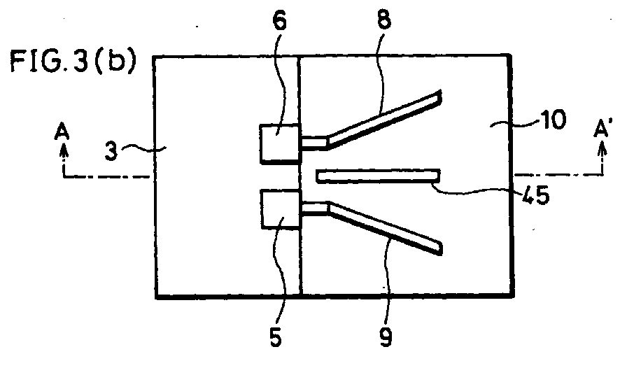
- a dummy wire (dummy conductor) 45 connected to the ground electrode 10 (set to a ground potential) but to none of the bonding pads 4, 5, 6, 7, 14, 16 on the semiconductor chip 3 is mounted by bonding midway between the bonding wires 8 and 9 in the empty space between the bonding wires 8 and 9 of the first embodiment (see Figure 2 (a) and Figure 2 (b)).
- the dummy wire 45 is positioned distances away from the two ground-use bonding wires 8 and 9, more preferably, substantially midway between the bonding wires 8 and 9 (substantially equal distances away from the bonding wires 8 and 9), in other words, on a plane which is perpendicular to a longitudinal side of the semiconductor chip 3 and which contains the midpoint between the bonding pads 6 and 5 on the semiconductor chip 3.
- the dummy wire 45 is specified to have the same height with the ground-use bonding wires 8 and 9 and the same length with the bonding wires 8 and 9 extending from the semiconductor chip 3 to the ground electrode 10, the length being measured along a straight line.
- the two ground-use bonding wires 8 and 9 are provided so as to extend to the ground electrode 10 in such a manner that the distance between the bonding wires 8 and 9 steadily increases starting at their proximal ends (the ends attached to the semiconductor chip 3) to their distal ends (the ends attached to the ground electrode 10). This results in expansion of the empty space between the bonding wires 8 and 9, which facilitates the mounting of the dummy wire 45 to the ground electrode 10 in that empty space.
- the solid square " ⁇ " in Figure 4 represents effects of the provision of the dummy wire 45 as determined by simulation.
- the two ground-use bonding wires 8 and 9 are mounted according to the same specifications as in the first embodiment.
- the provision of the dummy wire 45 caused the bonding coefficient K representative of the mutual inductance arising from the bonding wires 8 and 9 to equal about 0.075. It is understood that isolation, i.e., a reduced mutual inductance of the bonding wires 8 and 9, which was equivalent to that in mounting by the conventional technique such that the distance between the parallel bonding wires 28 and 29 was increased to about 270 ⁇ m, was successfully achieved.
- the present invention is still applicable to circuitry in which both of the bonding wires are used to carry signals (including bonding wires used for any purpose including power supply, except for the provision of grounding), and also to circuitry in which one of the bonding wires is used for grounding and the other for carrying signals.
- the present invention is most effectively applied to the semiconductor chip 3 containing the amplifier circuit 1 producing a gain in high frequency range (higher than 1MHz, more preferably from 100MHz to 100GHz).
- the present invention is applicable in mounting of any kind of high-frequency-use semiconductor elements that requires a reduced level of interference.
- the present invention produces similar effects when applied in mounting of a high-frequency-use semiconductor chip to the package in an upside-down position after formation of bumps at the terminals of the high-frequency-use semiconductor chip, by extending the internal package wiring and substrate wiring to the exterior to the high-frequency-use semiconductor chip through its terminals and expanding the distances between wires.
- the present invention successfully realizes highly reliable operation of the semiconductor chip 3, especially, at high frequencies through reduction in the mutual inductance arising from, for example, the bonding wires 8 and 9 as the electrical connect means that form an adjacent pair with no increase in size of the semiconductor chip 3, by, when electrically connecting the high-frequency-use the semiconductor chip 3 to the package 11 or the substrate, specifying the distance between the terminals on the semiconductor chip 3 as being smaller than the distance between the terminals of the package 11 or the substrate.
- the present invention successfully achieves a further reduction in the mutual inductance by providing a ground-potential-connected dummy wire 45 substantially midway between, for example, the bonding wires 8 and 9 as the electrical connect means that form an adjacent pair.
- the bonding wires 8 and 9, as well as the dummy wire 45 can be installed using an existent bonding device, and thereby no extra cost is needed.
- the present invention requires no customized processing in contrast to the foregoing example where a concave portion is formed in the die bond section to mechanically reduce the wire length, thereby effecting the same advantages at lower cost by far.
- the present invention can obviously further reduce the inductance
- the power amplifiers as the amplifier circuits 1 and 2 need to be designed so as to possess a reduced output impedance, in other words, produce an increased current amplitude, from the transistor in the output stage. Since the effects of the mutual inductance grow in direct proportion to the magnitude of current variation, when the current amplitude needs to be specified to a great value as in the power amplifiers above, the present invention can achieve especially large effects.
- the present invention is capable of reducing the inductance, and especially so in such applications that high frequency electric waves (for example, waves in a 1GHz to 10GHz range) are employed where the inductance arising from the ground electrode 10 as a ground line becomes a major factor to degrade the overall performance of the amplifier circuits 1 and 2. Therefore, the present invention is very useful in the utilization of high frequency electric waves in, for example, cellular phones.
- high frequency electric waves for example, waves in a 1GHz to 10GHz range
Landscapes
- Wire Bonding (AREA)
- Semiconductor Integrated Circuits (AREA)
- Lead Frames For Integrated Circuits (AREA)
- Bipolar Transistors (AREA)
Abstract
wherein the electrical connect means are provided such that the distance between bonding pads serving as first contacts at which the bonding wires are electrically connected to the respective amplifier circuits that form an adjacent pair is smaller than the distance between second contacts at which the bonding wires are electrically connected to the package. With the arrangement, a compact, low-cost, and highly reliable high-frequency-use semiconductor device can be offered with no increase in chip size and the like and no need to redesign the external terminals and the like of the high-frequency-use semiconductor chip, package, circuit substrate, and the like.
Description
- The present invention relates to semiconductor devices capable of sufficiently maintaining high frequency properties of high frequency semiconductor chips that operate at high frequencies, especially, in the gigahertz band.
- In recent years, demand has been growing for integrated circuits capable of operating at microwaves and milliwaves, in response to wide-spread use of mobile telecommunications systems such as PHSs (Personal Handy Phone System) and PDCs (Personal Digital Cellular Phone). Thus, Si and GaAs transistors have been developed for use in such integrated circuits, which in turn led to on-going development of highly integrated MMICs (Monolithic Microwave Integrated Circuits), such as power amplifiers, mixers, and low noise amplifiers, incorporating those transistors.
- In an integrated circuit operating in a high frequency band, the stray inductance in wires grows beyond ignorable level. The stray inductance, in some cases, drastically degrades properties of the integrated circuit, especially, those properties in GHz range.
- For example, to package or mount a semiconductor chip including a high frequency circuit on a circuit substrate, bonding wires are used so as to electrically connect the semiconductor chip to the package or circuit substrate. In that situation, the effect of the inductance of the bonding wires is extremely strong: the degradation in the intrinsic performance (especially, high frequency properties) of the circuit in the semiconductor chip is inevitable unless the inductance is reduced sufficiently.
- Specifically, the effect of the inductance of the bonding wires as signal lines extending from the semiconductor chip can be reduced by matching impedances with an externally connected load circuit; however, such matching is impossible on the inductance of, especially, grounded bonding wires, which end up in behaving as a feedback circuit. Thus, the inductance reduces the gain introduced by the amplifier circuit in the semiconductor chip, and degrades properties, especially in high frequency band.
- So, the problem here is how to minimize the inductance when the ground line in, for example, a gallium arsenide (GaAs) semiconductor chip for use at high frequencies is connected to an external ground line or ground surface, such as the package or the circuit substrate, so as to mount the semiconductor chip.
- Conventionally, there are two kinds of techniques used popularly to reduce the inductance. One of them is to shorten the bonding wires to a minimal possible extent so as to reduce their inductance.
- A typical example of techniques of this kind is described for use in mounting in "LDMOS Devices Provide High Power for Digital PCS", Applied Microwave & Wireless, pp. 84-88, October (1988), by Cindy Blair.
- In the course of mounting, a semiconductor chip is placed on a ground electrode, and bonding wires are positioned in parallel to each other and perpendicular to the sides of a high-frequency-use semiconductor chip, to minimize the length of, especially, the grounded bonding wires. Shown in Figure 5 is a schematic illustration of this mounting technique.
- To further explain the mounting, as shown in Figure 5, there is provided a
package 80 including aground electrode 81 for thepackage 80, as well as input electrodes (lead frame serving as input terminals) 85 for thepackage 80 andoutput electrodes 86 for thepackage 80 disposed in proximity to theground electrode 81. - A
semiconductor chip 71 disposed on theground electrode 81 includes thereon aground terminal 84 for ground use,input terminals 75 for thesemiconductor chip 71, andoutput terminals 76 for thesemiconductor chip 71. - The
terminals semiconductor chip 71 are electrically connected respectively to theelectrode package 80 bybonding wires - Japanese Laid-Open Patent Application No. 2-107001/1990 (Tokukaihei 2-107001; published on April 19, 1990), Japanese Laid-Open Patent Application No. 3-262302/1991 (Tokukaihei 3-262302; published on November 22, 1991), etc. disclose another known technique to shorten the bonding wires whereby the bonding pads are positioned at the same height with the pattern surface of the substrate by arranging the chip so that the chip is connected to the bonding wires at places lower than the rest of the chip; hence, the bonding wires connecting the bonding pads to the pattern surface has a reduced length and a reduced inductance.
- Another technique is known that shortens the wires in their entirety, including the bonding wires, whereby the high-frequency-use semiconductor chip is provided with a small hole through which the ground line inside the chip is connected to the external ground surface on the back of the semiconductor chip.
- Apart from the foregoing kind of techniques to shorten the bonding wires, another kind of techniques is known to reduce the mutual inductance, whereby the bonding wires extending from the ground line inside the semiconductor chip are provided in a maximum number possible and connect to the lead frame or to the slag right beneath the chip, so as to mount, and electrically connect, the high-frequency-use semiconductor chip to the package by wireless bonding. The technique is to connect a plurality of bonding wires having an inductance in parallel to each other so as to reduce the total inductance.
- Incidentally, development in high integration of high-frequency-use semiconductor chips and increasing demand for smaller and cheaper circuits have resulted in a growing trend of a single high-frequency-use semiconductor chip incorporating circuits that have been conventionally offered as separately packaged high-frequency-use semiconductor chips. Shown in Figure 6 as an example is a schematic illustration of a high-frequency-use power amplifier (hereinafter, will be simply referred to as an amplifier circuit) 21 and an
amplifier circuit 22 that are integrated into a single chip. As shown in Figure 6, a high-frequency-use semiconductor chip 23 is constituted by anamplifier circuit 21 and an amplifier circuit 22 (Figure 6 only shows a bipolar transistor in the output stage). - The
amplifier circuit 21 includes anoutput bonding pad 27 for theamplifier circuit 21, a ground-use bonding pad 26 for theamplifier circuit 21, and aninput bonding pad 34 for theamplifier circuit 21. Theoutput bonding pad 27 is connected to, for example, the collector terminal of the high-frequency-use bipolar transistor, whereas the ground-use bonding pad 26 is connected to, for example, the emitter terminal of the high-frequency-use bipolar transistor. - Similarly, the
amplifier circuit 22 includes anoutput bonding pad 24 for theamplifier circuit 22, a ground-use bonding pad 25 for theamplifier circuit 22, and aninput bonding pad 36 for theamplifier circuit 22. Theoutput bonding pad 24 is connected to, for example, the collector terminal of the high-frequency-use bipolar transistor, whereas the ground-use bonding pad 25 is connected to, for example, the emitter terminal of the high-frequency-use bipolar transistor. - Further, a
package 31 as the circuit substrate includesoutput terminals 32 and 33 for thepackage 31 to receive outputs from theamplifier circuits input terminals package 31 to supply inputs to theamplifier circuits ground electrode 30 which serves as a frame to which the high-frequency-use semiconductor chip 23 is mounted and which also serves as a ground surface. - Then,
bonding wires bonding pads semiconductor chip 23 to the terminals (lead frame) 35, 37, 32, 33, and 30 of thepackage 31 respectively so as to electrically interconnect thesemiconductor chip 23 to thepackage 31. Among those bonding wires, thebonding wires amplifier circuits bonding wires semiconductor chip 23. - The explanation in the following will focus on the operation of the circuits in the high-frequency-
use semiconductor chip 23. The twoamplifier circuits amplifier circuit 22 is turned off when theamplifier circuit 21 is in operation, and conversely, theamplifier circuit 21 is turned off when theamplifier circuit 22 is in operation. Consequently, in an ideal state, when theamplifier circuit 21 is activated, theamplifier circuit 22 is isolated, that is, the output terminal 33 of thepackage 31 does not offer passage to high frequency current, let alone to d.c. current. - However, in the foregoing conventional example, especially in a situation such that the
bonding wires bonding pads bonding wires - The electromagnetic bonding causes the ground potential (emitter potential) of the
bonding pad 25 on the chip containing theamplifier circuit 22 to vary at high frequencies. If the magnitude of the variation grows, theamplifier circuit 22, which should not operate, may be turned on in some cases due to the high frequency (intermittent) variation. When this is the case, a current flow appears at the output terminal 33. To put the problem in different terms, the output signal from theamplifier circuit 21 leaks and appears at the output terminal 33 connected to theamplifier circuit 22. The problem is possibly a cause for a worst scenario: there occurs oscillation, which obstructs normal operation of, and possibly destroy, the high-frequency-use semiconductor chip 23. - The problem can be solved by forming the
amplifier circuits amplifier circuits amplifier circuits amplifier circuits amplifier circuits - Such solutions, however, has drawbacks: an increased number of steps required in mounting and an increased overall size of the chip. This in turn constitutes an obstacle in development of cheaper and smaller chips.
- As mentioned above, conventional techniques exist to further shorten the bonding wires: the bonding pads are positioned at the same height with the pattern surface of the substrate by arranging the chip so that the chip is connected to the bonding wires at places lower than the rest of the chip; or the high-frequency-use semiconductor chip is provided with a small hole through which the ground line inside the semiconductor chip is connected to the ground surface on the back of the semiconductor chip. However, these techniques result in complicated manufacturing processes and higher cost.
- As mentioned above, a further conventional technique exist whereby a plurality of bonding wires are connected in parallel to each other. However, such connection results in increased numbers of bonding pads on the chip and terminals (lead frame) of the package, which hinders further development for smaller chips and packages.
- The present invention has an object to offer a compact, low-cost, and highly reliable high-frequency-use semiconductor device that especially boasts excellent high frequency properties with no increase in chip size and the like and no need to redesign the external terminals and the like of the high-frequency-use semiconductor chip, package, circuit substrate, and the like.
- The semiconductor device in accordance with the present invention, in order to solve the foregoing problems, includes:
- a high-frequency-use semiconductor chip including high frequency circuit blocks;
- a circuit substrate on which the semiconductor chip is mounted; and
- electrical connect means each provided for
electrically connecting one of the high frequency circuit
blocks in the semiconductor chip to the circuit
substrate, and
is characterized in that the electrical connect means are provided such that a distance between first contacts at which the electrical connect means are connected to the respective high frequency circuit blocks is smaller than a distance between second contacts at which the electrical connect means are connected to the circuit substrate. -
- With the arrangement, the distance between the second contacts on the circuit substrate can be readily increased without a change in the positions of the first contacts at which the electrical connect means are connected to the high-frequency-use semiconductor chip, because the high-frequency-use semiconductor chip is typically smaller in size than the circuit substrate, that is, a package.
- Hence, with the arrangement, the mutual inductance arising from the electrical connect means can be reduced by providing the electrical connect means so that the distance between the first contacts is smaller than the distance between the second contacts on the circuit substrate. Consequently, with the arrangement, the reduced mutual inductance enables an improvement on reliability, especially, at high frequencies.
- In the semiconductor device, the electrical connect means are preferably for ground use. Generally, the mutual inductance arising from the electrical connect means is in some cases reducible by an externally connected matching circuit; however, when the electrical connect means are for ground use, it is difficult to reduce the mutual inductance using such a matching circuit.
- By contrast, with the arrangement, even if each of the electrical connect means is for ground use, the mutual inductance arising from the electrical connect means can be reduced by providing the electrical connect means so that the distance between the first contacts is smaller than the distance between the second contacts on the circuit substrate.
- As a result, with the arrangement, the reduction of the mutual inductance arising from the ground-use electrical connect means enables an improvement on reliability, especially, at high frequencies.
- In the semiconductor device, the electrical connect means may be electrically conducting bonding wires. With the arrangement, since the bonding wires are ductile, i.e., pliable, the bonding wires as the electrical connect means are readily arranged so that the distance between the first contacts at which the bonding wires are connected to the respective circuit blocks that form an adjacent pair is smaller than the distance between the second contacts at which the bonding wires are connected to the substrate.
- In the semiconductor device, a conductor set to a ground potential is preferably positioned between the electrical connect means that form an adjacent pair distances away from the electrical connect means. With the arrangement, the provision of the conductor set to a ground potential enables such specification that further reduces the mutual inductance.
- In the semiconductor device, the conductor set to a ground potential is preferably an electrically conducting wire. With the arrangement, the ductility, i.e., pliability of the bonding wire facilitates establishment of electrical connection by the wire.
- In the semiconductor device, the conductor set to a ground potential is preferably positioned substantially equal distances away from the electrical connect means that form an adjacent pair. With the arrangement, the provision of the conductor set to a ground potential midway between the electrical connect means that form an adjacent pair ensures the enabling of such specification that further reduces the mutual inductance.
- The present invention will become more fully understood from the detailed description given hereinbelow and the accompanying drawings which are given by way of illustration only, are not in any way intended to limit the scope of the claims of the present invention.
-
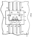
- Figure 1 is a plan view schematically showing a semiconductor device of a first embodiment in accordance with the present invention.
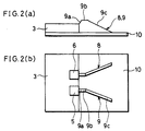
- Figure 2(a) and Figure 2(b) are explanatory views showing a major part of the semiconductor device, Figure 2(a) being a schematic cross-sectional view, Figure 2(b) being a schematic plan view.
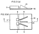
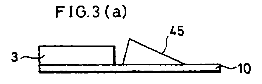
- Figure 3(a) and Figure 3(b) are explanatory views schematically showing a semiconductor device of a second embodiment in accordance with the present invention, Figure 3 (a) being a schematic cross-sectional view, Figure 3 (b) being a schematic plan view.
- Figure 4 is a graph showing the above-mentioned semiconductor devices having a successfully reduced inductance compared with conventional semiconductor devices.
- Figure 5 is a plan view schematically showing a conventional semiconductor device.
- Figure 6 is a plan view schematically showing another conventional semiconductor device.
- Figure 7(a) and Figure 7(b) are explanatory views showing a major part of a conventional semiconductor device for the purpose of comparison with those semiconductor devices in accordance with the present invention, Figure 7(a) being a schematic cross-sectional view, Figure 7(b) being a schematic plan view.
-
- Referring to Figures 1, 2(a), 2(b), 4, 7(a), and 7(b), the following will discuss a first embodiment in accordance with the present invention.
- Figure 1 schematically shows the first embodiment of the semiconductor device in accordance with the present invention. As shown in Figure 1, the semiconductor device includes a
package 11 as a circuit substrate and a substantially rectangular-parallelopiped-shaped high-frequency-use semiconductor chip 3 mounted and electrically connected to thepackage 11. - The
semiconductor chip 3 has inside thereof, for example, anamplifier circuit 1 for high frequency amplification and anamplifier circuit 2 for high frequency amplification as high frequency circuit blocks. Here, an example is taken for the purpose of illustration only, where thesemiconductor chip 3 includes the twoamplifier circuits semiconductor chip 3 may include any number of amplifier circuits as long as the amplifier circuits are provided in plurality. Note that Figure 1 shows only high-frequency-use bipolar transistors in the output stages, in lieu of the entirety of, theamplifier circuits - In the
semiconductor chip 3, anoutput bonding pad 7 for theamplifier circuit 1 and a ground-use bonding pad (first contact) 6 for theamplifier circuit 1 are formed side by side along a longitudinal side of the top surface of thesemiconductor chip 3 and stick uncovered out of the top surface. Theoutput bonding pad 7 is connected to, for example, the collector terminal of the high-frequency-use bipolar transistor, whereas the ground-use bonding pad 6 is connected to, for example, the emitter terminal of the high-frequency-use bipolar transistor. - Further, an
input bonding pad 14 for theamplifier circuit 1 is formed on the other longitudinal side (the opposing longitudinal side to the foregoing longitudinal side) of the top surface of thesemiconductor chip 3 and stick uncovered out of the top surface. - In the
semiconductor chip 3, similarly to theamplifier circuit 1, an output bonding pad 4 for theamplifier circuit 2, a ground-use bonding pad (first contact) 5 for theamplifier circuit 2, and aninput bonding pad 16 for theamplifier circuit 2 are formed. The output bonding pad 4 is connected to, for example, the collector terminal of the high-frequency-use bipolar transistor, whereas the ground-use bonding pad 5 is connected to, for example, the emitter terminal of the high-frequency-use bipolar transistor. - The
package 11 is provided with input andoutput terminals amplifier circuit 1 and input andoutput terminals amplifier circuit 2. Thepackage 11 is further provided with aground electrode 10 on the external surface of thepackage 11 that serves as a frame constituting a mount and support base for thesemiconductor chip 3 and also as a ground surface. - Accordingly, the
ground electrode 10 is specified to have a greater surface area than, preferably twice to thrice as great as, the bottom area of thesemiconductor chip 3. Theinput terminals output terminals ground electrode 10. Thesemiconductor chip 3 is mounted on theground electrode 10 so that the peripheral parts of theground electrode 10 are exposed around thesemiconductor chip 3. The bonding pads, terminals, and electrodes are all planar and made of a material with good conductance such as copper. - Bonding wires (electrical connect means) 20, 20', 18, 19, 8, and 9 made of wires of a metal with good conductance, such as gold, silver, copper, or aluminum are provided so as to electrically connect the
bonding pads amplifier circuits semiconductor chip 3 to the terminals (lead frame) 15, 17, 12, 13, and 10 of thepackage 11. A metal with excellent ductility is selected to fabricate these bonding wires, so as to allow them to be bent freely with a small force. - Especially, the ground-
use bonding wire 8 for theamplifier circuit 1 and thebonding wire 9 for theamplifier circuit 2, which are adjacent to each other, are bonded to theground electrode 10 so that the distance between the bonding positions (second contacts) on the grounded frame for thepackage 11, i.e., theground electrode 10, is large relative to the distance between thesemiconductor chip 3 on thebonding pads - To explain the connection in more detail, the
bonding wires semiconductor chip 3 to theground electrode 10 of thepackage 11 in such a manner that the distance between thebonding wires bonding wires - The
bonding wires bonding wires semiconductor chip 3 and that contains the midpoint between thebonding pads semiconductor chip 3. - However, if this arrangement is not available, the
bonding wires bonding wires semiconductor chip 3, it is sufficient to arrange the other bonding wire so that the distance between thebonding wires ground electrode 10, albeit asymmetric. If both thebonding wires semiconductor chip 3, it is sufficient to arrange thebonding wires ground electrode 10, albeit asymmetric. - In these situations, the greater the ratio of the distance on the
ground electrode 10 to that on thesemiconductor chip 3, the smaller the bonding coefficient, but the longer thebonding wires package 11, and wireless bonding rules, and preferably in the range of 1.2 to 3, more preferably in the range of 1.3 to 2.5, and most preferably in the range of 1.4 to 2.2. - The
other bonding wires use bonding wires use bonding wires bonding pads semiconductor chip 3 toward theterminals - The circuits in the high-frequency-use the
semiconductor chip 3 operate in the same manner as in the conventional technology explained earlier. The twoamplifier circuits amplifier circuit 2 is turned off when theamplifier circuit 1 is in operation, and conversely, theamplifier circuit 1 is turned off when theamplifier circuit 2 is in operation. - Simulation was executed for the mutual inductance of the adjacent ground-
use bonding wires - Figure 2(a) is a side view showing the shape and other nature of the bonding wires used in the simulation. In Figure 2 (a), the bonding wires are shaped like a mound, as an example, by the use of a wireless bonding device.
- To further explain the mound-like-shape by taking one of the two bonding wires as an example, the
bonding wire 9 is constituted by three continuous portions: i.e., a risingportion 9a, ahorizontal portion 9b, and a fallingportion 9c. The risingportion 9a extends diagonally upward so as to be increasingly separated from theground electrode 10. Thehorizontal portion 9b starts where the risingportion 9a ends, and extends horizontally, i.e., parallel to the surface of theground electrode 10. The fallingportion 9c starts where thehorizontal portion 9b ends, extends diagonally downward, i.e. so as to be increasingly closer to theground electrode 10. The three portions, when combined, extend the whole length from the 200µm-high bonding pad 5 on the top surface of thesemiconductor chip 3 to the bonding position of theground electrode 10. - It is specified that the rising
portion 9a rises, for example, 180µm above thebonding pad 5 located on an edge of the semiconductor chip and is, when measured perpendicular to a side of thesemiconductor chip 3, 25µm long. It is also specified that thehorizontal portion 9b is 75µm long and that the fallingportion 9c is 600µm long and 380µm (180µm + 200µm) high. - Figure 2(a) and Figure 2(b) are simplified views showing characterizing parts of the semiconductor device of Figure 1 in accordance with the present invention. As shown in Figure 2 (a) and Figure 2 (b), the
bonding pads semiconductor chip 3 containing a GaAs semiconductor substrate, interconnected with the frame-shapedground electrode 10 by the ground-use bonding wires amplifier circuits bonding wires - Bonding coefficients were determined from simulation involving two conventional ground-use bonding wires and two ground-use bonding wires in accordance with the present invention for comparative purposes. In conventional samples, as shown in Figure 7(a) and Figure 7(b), the ground-
use bonding wires use semiconductor chip 23 and parallel to each other. In samples in accordance with the present invention, the distance between the bonding positions on theground electrode 10 was specified to be greater than the distance between thebonding pads semiconductor chip 3. - In conventional samples, the distance between the
bonding pads use bonding wires bonding pads bonding wires bonding pads - In Figure 4, the "x"-signs and solid line represent conventional samples where the distance, W, between the
bonding pads bonding pads - However, according to the conventional technique, since the distance between the
bonding pads semiconductor chip 23 of a larger size to accommodate the pads, which will adds to the cost. - Now, in samples in accordance with the present invention, the bonding wires of the shape shown in Figure 2(a) and Figure 2(b) were employed, and the distance between the
bonding pads semiconductor chip 3 was specified to 140µm. Specifically, thebonding wires semiconductor chip 3 and then extend further with an increasing distance between thebonding wires ground electrode 10 at points 600µm away from thebonding pads bonding wires ground electrode 10 was specified to 250µm. - The bonding coefficient K between the two adjacent ground-
use bonding wires bonding wires parallel bonding wires bonding pads semiconductor chip 3. - Referring to Figures 3(a), 3(b), and 4, the following will discuss a second embodiment of the semiconductor device in accordance with the present invention. Here, the arrangement of the circuits in the high-frequency-use the
semiconductor chip 3 and the specifications of thebonding pads - In the present, second embodiment, a dummy wire (dummy conductor) 45 connected to the ground electrode 10 (set to a ground potential) but to none of the
bonding pads semiconductor chip 3 is mounted by bonding midway between thebonding wires bonding wires - The
dummy wire 45 is positioned distances away from the two ground-use bonding wires bonding wires 8 and 9 (substantially equal distances away from thebonding wires 8 and 9), in other words, on a plane which is perpendicular to a longitudinal side of thesemiconductor chip 3 and which contains the midpoint between thebonding pads semiconductor chip 3. - Further, in the present form of simulation, the
dummy wire 45 is specified to have the same height with the ground-use bonding wires bonding wires semiconductor chip 3 to theground electrode 10, the length being measured along a straight line. - In the present, second embodiment, the two ground-
use bonding wires ground electrode 10 in such a manner that the distance between thebonding wires bonding wires dummy wire 45 to theground electrode 10 in that empty space. - The solid square "▪" in Figure 4 represents effects of the provision of the
dummy wire 45 as determined by simulation. The two ground-use bonding wires - In the second embodiment, as shown in Figure 4, the provision of the
dummy wire 45 caused the bonding coefficient K representative of the mutual inductance arising from thebonding wires bonding wires parallel bonding wires - In the second embodiment so far, the description focused on the provision of the
dummy wire 45 as an example. Alternatively, other conductors may be provided in the same manner to replace thedummy wire 45, and still produce the same effects as those described above. It will be obvious that the present invention is by no means limited by the foregoing first and second embodiments, and may vary in many ways. Such variations are not to be regarded as a departure from the spirit and scope of the invention, and all such modifications as would be obvious to one skilled in the art intended to be included within the scope of the following claims. - Apart from those cases where the
bonding wires amplifier circuits - It will be obvious that apart from the mounting of bonding wires extending from the bonding pads on the
semiconductor chip 3 to the terminals (lead frame) of a package, the same technique is applicable to wireless bonding to terminals on the circuit substrate with similar effects. - The present invention is most effectively applied to the
semiconductor chip 3 containing theamplifier circuit 1 producing a gain in high frequency range (higher than 1MHz, more preferably from 100MHz to 100GHz). However, the present invention is applicable in mounting of any kind of high-frequency-use semiconductor elements that requires a reduced level of interference. - The description so far focused on an application, as an example, where the high-frequency-
use semiconductor chip 3 was mounted with its top surface upward and electrically connected to the terminals (lead frame) of thepackage 11 or the circuit substrate by bonding wires. Alternatively, the present invention produces similar effects when applied in mounting of a high-frequency-use semiconductor chip to the package in an upside-down position after formation of bumps at the terminals of the high-frequency-use semiconductor chip, by extending the internal package wiring and substrate wiring to the exterior to the high-frequency-use semiconductor chip through its terminals and expanding the distances between wires. - As discussed in detail in the foregoing, the present invention successfully realizes highly reliable operation of the
semiconductor chip 3, especially, at high frequencies through reduction in the mutual inductance arising from, for example, thebonding wires semiconductor chip 3, by, when electrically connecting the high-frequency-use thesemiconductor chip 3 to thepackage 11 or the substrate, specifying the distance between the terminals on thesemiconductor chip 3 as being smaller than the distance between the terminals of thepackage 11 or the substrate. - Besides, the present invention successfully achieves a further reduction in the mutual inductance by providing a ground-potential-connected
dummy wire 45 substantially midway between, for example, thebonding wires - In addition, the
bonding wires dummy wire 45, can be installed using an existent bonding device, and thereby no extra cost is needed. Further, the present invention requires no customized processing in contrast to the foregoing example where a concave portion is formed in the die bond section to mechanically reduce the wire length, thereby effecting the same advantages at lower cost by far. However, when employed in combination with this method of mechanically reducing the wire length, the present invention can obviously further reduce the inductance - Incidentally, to obtain a great output power despite the recently prevalent, reduced drive voltage, the power amplifiers as the
amplifier circuits - As discussed earlier, the present invention is capable of reducing the inductance, and especially so in such applications that high frequency electric waves (for example, waves in a 1GHz to 10GHz range) are employed where the inductance arising from the
ground electrode 10 as a ground line becomes a major factor to degrade the overall performance of theamplifier circuits - The invention being thus described, it will be obvious that the same may be varied in many ways. Such variations are not to be regarded as a departure from the spirit and scope of the invention, and all such modifications as would be obvious to one skilled in the art intended to be included within the scope of the following claims.
Claims (19)
- A semiconductor device, comprising:a high-frequency-use semiconductor chip including high frequency circuit blocks;a circuit substrate on which the semiconductor chip is mounted; andelectrical connect means each provided for electrically connecting one of the high frequency circuit blocks in the semiconductor chip to the circuit substrate,
wherein the electrical connect means are provided such that a distance between first contacts at which the electrical connect means are connected to the respective high frequency circuit blocks is smaller than a distance between second contacts at which the electrical connect means are connected to the circuit substrate. - The semiconductor device as set forth in claim 1, whereinthe electrical connect means are used to provide grounding.
- The semiconductor device as set forth in claim 1, whereinthe electrical connect means are electrically conducting bonding wires.
- The semiconductor device as set forth in claim 1, whereinthe distance between the second contacts is 1.2 to 3 times that between the first contacts.
- The semiconductor device as set forth in claim 1, whereinthe high frequency circuit blocks are mutually adjacent.
- The semiconductor device as set forth in claim 1, whereinthe electrical connect means are provided such that the distance between the electrical connect means increases starting at the first contacts toward the second contacts.
- The semiconductor device as set forth in claim 1, whereinthe electrical connect means are provided such that the distance between the electrical connect means monotonously increases starting at the first contacts toward the second contacts.
- The semiconductor device as set forth in claim 1, whereinthe electrical connect means are provided such that the distance between the electrical connect means increases starting at the first contacts toward the second contacts at a fixed rate.
- The semiconductor device as set forth in claim 1, whereinthe circuit substrate includes a ground electrode serving as the second contacts for the electrical connect means.
- The semiconductor device as set forth in claim 9, whereinthe semiconductor chip is mounted on the ground electrode.
- The semiconductor device as set forth in claim 10, whereinthe ground electrode has a surface area greater than a bottom area of the semiconductor chip
- The semiconductor device as set forth in claim 1, whereinan adjacent pair of the electrical connect means are provided so as to be symmetric with respect to a virtual plane crossing the circuit substrate where the second contacts are disposed.
- The semiconductor device as set forth in claim 12, whereinthe virtual symmetric plane crosses the circuit substrate at substantially right angles.
- The semiconductor device as set forth in claim 1, whereina dummy conductor set to a ground potential is positioned between the electrical connect means distances away from the electrical connect means.
- The semiconductor device as set forth in claim 14, whereinthe dummy conductor is an electrically conducting wire.
- The semiconductor device as set forth in claim 14, whereinthe dummy conductor is positioned substantially equal distances away from the electrical connect means that form an adjacent pair.
- The semiconductor device as set forth in claim 14, whereinthe dummy conductor is positioned midway between the electrical connect means that form an adjacent pair.
- The semiconductor device as set forth in claim 1, whereinat least one of the high frequency circuit blocks includes an amplifier circuit having a gain at 1MHz or higher frequencies.
- A semiconductor device comprising high-frequency circuit blocks mounted on a substrate and at least one pair of divergent connecting means connecting the circuit blocks to points on the substrate.
Applications Claiming Priority (2)
| Application Number | Priority Date | Filing Date | Title |
|---|---|---|---|
| JP26589299A JP3539549B2 (en) | 1999-09-20 | 1999-09-20 | Semiconductor device |
| JP26589299 | 1999-09-20 |
Publications (2)
| Publication Number | Publication Date |
|---|---|
| EP1085573A1 true EP1085573A1 (en) | 2001-03-21 |
| EP1085573B1 EP1085573B1 (en) | 2007-12-05 |
Family
ID=17423559
Family Applications (1)
| Application Number | Title | Priority Date | Filing Date |
|---|---|---|---|
| EP00304186A Expired - Lifetime EP1085573B1 (en) | 1999-09-20 | 2000-05-17 | Method of decreasing the mutual inductance between bond wires in a high frequency amplifying circuit |
Country Status (6)
| Country | Link |
|---|---|
| US (1) | US6414387B1 (en) |
| EP (1) | EP1085573B1 (en) |
| JP (1) | JP3539549B2 (en) |
| KR (1) | KR100372845B1 (en) |
| DE (1) | DE60037297T2 (en) |
| TW (1) | TW454283B (en) |
Cited By (2)
| Publication number | Priority date | Publication date | Assignee | Title |
|---|---|---|---|---|
| WO2008074446A1 (en) * | 2006-12-16 | 2008-06-26 | Atmel Germany Gmbh | Semiconductor component |
| WO2008121142A1 (en) * | 2007-04-02 | 2008-10-09 | Kulicke And Soffa Industries, Inc. | Method of forming bends in a wire loop |
Families Citing this family (15)
| Publication number | Priority date | Publication date | Assignee | Title |
|---|---|---|---|---|
| JP4290314B2 (en) * | 2000-04-26 | 2009-07-01 | Necエレクトロニクス株式会社 | High-frequency circuit, module mounted with the same, and communication device |
| JP4843129B2 (en) * | 2000-06-30 | 2011-12-21 | ルネサスエレクトロニクス株式会社 | Semiconductor device and manufacturing method thereof |
| JP4426166B2 (en) * | 2002-11-01 | 2010-03-03 | ユー・エム・シー・ジャパン株式会社 | Semiconductor device design method, semiconductor device design program, and semiconductor device |
| DE10319900A1 (en) * | 2003-04-29 | 2004-11-25 | Infineon Technologies Ag | Optoelectronic transmission and / or reception arrangement |
| JP2005032871A (en) * | 2003-07-09 | 2005-02-03 | Renesas Technology Corp | Semiconductor device |
| JP2005252099A (en) * | 2004-03-05 | 2005-09-15 | Sharp Corp | High frequency semiconductor devices |
| US20050248028A1 (en) * | 2004-05-05 | 2005-11-10 | Cheng-Yen Huang | Chip-packaging with bonding options connected to a package substrate |
| US20060145312A1 (en) * | 2005-01-05 | 2006-07-06 | Kai Liu | Dual flat non-leaded semiconductor package |
| US7898092B2 (en) * | 2007-11-21 | 2011-03-01 | Alpha & Omega Semiconductor, | Stacked-die package for battery power management |
| US7884454B2 (en) * | 2005-01-05 | 2011-02-08 | Alpha & Omega Semiconductor, Ltd | Use of discrete conductive layer in semiconductor device to re-route bonding wires for semiconductor device package |
| US9257375B2 (en) | 2009-07-31 | 2016-02-09 | Alpha and Omega Semiconductor Inc. | Multi-die semiconductor package |
| US8164199B2 (en) * | 2009-07-31 | 2012-04-24 | Alpha and Omega Semiconductor Incorporation | Multi-die package |
| US10014266B2 (en) * | 2016-07-26 | 2018-07-03 | Raytheon Company | Monolithic microwave integrated circuit (MMIC) and method for forming such MMIC having rapid thermal annealing compensation elements |
| DE102016224631B4 (en) * | 2016-12-09 | 2020-06-04 | Fraunhofer-Gesellschaft zur Förderung der angewandten Forschung e.V. | Electrically conductive connection between at least two electrical components on a carrier equipped with electronic and / or electrical components, which is formed with a bonding wire |
| JP7426702B2 (en) * | 2020-02-13 | 2024-02-02 | ザインエレクトロニクス株式会社 | semiconductor equipment |
Citations (1)
| Publication number | Priority date | Publication date | Assignee | Title |
|---|---|---|---|---|
| US5606196A (en) * | 1995-10-14 | 1997-02-25 | Samsung Electronics Co., Ltd. | High-frequency, high-density semiconductor chip package with screening bonding wires |
Family Cites Families (7)
| Publication number | Priority date | Publication date | Assignee | Title |
|---|---|---|---|---|
| JPS60189958A (en) * | 1984-03-09 | 1985-09-27 | Nec Kansai Ltd | semiconductor equipment |
| US4686492A (en) * | 1985-03-04 | 1987-08-11 | Tektronix, Inc. | Impedance match connection using multiple layers of bond wires |
| JPH02107001A (en) | 1988-10-17 | 1990-04-19 | Matsushita Electric Ind Co Ltd | High frequency circuit equipment |
| JPH03262302A (en) | 1990-03-13 | 1991-11-22 | Toshiba Corp | High frequency circuit board |
| JPH06275771A (en) | 1993-03-23 | 1994-09-30 | Hitachi Ltd | Semiconductor device and semiconductor chip incorporated in the semiconductor device |
| JP3262302B2 (en) | 1993-04-09 | 2002-03-04 | 大日本印刷株式会社 | Phase shift photomask, blank for phase shift photomask, and method of manufacturing the same |
| WO1996041377A1 (en) * | 1995-06-07 | 1996-12-19 | The Panda Project | High performance semiconductor die carrier |
-
1999
- 1999-09-20 JP JP26589299A patent/JP3539549B2/en not_active Expired - Lifetime
-
2000
- 2000-05-15 US US09/571,659 patent/US6414387B1/en not_active Expired - Lifetime
- 2000-05-17 DE DE60037297T patent/DE60037297T2/en not_active Expired - Lifetime
- 2000-05-17 EP EP00304186A patent/EP1085573B1/en not_active Expired - Lifetime
- 2000-05-18 TW TW089109587A patent/TW454283B/en not_active IP Right Cessation
- 2000-05-23 KR KR10-2000-0027783A patent/KR100372845B1/en not_active Expired - Fee Related
Patent Citations (1)
| Publication number | Priority date | Publication date | Assignee | Title |
|---|---|---|---|---|
| US5606196A (en) * | 1995-10-14 | 1997-02-25 | Samsung Electronics Co., Ltd. | High-frequency, high-density semiconductor chip package with screening bonding wires |
Non-Patent Citations (3)
| Title |
|---|
| BENTON B: "RIBBON BONDING", ADVANCED PACKAGING,US,IHS PUBLISHING GROUP, vol. 8, no. 3, March 1999 (1999-03-01), pages 24 - 26, XP000803305, ISSN: 1065-0555 * |
| LEE H -Y: "WIDEBAND CHARACTERIZATION OF MUTUAL COUPLING BETWEEN HIGH DENSITY BONDING WIRES", IEEE MICROWAVE AND GUIDED WAVE LETTERS,US,IEEE INC, NEW YORK, vol. 4, no. 8, 1 August 1994 (1994-08-01), pages 265 - 267, XP000458790, ISSN: 1051-8207 * |
| YUN S -K ET AL: "PARASITIC IMPEDANCE ANALYSIS OF DOUBLE BONDING WIRES FOR HIGH-FREQUENCY INTEGRATED CIRCUIT PACKAGING", IEEE MICROWAVE AND GUIDED WAVE LETTERS,US,IEEE INC, NEW YORK, vol. 5, no. 9, 1 September 1995 (1995-09-01), pages 296 - 298, XP000522577, ISSN: 1051-8207 * |
Cited By (2)
| Publication number | Priority date | Publication date | Assignee | Title |
|---|---|---|---|---|
| WO2008074446A1 (en) * | 2006-12-16 | 2008-06-26 | Atmel Germany Gmbh | Semiconductor component |
| WO2008121142A1 (en) * | 2007-04-02 | 2008-10-09 | Kulicke And Soffa Industries, Inc. | Method of forming bends in a wire loop |
Also Published As
| Publication number | Publication date |
|---|---|
| US6414387B1 (en) | 2002-07-02 |
| EP1085573B1 (en) | 2007-12-05 |
| KR100372845B1 (en) | 2003-02-19 |
| JP2001094009A (en) | 2001-04-06 |
| KR20010049390A (en) | 2001-06-15 |
| JP3539549B2 (en) | 2004-07-07 |
| DE60037297T2 (en) | 2008-10-23 |
| DE60037297D1 (en) | 2008-01-17 |
| TW454283B (en) | 2001-09-11 |
Similar Documents
| Publication | Publication Date | Title |
|---|---|---|
| EP1085573B1 (en) | Method of decreasing the mutual inductance between bond wires in a high frequency amplifying circuit | |
| US7952434B2 (en) | Semiconductor device | |
| CN100380651C (en) | Semiconductor device and electronic apparatus | |
| JP3483132B2 (en) | High frequency semiconductor device | |
| US8035203B2 (en) | Radio frequency over-molded leadframe package | |
| CN114362698A (en) | Power Amplifier Module | |
| US5852391A (en) | Microwave/millimeter-wave functional module package | |
| CN110556365A (en) | Matching circuits for integrated circuit wafers | |
| CN101789421B (en) | Semiconductor device | |
| JPH11238851A (en) | Integrated circuit device and communication device using the same | |
| CN1797760A (en) | Connection arrangement structure for micro lead frame plastic packages | |
| US5530285A (en) | Low-impedance surface-mount device | |
| US6049126A (en) | Semiconductor package and amplifier employing the same | |
| JP2006528854A (en) | Small impedance conversion circuit | |
| NL2027022B1 (en) | Electronic package and device comprising the same | |
| CN100536123C (en) | Semiconductor device and electronic device | |
| JP3913937B2 (en) | Semiconductor device | |
| JP3667136B2 (en) | RF power amplifier module | |
| JP2001284490A (en) | High frequency grounding structure | |
| JP2839023B2 (en) | Semiconductor package and amplifier using the same | |
| JPH09102519A (en) | Semiconductor integrated circuit device | |
| JPH11243161A (en) | Integrated circuit module |
Legal Events
| Date | Code | Title | Description |
|---|---|---|---|
| PUAI | Public reference made under article 153(3) epc to a published international application that has entered the european phase |
Free format text: ORIGINAL CODE: 0009012 |
|
| AK | Designated contracting states |
Kind code of ref document: A1 Designated state(s): DE FR GB |
|
| AX | Request for extension of the european patent |
Free format text: AL;LT;LV;MK;RO;SI |
|
| 17P | Request for examination filed |
Effective date: 20010606 |
|
| AKX | Designation fees paid |
Free format text: DE FR GB |
|
| 17Q | First examination report despatched |
Effective date: 20040813 |
|
| GRAP | Despatch of communication of intention to grant a patent |
Free format text: ORIGINAL CODE: EPIDOSNIGR1 |
|
| GRAS | Grant fee paid |
Free format text: ORIGINAL CODE: EPIDOSNIGR3 |
|
| GRAA | (expected) grant |
Free format text: ORIGINAL CODE: 0009210 |
|
| AK | Designated contracting states |
Kind code of ref document: B1 Designated state(s): DE FR GB |
|
| REG | Reference to a national code |
Ref country code: GB Ref legal event code: FG4D |
|
| REF | Corresponds to: |
Ref document number: 60037297 Country of ref document: DE Date of ref document: 20080117 Kind code of ref document: P |
|
| ET | Fr: translation filed | ||
| PLBE | No opposition filed within time limit |
Free format text: ORIGINAL CODE: 0009261 |
|
| STAA | Information on the status of an ep patent application or granted ep patent |
Free format text: STATUS: NO OPPOSITION FILED WITHIN TIME LIMIT |
|
| 26N | No opposition filed |
Effective date: 20080908 |
|
| PGFP | Annual fee paid to national office [announced via postgrant information from national office to epo] |
Ref country code: DE Payment date: 20120510 Year of fee payment: 13 |
|
| PGFP | Annual fee paid to national office [announced via postgrant information from national office to epo] |
Ref country code: GB Payment date: 20120516 Year of fee payment: 13 Ref country code: FR Payment date: 20120608 Year of fee payment: 13 |
|
| GBPC | Gb: european patent ceased through non-payment of renewal fee |
Effective date: 20130517 |
|
| PG25 | Lapsed in a contracting state [announced via postgrant information from national office to epo] |
Ref country code: DE Free format text: LAPSE BECAUSE OF NON-PAYMENT OF DUE FEES Effective date: 20131203 |
|
| REG | Reference to a national code |
Ref country code: FR Ref legal event code: ST Effective date: 20140131 |
|
| REG | Reference to a national code |
Ref country code: DE Ref legal event code: R119 Ref document number: 60037297 Country of ref document: DE Effective date: 20131203 |
|
| PG25 | Lapsed in a contracting state [announced via postgrant information from national office to epo] |
Ref country code: GB Free format text: LAPSE BECAUSE OF NON-PAYMENT OF DUE FEES Effective date: 20130517 |
|
| PG25 | Lapsed in a contracting state [announced via postgrant information from national office to epo] |
Ref country code: FR Free format text: LAPSE BECAUSE OF NON-PAYMENT OF DUE FEES Effective date: 20130531 |