EP1085535A1 - Planartransformator - Google Patents
Planartransformator Download PDFInfo
- Publication number
- EP1085535A1 EP1085535A1 EP00116058A EP00116058A EP1085535A1 EP 1085535 A1 EP1085535 A1 EP 1085535A1 EP 00116058 A EP00116058 A EP 00116058A EP 00116058 A EP00116058 A EP 00116058A EP 1085535 A1 EP1085535 A1 EP 1085535A1
- Authority
- EP
- European Patent Office
- Prior art keywords
- carrier
- planar transformer
- transformer according
- windings
- current windings
- Prior art date
- Legal status (The legal status is an assumption and is not a legal conclusion. Google has not performed a legal analysis and makes no representation as to the accuracy of the status listed.)
- Granted
Links
- 238000004804 winding Methods 0.000 claims abstract description 37
- 238000009413 insulation Methods 0.000 claims abstract description 5
- RYGMFSIKBFXOCR-UHFFFAOYSA-N Copper Chemical compound [Cu] RYGMFSIKBFXOCR-UHFFFAOYSA-N 0.000 claims description 5
- 229910052802 copper Inorganic materials 0.000 claims description 5
- 239000010949 copper Substances 0.000 claims description 5
- 239000004020 conductor Substances 0.000 claims description 3
- 239000011248 coating agent Substances 0.000 claims description 2
- 238000000576 coating method Methods 0.000 claims description 2
- 238000010276 construction Methods 0.000 description 2
- 238000005516 engineering process Methods 0.000 description 2
- 238000001746 injection moulding Methods 0.000 description 2
- 238000005253 cladding Methods 0.000 description 1
- 239000003973 paint Substances 0.000 description 1
Images

Classifications
-
- H—ELECTRICITY
- H01—ELECTRIC ELEMENTS
- H01F—MAGNETS; INDUCTANCES; TRANSFORMERS; SELECTION OF MATERIALS FOR THEIR MAGNETIC PROPERTIES
- H01F27/00—Details of transformers or inductances, in general
- H01F27/28—Coils; Windings; Conductive connections
- H01F27/2847—Sheets; Strips
- H01F27/2852—Construction of conductive connections, of leads
-
- H—ELECTRICITY
- H01—ELECTRIC ELEMENTS
- H01F—MAGNETS; INDUCTANCES; TRANSFORMERS; SELECTION OF MATERIALS FOR THEIR MAGNETIC PROPERTIES
- H01F27/00—Details of transformers or inductances, in general
- H01F27/02—Casings
- H01F27/027—Casings specially adapted for combination of signal type inductors or transformers with electronic circuits, e.g. mounting on printed circuit boards
-
- H—ELECTRICITY
- H01—ELECTRIC ELEMENTS
- H01F—MAGNETS; INDUCTANCES; TRANSFORMERS; SELECTION OF MATERIALS FOR THEIR MAGNETIC PROPERTIES
- H01F27/00—Details of transformers or inductances, in general
- H01F27/28—Coils; Windings; Conductive connections
- H01F27/29—Terminals; Tapping arrangements for signal inductances
- H01F27/292—Surface mounted devices
Definitions
- the invention relates to a planar transformer with high current windings, a multilayer structure, the layers of flat electrically conductive windings and arranged in between Insulations are formed, one by the turns surrounding magnetic core and a carrier for the multilayer construction.
- the object of the invention is to provide a planar transformer to create the type mentioned, in which the electrical Contacting the high-current windings is simplified.
- the carrier can preferably be made of Plastic, for example by plastic injection molding, be made.
- the carrier and those integrated in it High current windings have the shape of a rectangular and square frame with a central hole through which a Part of the magnetic core protrudes.
- the one from the flat electric conductive windings and interposed insulation formed multilayer structure (multilayer) can on the top and / or be arranged on the underside of the carrier.
- the high-current winding connections led out of the carrier can be designed in the form of connection tabs and are preferably led out laterally on one side of the frame. Can on the opposite side of the frame further connections in the form of connecting pins or for SMD technology for contacting the multi-layer structure (multilayer) existing turns can be provided.
- the carrier thus forms a connection carrier for all turns of the Planar transformers.
- the high current windings can be molded from an electrical conductive material, e.g. Copper. In the high-current windings are preferably stamped parts or bracket formed. A high current turn can be in the carrier or several high-current turns can be arranged. The Arrangement and the side lead-out of the high-current power connections is preferably symmetrical to one Middle plane of the carrier, with the high current turns in the carrier are arranged in several levels.
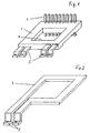
- a carrier 1 is used in which integrates one or more high-current windings 3 are.
- the high current windings 3 are located one above the other Levels in the carrier 1. This is made of plastic and is especially produced by plastic injection molding.
- the Carrier 1 has the shape of a square or rectangular Frame, as can be seen from the figures.
- the carrier 1 can also be used as a circular frame or another have the shape adapted to the application. This form is the respective high-current turn 3 adapted.
- the respective High current winding consists of a molded part that consists of a conductive material, in particular copper is formed. In it is preferably stamped parts made of copper. As can be seen from Fig. 2, the respective high current turn designed as a flat disc.
- the frame-shaped carrier 1 and the high-current windings integrated in it have a center hole 4 through which in assembled state, a central slug of a magnetic core 6 protrudes.
- the part of the magnetic core 6 protruding into the central hole 4 is covered by the high-current windings 3.
- Connections 5 in the form of connection tabs are in one piece each high-current turn 3 molded. These connections protrude laterally from the carrier 1. The connections preferably protrude 5 laterally out of a frame part of the carrier 1. The respective connections 5 run parallel to one another. When arranging several high-current turns in the carrier 1 they have a mirror image with respect to a central plane Arrangement of the leads 5 out as it can be seen in particular from FIG. 1. The high current windings can against each other by insulating coating, for example Paint must be insulated.
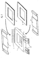
- the respective multilayer structure 7 can be designed as a standard multilayer and how from 3 can be seen on the top and the bottom of the carrier 1 can be arranged.
- the respective multilayer structure 7 contains windings in the form of copper disks or copper cladding on plastic pads or otherwise trained flat and flat ladders, which are against each other are insulated by insulating layers. It can also several multi-layer structures 7 (standard multi-layer) in stacked arrangement are used, as in the embodiment 4 is shown. In this embodiment is the stack of standard multilayers on the top the carrier 1 arranged.
- the connector pins 2 are used for receiving and connecting a Multi-layer structure (multilayers) or other winding parts.
- the connectors 2 protrude both at the top and also on the underside from the carrier. On the bottom the carrier can be connected to the motherboard the pins 2 take place. This is done with the same Pins like the contact with the winding parts of the Multi-layer construction 7.
Landscapes
- Engineering & Computer Science (AREA)
- Power Engineering (AREA)
- Coils Or Transformers For Communication (AREA)
- Coils Of Transformers For General Uses (AREA)
- Particle Formation And Scattering Control In Inkjet Printers (AREA)
- Diaphragms For Electromechanical Transducers (AREA)
- Transformers For Measuring Instruments (AREA)
Abstract
Description
Claims (13)
- Planartransformator mit Hochstromwindungen, einem Mehrschichtaufbau, dessen Schichten von flachen elektrisch leitenden Windungen und dazwischen angeordneten Isolierungen gebildet werden, einem von den Windungen umgebenen Magnetkern und einem Träger für den Mehrschichtaufbau,
dadurch gekennzeichnet, daß die Hochstromwindungen (3) jeweils voneinander isoliert in den Träger (1) mit herausgeführten elektrischen Stromanschlüssen (5) integriert sind. - Planartransformator nach Anspruch 1,
dadurch gekennzeichnet, daß die Hochstromwindungen (3) als flache Formstücke aus einem elektrisch leitfähigen Material gebildet sind. - Planartransformator nach Anspruch 2,
dadurch gekennzeichnet, daß die Hochstromwindungen (3) als Stanzteile ausgebildet sind. - Planartransformator nach einem der Ansprüche 1 bis 3,
dadurch gekennzeichnet, daß die Hochstromwindungen (3) aus Kupfer bestehen. - Planartransformator nach einem der Ansprüche 1 bis 4,
dadurch gekennzeichnet, daß die Hochstromwindungen (3) bügelförmig ausgebildet sind. - Planartransformator nach einem der Ansprüche 1 bis 5,
dadurch gekennzeichnet, daß die Hochstromwindungen (3) in unterschiedlichen Ebenen im Träger (1) angeordnet sind. - Planartransformator nach einem der Ansprüche 1 bis 6,
dadurch gekennzeichnet, daß der Träger (1) die Form eines rechteckigen, quadratischen oder kreisrunden Rahmens hat, wobei die Anschlüsse (5) der Hochstromwindungen (3) an einer Rahmenseite herausgeführt sind. - Planartransformator nach einem der Ansprüche 1 bis 7,
dadurch gekennzeichnet, daß in einem Mittelloch (4) des Trägers (1) ein von den Windungen umgebener Teil des Magnetkerns (6) angeordnet ist. - Planartransformator nach einem der Ansprüche 1 bis 8,
dadurch gekennzeichnet, daß die Hochstromwindungen durch eine isolierende Beschichtung gegeneinander isoliert sind. - Planartransformator nach einem der Ansprüche 1 bis 9,
dadurch gekennzeichnet, daß der Träger (1) aus Kunststoff besteht. - Planartransformator nach einem der Ansprüche 1 bis 10,
dadurch gekennzeichnet, daß am Träger (1) weitere Anschlußstifte (2) vorgesehen sind. - Planartransformator nach Anspruch 7 und 11,
dadurch gekennzeichnet, daß die weiteren Anschlußstifte (2) an der Rahmenseite vorgesehen sind, welcher der die Anschlüsse (5) der Hochstromwindungen (3) aufweisenden Rahmenseite entgegengesetzt liegt. - Planartransformator nach Anspruch 11 oder 12,
dadurch gekennzeichnet, daß die Anschlußstifte (2) durch den Träger (1) hindurchragen.
Applications Claiming Priority (2)
| Application Number | Priority Date | Filing Date | Title |
|---|---|---|---|
| DE19945013 | 1999-09-20 | ||
| DE19945013A DE19945013C5 (de) | 1999-09-20 | 1999-09-20 | Planartransformator |
Publications (2)
| Publication Number | Publication Date |
|---|---|
| EP1085535A1 true EP1085535A1 (de) | 2001-03-21 |
| EP1085535B1 EP1085535B1 (de) | 2009-09-09 |
Family
ID=7922640
Family Applications (1)
| Application Number | Title | Priority Date | Filing Date |
|---|---|---|---|
| EP00116058A Expired - Lifetime EP1085535B1 (de) | 1999-09-20 | 2000-07-26 | Planartransformator |
Country Status (3)
| Country | Link |
|---|---|
| EP (1) | EP1085535B1 (de) |
| AT (1) | ATE442655T1 (de) |
| DE (2) | DE19945013C5 (de) |
Cited By (3)
| Publication number | Priority date | Publication date | Assignee | Title |
|---|---|---|---|---|
| US9620278B2 (en) | 2014-02-19 | 2017-04-11 | General Electric Company | System and method for reducing partial discharge in high voltage planar transformers |
| WO2020025500A1 (de) | 2018-07-31 | 2020-02-06 | Tdk Electronics Ag | Verfahren zur herstellung eines induktiven bauelements und induktives bauelement |
| FR3109837A1 (fr) | 2020-05-04 | 2021-11-05 | Mbda France | Transformateur planaire équipé de composants, carte mère comprenant un tel transformateur planaire et procédé d’assemblage d’une telle carte mère. |
Citations (4)
| Publication number | Priority date | Publication date | Assignee | Title |
|---|---|---|---|---|
| US5010314A (en) * | 1990-03-30 | 1991-04-23 | Multisource Technology Corp. | Low-profile planar transformer for use in off-line switching power supplies |
| EP0522475A1 (de) * | 1991-07-10 | 1993-01-13 | ABBPATENT GmbH | Induktives Bauelement und Verfahren zu seiner Herstellung |
| EP0820072A1 (de) * | 1996-07-17 | 1998-01-21 | MAGNETEK S.p.A. | Flache magnetische Anordnung für elektronische Schaltungen |
| DE29907035U1 (de) * | 1999-04-20 | 1999-07-15 | Weiner, René, 51702 Bergneustadt | Spulenkörper für eine Flachspule mit einpreßbarer Stiftleiste |
Family Cites Families (10)
| Publication number | Priority date | Publication date | Assignee | Title |
|---|---|---|---|---|
| FR2476898B1 (fr) * | 1980-02-22 | 1985-06-28 | Mini Informatiq System Ste Eur | Bobinage electromagnetique comportant des elements discrets et dispositif d'alimentation electrique comportant de tels bobinages |
| JPH0613247A (ja) * | 1992-06-26 | 1994-01-21 | Fujitsu Ltd | プレーナトランス用巻線 |
| JPH0661071A (ja) * | 1992-08-11 | 1994-03-04 | Mitsubishi Electric Corp | 静止電磁誘導機器 |
| US5345670A (en) * | 1992-12-11 | 1994-09-13 | At&T Bell Laboratories | Method of making a surface-mount power magnetic device |
| EP0608127A1 (de) * | 1993-01-22 | 1994-07-27 | AT&T Corp. | Isolierungsanordnung für Magnetwindungen mit gestapelten flachen Leitern |
| US5559487A (en) * | 1994-05-10 | 1996-09-24 | Reltec Corporation | Winding construction for use in planar magnetic devices |
| EP0689214B1 (de) * | 1994-06-21 | 1999-09-22 | Sumitomo Special Metals Co., Ltd. | Herstellungsverfahren für Substrat mit mehrschichtigen gedruckten Spulen |
| EP0741395A1 (de) * | 1995-05-04 | 1996-11-06 | AT&T IPM Corp. | Anschluss-montierbare planare magnetischen Vorrichtung und ihr Herstellungsverfahren |
| AT1045U1 (de) * | 1995-10-03 | 1996-09-25 | Fronius Schweissmasch | Spulenkörper und verfahren zu dessen herstellung für einen transformator |
| JPH1012454A (ja) * | 1996-06-21 | 1998-01-16 | Toko Inc | トランスの巻線構造 |
-
1999
- 1999-09-20 DE DE19945013A patent/DE19945013C5/de not_active Expired - Lifetime
-
2000
- 2000-07-26 AT AT00116058T patent/ATE442655T1/de active
- 2000-07-26 DE DE50015737T patent/DE50015737D1/de not_active Expired - Fee Related
- 2000-07-26 EP EP00116058A patent/EP1085535B1/de not_active Expired - Lifetime
Patent Citations (4)
| Publication number | Priority date | Publication date | Assignee | Title |
|---|---|---|---|---|
| US5010314A (en) * | 1990-03-30 | 1991-04-23 | Multisource Technology Corp. | Low-profile planar transformer for use in off-line switching power supplies |
| EP0522475A1 (de) * | 1991-07-10 | 1993-01-13 | ABBPATENT GmbH | Induktives Bauelement und Verfahren zu seiner Herstellung |
| EP0820072A1 (de) * | 1996-07-17 | 1998-01-21 | MAGNETEK S.p.A. | Flache magnetische Anordnung für elektronische Schaltungen |
| DE29907035U1 (de) * | 1999-04-20 | 1999-07-15 | Weiner, René, 51702 Bergneustadt | Spulenkörper für eine Flachspule mit einpreßbarer Stiftleiste |
Cited By (7)
| Publication number | Priority date | Publication date | Assignee | Title |
|---|---|---|---|---|
| US9620278B2 (en) | 2014-02-19 | 2017-04-11 | General Electric Company | System and method for reducing partial discharge in high voltage planar transformers |
| US10236113B2 (en) | 2014-02-19 | 2019-03-19 | General Electric Company | System and method for reducing partial discharge in high voltage planar transformers |
| WO2020025500A1 (de) | 2018-07-31 | 2020-02-06 | Tdk Electronics Ag | Verfahren zur herstellung eines induktiven bauelements und induktives bauelement |
| FR3109837A1 (fr) | 2020-05-04 | 2021-11-05 | Mbda France | Transformateur planaire équipé de composants, carte mère comprenant un tel transformateur planaire et procédé d’assemblage d’une telle carte mère. |
| EP3907751A1 (de) | 2020-05-04 | 2021-11-10 | MBDA France | Grundplatine mit einem planartransformator, der mit bauteilen bestückt ist, und verfahren zum zusammenbau einer solchen grundplatine |
| WO2021224559A2 (fr) | 2020-05-04 | 2021-11-11 | Mbda France | Transformateur planaire équipé de composants, carte mère comprenant un tel transformateur planaire et procédé d'assemblage d'une telle carte mère. |
| US12243674B2 (en) | 2020-05-04 | 2025-03-04 | Mbda France | Motherboard comprising a planar transformer equipped with components and method for assembling such a motherboard |
Also Published As
| Publication number | Publication date |
|---|---|
| DE19945013C5 (de) | 2005-10-13 |
| EP1085535B1 (de) | 2009-09-09 |
| DE19945013C1 (de) | 2001-04-05 |
| ATE442655T1 (de) | 2009-09-15 |
| DE50015737D1 (de) | 2009-10-22 |
Similar Documents
| Publication | Publication Date | Title |
|---|---|---|
| EP1145610B1 (de) | Elektronisches steuergerät | |
| DE19544915C2 (de) | Elektronisches Bauteil niedrigen Profils | |
| EP0634888B1 (de) | Steckbare Baugruppe, insbesondere Relaismodul für Kraftfahrzeuge | |
| DE102009055882A1 (de) | Leistungshalbleitervorrichtung | |
| DE10148133A1 (de) | Flachtransformator mit gesteckten Sekundärwicklungen | |
| DE2205265A1 (de) | Verbinder | |
| EP0824259B1 (de) | Spulenkörper für eine Flachspule | |
| EP0177759A1 (de) | Elektronisches Bauteil, insbesondere für eine Chip-Induktivität | |
| DE19817850A1 (de) | Baugruppe mit elektronischen Bauelementen | |
| EP0995205B1 (de) | Multilayer-planarinduktivität und verfahren zum herstellen einer solchen | |
| DE69117403T2 (de) | Niederprofil-flachtransformator für die verwendung bei unabhängig betriebenen schaltnetzteilen | |
| DE10009215C1 (de) | Steckverbinder sowie Verfahren zur Herstellung eines Steckverbinders | |
| EP0173991B2 (de) | Gerätestecker mit integriertem elektrischen Entstörfilter | |
| EP1085793B1 (de) | Kompakte elektrische Vorrichtung, insbesondere Schaltnetzteil | |
| DE69729127T2 (de) | Induktives bauelement und verfahren zur herstellung eines solchen bauelements | |
| WO2008128912A1 (de) | Elektronisches bauelement | |
| DE19945013C5 (de) | Planartransformator | |
| DE102013113861A1 (de) | Galvanische Trennvorrichtung für Prozessmessgeräte | |
| EP1639869B1 (de) | Leiterplatte | |
| DE60032766T2 (de) | Electronic starter und herstellungsmethode | |
| DE202010013046U1 (de) | Transformator | |
| DE102021124211A1 (de) | Anschlussverbinder | |
| DE3340975C2 (de) | Vorrichtung zur lösbaren Montage mehrerer Schaltungsplatten auf einer Trägerplatte | |
| DE60201537T2 (de) | Elektrische verbindungsanordnung für elektronische bauteile | |
| EP1122750A1 (de) | Drossel |
Legal Events
| Date | Code | Title | Description |
|---|---|---|---|
| PUAI | Public reference made under article 153(3) epc to a published international application that has entered the european phase |
Free format text: ORIGINAL CODE: 0009012 |
|
| AK | Designated contracting states |
Kind code of ref document: A1 Designated state(s): AT DE FI SE |
|
| AX | Request for extension of the european patent |
Free format text: AL;LT;LV;MK;RO;SI |
|
| 17P | Request for examination filed |
Effective date: 20010330 |
|
| AKX | Designation fees paid |
Free format text: AT DE FI SE |
|
| RAP1 | Party data changed (applicant data changed or rights of an application transferred) |
Owner name: EPCOS AG |
|
| 17Q | First examination report despatched |
Effective date: 20061229 |
|
| GRAP | Despatch of communication of intention to grant a patent |
Free format text: ORIGINAL CODE: EPIDOSNIGR1 |
|
| GRAS | Grant fee paid |
Free format text: ORIGINAL CODE: EPIDOSNIGR3 |
|
| GRAA | (expected) grant |
Free format text: ORIGINAL CODE: 0009210 |
|
| AK | Designated contracting states |
Kind code of ref document: B1 Designated state(s): AT DE FI SE |
|
| REF | Corresponds to: |
Ref document number: 50015737 Country of ref document: DE Date of ref document: 20091022 Kind code of ref document: P |
|
| REG | Reference to a national code |
Ref country code: SE Ref legal event code: TRGR |
|
| PLBE | No opposition filed within time limit |
Free format text: ORIGINAL CODE: 0009261 |
|
| STAA | Information on the status of an ep patent application or granted ep patent |
Free format text: STATUS: NO OPPOSITION FILED WITHIN TIME LIMIT |
|
| 26N | No opposition filed |
Effective date: 20100610 |
|
| PG25 | Lapsed in a contracting state [announced via postgrant information from national office to epo] |
Ref country code: DE Free format text: LAPSE BECAUSE OF NON-PAYMENT OF DUE FEES Effective date: 20110201 |
|
| REG | Reference to a national code |
Ref country code: DE Ref legal event code: R119 Ref document number: 50015737 Country of ref document: DE Effective date: 20110201 |
|
| PGFP | Annual fee paid to national office [announced via postgrant information from national office to epo] |
Ref country code: FI Payment date: 20110727 Year of fee payment: 12 Ref country code: AT Payment date: 20110705 Year of fee payment: 12 Ref country code: SE Payment date: 20110727 Year of fee payment: 12 |
|
| REG | Reference to a national code |
Ref country code: SE Ref legal event code: EUG |
|
| REG | Reference to a national code |
Ref country code: AT Ref legal event code: MM01 Ref document number: 442655 Country of ref document: AT Kind code of ref document: T Effective date: 20120726 |
|
| PG25 | Lapsed in a contracting state [announced via postgrant information from national office to epo] |
Ref country code: SE Free format text: LAPSE BECAUSE OF NON-PAYMENT OF DUE FEES Effective date: 20120727 Ref country code: FI Free format text: LAPSE BECAUSE OF NON-PAYMENT OF DUE FEES Effective date: 20120726 |
|
| PG25 | Lapsed in a contracting state [announced via postgrant information from national office to epo] |
Ref country code: AT Free format text: LAPSE BECAUSE OF NON-PAYMENT OF DUE FEES Effective date: 20120726 |