EP1071973B1 - Verfahren zum verbinden von optischen fasern mit integrierten optischen wellenleitern - Google Patents
Verfahren zum verbinden von optischen fasern mit integrierten optischen wellenleitern Download PDFInfo
- Publication number
- EP1071973B1 EP1071973B1 EP99920625A EP99920625A EP1071973B1 EP 1071973 B1 EP1071973 B1 EP 1071973B1 EP 99920625 A EP99920625 A EP 99920625A EP 99920625 A EP99920625 A EP 99920625A EP 1071973 B1 EP1071973 B1 EP 1071973B1
- Authority
- EP
- European Patent Office
- Prior art keywords
- laser beam
- waveguide
- abutment
- zone
- laser
- Prior art date
- Legal status (The legal status is an assumption and is not a legal conclusion. Google has not performed a legal analysis and makes no representation as to the accuracy of the status listed.)
- Expired - Lifetime
Links
Images


Classifications
-
- G—PHYSICS
- G02—OPTICS
- G02B—OPTICAL ELEMENTS, SYSTEMS OR APPARATUS
- G02B6/00—Light guides; Structural details of arrangements comprising light guides and other optical elements, e.g. couplings
- G02B6/24—Coupling light guides
- G02B6/255—Splicing of light guides, e.g. by fusion or bonding
- G02B6/2551—Splicing of light guides, e.g. by fusion or bonding using thermal methods, e.g. fusion welding by arc discharge, laser beam, plasma torch
-
- G—PHYSICS
- G02—OPTICS
- G02B—OPTICAL ELEMENTS, SYSTEMS OR APPARATUS
- G02B6/00—Light guides; Structural details of arrangements comprising light guides and other optical elements, e.g. couplings
- G02B6/24—Coupling light guides
- G02B6/26—Optical coupling means
- G02B6/30—Optical coupling means for use between fibre and thin-film device
Definitions
- the present invention generally relates to the field of high-speed fiber optical communications, and more particularly to methods for joining optical fibers with integrated optical waveguides.
- optical waveguide is used herein, in distinction to the expression “optical fiber,” to designate a lightguiding medium typically formed on or in a planar (silica) substrate of rectangular cross-section (or a chip as referred to interchangeably herein).
- planar waveguide conventionally refers to a unit comprising a core and a cladding region: that is, a light path and the substrate in or on which the light path resides; however, in the present application a distinction will be made between the lightpath (“waveguide”) and the substrate (or chip) when appropriate to avoid confusion.
- the light guiding region extends to the edge or extremity of the chip.
- Waveguides of this type are frequently encountered in integrated optics applications, for example, as components of a multiplexer or demultiplexer or, more generally, as part of an integrated optical circuit.
- the conventional fusion technique for connecting optical fibers together makes use of an electric arc discharge.
- this technique is not suitable for connecting an optical fiber to a waveguide due to the geometrical characteristics of the waveguide and the heat capacity of the waveguide which is higher than that of the optical fiber.
- it has been proposed to connect an optical fiber to a planar type silica waveguide by bringing the elements into abutment and applying a laser beam to cause them to fuse together.
- a further problem arises: namely, a high energy laser beam used to create the fusion joint can cause the waveguide core to bend and, moreover, excessive melting of the optical fiber can occur.
- a lower energy laser beam is utilized, then the joint between the waveguide and the optical fiber has less strength than required for deployed applications.
- One proposed approach to solving the above problem is to pre-heat the waveguide by means other than the laser beam used for effecting the fusion between the waveguide and the optical fiber. Such pre-heating makes it possible to reduce the power of the laser beam needed to create the fusion connection.
- Such an approach complicates the process for forming the fusion joint and, in many cases, requires the use of specialised equipment and/or the modification of the structure of the integrated optical component to be connected to the optical fiber.
- multi-fiber fusion pigtailing Another consideration is the ever increasing demands being placed on an optical communications technology which have complicated the hardware and software involved, and placed great emphasis on achieving more efficient manufacture and deployment.
- the growth of metro networks and the associated signal routing, add/drop and switching requirements for narrowband WDM systems employing 16, 32, or 40 or more channels now makes it advantageous to be able to connect multiple fibers to respective waveguides (referred to hereinafter as "multi-fiber fusion pigtailing") with good performance characteristics, accuracy, repeatability and efficiency rather than single fiber/waveguide connections.
- the present invention provides a method for forming an accurate fusion joint between an optical fiber and an optical waveguide in a chip, with low optical losses and a strong joint.
- the invention further provides a method for accurately performing multi-fiber fusion pigtailing between multiple fibers and multiple waveguides on a chip, with low optical losses and strong joints.
- the invention provides a method for connecting an optical fiber to an optical waveguide in a chip, comprising the steps of:
- One preferred way of so modifying the spatial energy distribution involves interposing a shield element in the path of the laser beam upstream of the zone of abutment in order to eliminate a substantially central part of the laser beam while allowing a peripheral part thereof to pass.
- Another preferred way of reducing the energy in the substantially central part of the spatial energy distribution with respect to the peripheral part comprises dividing the laser beam, upstream of the zone of abutment, into several distinct beams, and directing these beams towards the zone of abutment. This can be done, for example, by a splitting mirror disposed in the path of the laser beam upstream of the zone of abutment, with the distinct beams directed towards the zone of abutment by parabolic mirrors.
- the distinct beams resulting from the splitting of the laser beam can be slightly defocused at the zone of abutment.
- the invention also includes a method for connecting a plurality of optical fibers to a respective plurality of waveguides in a chip, as defined in claim 20.
- Such method thus comprises the steps of propagating a substantially collimated laser beam through a diffractive optical element (DOE) to simultaneously produce a desired spatial laser energy distribution at a zone of abutment for each of the fiber-waveguide connections.
- DOE diffractive optical element
- the invention described herein provides a method for strongly, accurately, and efficiently connecting an optical fiber to a waveguide in an optical chip.
- the energy distribution at the zone of abutment can be asymmetrical; that is, the energy impinging upon the waveguide can be greater than that which reaches the optical fiber. In this way, the degree of melting of the optical fiber can be controlled.
- the invention further includes a method of connecting a plurality of optical fibers to a respective plurality of waveguides in a chip, comprising the steps of
- a force is applied between the optical fiber and the waveguide in a direction moving the optical fiber and waveguide closer together during irradiation of the zone of abutment.
- the power cycle of the laser is controlled such that the laser beam power is held at a first, relatively higher level during a first period of time during which the fusion joint is created, and it maintained at a lower level during a second period of time, allowing gradual cooling of the fusion joint.
- the methods of the present invention find application in connecting optical fibers to planar silica waveguides.
- the irradiation step is performed using a laser beam of wavelength greater than 4 ⁇ m.
- Suitable lasers include a CO laser having a wavelength of 9.8 ⁇ m, and a CO 2 laser having a wavelength of 10.6 ⁇ m. Use of a CO 2 laser currently provides a cost advantage.
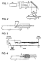
- An exemplary embodiment of the method for connecting an optical fiber to an optical waveguide formed in a chip according to the present invention can be put into practice using the method described herein in conjunction with the apparatus illustrated in Figure 1.
- This apparatus and method are used to form a fusion joint between a silica waveguide 1a provided on a silica substrate 1 (constituting an integrated optics chip) and the end 3 of an optical fiber 2 aligned with the waveguide 1a.
- the end 3 of the optical fiber 2 is stripped, i.e. the sheath protecting the latter is removed to expose the silica part of the fiber.
- the end of the chip 1 preferably has a stepped portion 5 to accommodate the stripped end 3 and the non-stripped portion of the optical fiber 2.
- a CO 2 laser 10 generates a laser beam which is expanded and collimated by a component 12, reflected by a mirror 14 and focused by a lens (or lens system) 16.
- the laser beam is focused substantially onto the interface 4 between the optical fiber and the waveguide, hereinafter referred to interchangeably as the zone of abutment or interface.
- the energy furnished by the laser beam to the zone of abutment 4 between the waveguide 1a and the stripped end 3 of the optical fiber 2 presents a spatial distribution in which the energy corresponding to a substantially central part thereof is lower than that corresponding to a peripheral part, as illustrated in Figure 6C.
- substantially central part is understood to mean a central zone or one slightly offset relatively to the center of the energy distribution of the beam.
- a beam blocking or shield element 20 of preferably substantially cylindrical shape is disposed in the path of the laser beam advantageously after enlargement and collimation by component 12 but before focusing by element 16.
- the energy density falling upon the shield element 20 is lower than in the case where the shield element were to be positioned before the magnification unit or after the focusing lens 16.
- This placement reduces local heating effects in the shield member 20.
- the shield element 20 by locating the shield element 20 at a point in the optical path of the laser beam where the diameter thereof is relatively great, there is increased accuracy in the centering of the shield element 20 with respect to the laser beam.
- the shield element 20 is located between the magnification unit 12 and the mirror 14 but, in another aspect, it could be located between the mirror 14 and lens 16.
- the shield element 20 prevents a substantially central part 17 of the laser beam emitted by the laser 10 to reach the interface 4.
- the shield element 20 eliminates the energy corresponding to this substantially central part 17, while letting the remaining peripheral part 18 of the beam propagate towards the interface 4.
- the shielding or blocking of the central part 17 of the laser beam makes it possible to eliminate a high proportion of the energy in the central portion of the beam.
- the diameter and the position of the shield element 20 are selected such that 20 to 80% of the energy of the beam emitted by the laser 10, and more preferably about 50% of the energy, is prevented from reaching the elements intended to be fused at the interface 4.
- the shield element 20 should have good thermal conductivity so that it can dissipate the significant energy produced by the laser beam.
- the length of the shield element 20 is selected to be as great as is practically possible, in view of the desired size of the whole device, in order to optimise energy dissipation therein.
- the diameter and the length of the element 20 are 5mm and 10mm, respectively.
- the material of the shield element has a low deformation when it is heated in order to ensure that the quantity of energy eliminated from the laser beam and the spatial distribution of the remaining energy are stable and reproducible. Steel and carbon are suitable exemplary materials for element 20.
- the chip 1 incorporating the waveguide 1a, and the optical fiber 2 are mounted on respective micro-positioning stages (not shown), positioned to abut against one another and aligned in a conventional manner (typically by a conventional method which maximises light transmitted between the optical fiber and the waveguide) as illustrated in Figure 2.
- a conventional manner typically by a conventional method which maximises light transmitted between the optical fiber and the waveguide
- the chip and fiber are positioned with respect to the laser beam as described in greater detail below.
- the CO 2 laser 10 is activated so as to generate, at a first, higher power level, a laser beam having a beam diameter of about 3.5mm which is expanded by the magnifying/collimating component 12 to a diameter of about 14mm, reflected by the mirror 14 and focused by the lens (or the lens system) 16 substantially on the interface, or zone of abutment, 4 between the optical fiber 3 and the waveguide 1a.
- the diameter of the laser beam after focusing by the element 16 is typically of the order of 150-400 ⁇ m.
- the laser beam is preferably slightly defocused at the zone of abutment 4, in order to render the spot produced by the beam slightly blurred at this zone.
- the shield element 20 Due to the presence of the shield element 20 in the optical path of the laser beam, approximately 50% of the beam energy produced by the laser 10 is prevented from propagating towards the elements to be fused.
- a relatively high power laser beam can be used in the process without causing bending of the waveguide core.
- the spot produced by the laser beam at the zone of abutment 4 is not strictly centered on the boundary of the optical fiber 2 and the waveguide 1a, but instead is offset in the direction towards the waveguide by a distance ⁇ x. This offset ensures that a greater fraction of the beam energy reaches the waveguide 1a than the optical fiber 2 which, due to its specific heat capacity being lower than that of the waveguide, would tend to melt to an undesirable degree.
- the offset ⁇ x should be between about 20-60 ⁇ m. Such a value of the offset ensures that the desired temperature distribution is effected. In particular, it is thus possible to take the waveguide and the optical fiber to the same temperature.
- the laser beam is set at a first power level which is relatively high in order to cause local melting of the waveguide 1a and optical fiber end 3 at the boundary 4, as shown in Figure 3.
- a force, F is applied so as to exert a gentle pressure urging the optical fiber towards the waveguide.
- the force F may be applied on the waveguide, or complementary forces may be applied on the waveguide and optical fiber 2.
- the end 3 of the optical fiber 2 deforms upon melting so as to create an empty space between the optical fiber and the waveguide.
- application of the force F is desirable in order to produce a strong fusion joint with low optical losses.
- FIG. 1 illustrates a typical power cycle of the CO 2 laser during a cycle of the method according to the present invention.
- Figure 3 also indicates the time period during which the application of force F causes movement of the fiber 2 towards the waveguide 1a, and the level of an optical signal transmitted between the fiber 2 and waveguide 1a for purposes of monitoring the progression of the connection process. It can be seen that the various steps of the connection cycle are very short. Therefore it is preferred that the displacements of the micro-positioning stages, and the power cycle of the laser, be computer-controlled. Typically, the power cycle of the laser is controlled by controlling the excitation current thereof using a control signal. Conventionally, the level of this control signal can in turn be fixed by varying a regulation current or voltage, depending upon the detailed implementation of the control unit, all of which is understood by those skilled in the art.
- the desired distribution can be achieved using a shield element 20 whose cross sectional shape (perpendicularly to the laser beam 17, 18) is such that the laser beam comprises more energy at positions which will be focused onto the waveguide and relatively less energy at positions that will be focused onto the optical fiber 2.
- a shielding element 20 could, for example, be pear-shaped in cross section.
- the desired temperature distribution could be obtained by a combination of an offset of the laser beam and the use of a specially-shaped shielding element 20.
- Shielding elements other than those described hereinabove may also be used for eliminating part of the energy of the laser beam.
- another element of circular cross-section such as a cone
- elements not presenting a circular cross-section may be used: for example, elements whose section is in the form of a star, ellipsis, etc.
- a shield of circular shape or of different shape
- substantially in two dimensions or a thin shielding element such as a disc.
- a laser other than a CO 2 laser may be used as long as the material of the waveguide is capable of absorbing energy at the wavelength of the laser.
- this condition implies in practice that the wavelength of the laser is greater than about 4 ⁇ m.
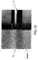
- a method for accurately positioning the laser beam at the zone of abutment is described with reference to Figures 8-10.
- a camera 108 that is fixed in position while imaging, relative to the chip 1 and the fiber end 3 to be fused together, provides an image in a field of view 110 surrounding and including the zone of abutment 4 between the waveguide and the optical fiber.
- a low power laser beam from the CO 2 laser is focused on the chip within the field of view and image recognition software, such as, e.g., OptimasTM by Imasys, is utilized to generate a set of coordinates X 1 , Y 1 corresponding to the position of substantially the center of the focused laser beam 18.
- the initial location of the beam denoted by X 1 , Y 1 is set off from a border (or extremity) 112 of the chip 1 and the waveguide 2 by an amount ⁇ X, ⁇ Y respectively.
- the extremity of the waveguide is also identified and denoted by a set of co-ordinates X 2 , Y 2 .
- ⁇ X is preferably about 300 ⁇ m.
- ⁇ Y is preferably about 175 ⁇ m along a Y-axis normal to the X-axis. It will be appreciated, however, that ⁇ Y will be motivated by the waveguide pitch in all such cases.
- a first image was obtained over a time of about 2-3 seconds, and four subsequent images were obtained at approximately 0.4 seconds after each preceding image.
- This method allowed the extremity of the waveguide to be positioned to within about ⁇ 1 ⁇ m with respect to the approximate laser beam center at the zone of abutment.
- Figure 10 shows a marker identifying the extremity 112 of the waveguide 1 and the optical fiber end 3.
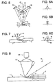
- a laser beam 40 produced by a laser source (not shown) is directed towards a splitting mirror 50 which splits the beam 40 into two distinct laser beams 41 and 42.
- Each beam 41, 42 is then reflected by a respective parabolic mirror 60, 70 and focused by this parabolic mirror on the interface 4 between the optical fiber 2 and the waveguide 1a.
- the splitting mirror 50 is preferably in the form of a triangular prism, of which a median line of the triangular cross-section (in the plane of Figure 5) substantially merges with the axis 43 of the laser beam 40, and of which two adjacent side faces 51, 52 disposed one either side of the axis 43 are reflecting.
- the laser beams 41 and 42 reflected respectively by the faces 51, 52 of the splitting mirror 50 are preferably focused by the parabolic mirrors on the zone of abutment 4 between the optical fiber end 3 and the waveguide 1a so as to be superposed thereon.
- Figure 6 illustrates the modification of the distribution of energy of the laser beam 40 by the optical elements 50, 60 and 70 during irradiation of the zone of abutment between the optical fiber 2 and the waveguide 1a.
- the Gaussian profile (cf. Figure 6A) of the energy distribution of the laser beam 40, in a plane perpendicular to that of Figure 5, before splitting of the beam by the splitting mirror 50, is transformed at the zone of abutment into a substantially rectangular energy profile, shown in broken lines in Figure 6B.
- This substantially rectangular profile corresponds to the sum of two Gaussian half-curves respectively associated with the two beams 41, 42.
- the profile of the energy distribution at the zone of abutment 4 between the optical fiber 2 and the waveguide 1a as shown in Figure 6B therefore presents a central part of which the level of energy has been reduced to become of the same order as that of the remaining peripheral part. In this way, the presence of a maximum of energy at the center of this distribution is avoided.
- the profile of distribution of energy at the zone of abutment is not necessarily rectangular.
- Figure 6C shows another example of distribution of energy in which the energy corresponding to a substantially central zone 80 of the energy distribution has been reduced with respect to the remaining peripheral part, i.e. the edges, 81 thereof. In the exemplary profile of Figure 6C, the energy at the edges 81 is greater than that at center 80.
- Such a profile is obtained in this embodiment by applying the two laser beams 41, 42 to two different spots at the zone of abutment 4, as shown in Figure 7.
- the distribution profile shown in Figure 6C is substantially the same as that obtained in the first embodiment with the aid of the shielding element 20.
- the effect produced in the zone of abutment 4 by the energy distributions of Figures 6B and 6C is not very different since, in the case of a distribution of the type of Figure 6C, the temperature distribution in the zone of abutment between the optical fiber 2 and the waveguide 1a is substantially homogeneous due to the thermal diffusion which is produced in this zone of abutment.
- the laser beams 41, 42 irradiating the zone of abutment 4 between the optical fiber 2 and the waveguide 1a are slightly defocused at this zone of abutment, in order to render the spot produced by the beams 41, 42 slightly blurred at the zone 4. In this way it is possible to spread the energy distribution so as to render the latter more homogeneous.
- the beams 41, 42 are preferably applied on the zone of abutment 4 so that the quantity of energy reaching the waveguide 1a is greater than that reaching the optical fiber 2.
- the beams 41, 42 are directed towards the zone of abutment 4 so that the spot produced thereby at zone 4 is offset with respect to the boundary between the waveguide 1a and the optical fiber 2, in a direction towards the waveguide.
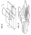
- Another preferred embodiment of the invention describes a method for connecting a plurality of optical fibers to a respective plurality of waveguides in a chip, that is, multi-fiber fusion pigtailing, and is described below with reference to Figures 11-13.
- a silica chip 1 incorporating a number of waveguides 1a to be connected at an extremity 112 of the chip to a respective number of stripped ends 3 of optical fibers 2 is illustrated.
- a respective number of laser beams 120 are shown irradiating the zones of abutment 4 between the waveguides and the fibers.
- a diffractive optical element (DOE) 130 as shown in Figure 13 is inserted in the path of the expanded and collimated laser beam.
- DOE 130 diffractive optical element
- any desired wavefront or series of wavefronts can be generated resulting in a preferred intensity distribution of the beam at the zones of abutment 4.
- Figures 12A, 12B, 12C and 12D illustrate four different possible beam distributions produced by the DOE 130 including a uniform rectangular distribution 12A; a rectangular distribution having a quasi-Gaussian profile wherein the intensity between the tails and the central portion of the profile varies between about 1 to 10% 12B; a series of square distributions 12C; and a series of circular distributions 12D, the latter two of which have a periodicity or pitch corresponding to that of the fiber/waveguides.
- the profile represented by 12B is preferred with respect to that of 12A for irradiating chips having a relatively smaller width because of the greater influence of the chip border in a smaller chip on the heat diffusion from the laser beam.
- Chips of relatively greater width have a less significant influence on the heat diffusion arising from chip border considerations making the profile 12A more advantageous for use with large chips.
- optimized wavefronts can be generated which meet the fusion temperature requirements and the spatial energy distributions at the zones of abutment to fuse the joints while not adversely melting the fiber or warping the substrate as identified above as problems associated with conventional laser fusion methods.
- a CO 2 laser 10 generates a beam that is expanded and collimated by component 12.
- the collimated beam is propagated to a reflecting element 140 and then through a DOE 130 which produces a desired intensity distribution at the zones of abutment 4 for multi-fiber fusion pigtailing a series of optical fibers 2 and waveguides 1a in a silica chip 1.
- the DOE 130 provides the additional function of focusing the beam at the zones of abutment or at least providing a slightly defocused beam as may be suitable for attaining the desired energy distribution at the zones of abutment.
- the focusing function may be performed by an additional appropriate lens element, such as a ZnSe lens (not shown) positioned upstream of the DOE.
- a coordinate X 1 corresponding to the position of substantially a center of the beam along an X-axis parallel to the waveguide in the chip, wherein X 1 is set off from a border of the chip and the waveguide, respectively, by an amount ⁇ X.
- the extremity of the waveguide along the X-axis is assigned the coordinate X 2 .
- Positioning of the beam according to the method described herein provides a positioning accuracy of ⁇ 1 ⁇ m or better. Such positioning accuracy assured good reproducibility of the heated area of the zone of abutment which is critical because of the large thermal capacity difference between the silica chip and the optical fiber.
- a laser beam 10 from a CO 2 laser is incident on a beam scanner 170 which may comprise, for example, one or more movable mirrors which provide beam steering at least in orthogonal X and Y directions.
- the beam 10 is expanded and collimated by component 12 and directed to scanner 170.
- scanner 170 further comprises components (not shown) such as a lens or lens system for beam shaping, focusing, wavefront manipulation or other beam processing for optimal irradiation of the chip 1.
- scanner 170 is separate from a lens or lens system depicted by reference 172.
- all fiber/waveguide connections are substantially simultaneously heated by the scanning laser beam.
- a typical scanning frequency is on the order of 100Hz-10kHz.
- Positioning of the chip/waveguide with respect to the laser spot is substantially to the method described above for the single fusion case.
- the laser beam spot size is the same as in the single fusion case.
- the coordinates of the beam center, the waveguide extremity and the offset are calculated and processed as in the single fusion case.
Landscapes
- Physics & Mathematics (AREA)
- General Physics & Mathematics (AREA)
- Optics & Photonics (AREA)
- Engineering & Computer Science (AREA)
- Plasma & Fusion (AREA)
- Optical Couplings Of Light Guides (AREA)
- Laser Beam Processing (AREA)
Claims (27)
- Verfahren zur Verbindung einer optischen Faser (3) mit einem optischen Wellenleiter (1a) in einem Chip (1) mit folgenden Schritten:dadurch gekennzeichnet, dass die räumliche Energieverteilung des Laserstrahls derart modifiziert wird, dass der zentrale Abschnitt der Verteilung über dem Berührungsbereich zwischen der optischen Faser und dem Wellenleiter bezüglich des zentralen Abschnitts davon am Laserausgang zum Verhindern eines nachteiligen Schmelzens der optischen Faser oder eines Biegens des Wellenleiters verringert wird.Ausrichten der optischen Faser mit dem Wellenleiter;miteinander In-Berührung-Bringen der optischen Faser und des Wellenleiters;Aussenden eines Laserstrahls von einem Laser (10); undBestrahlen eines Bereiches um die sich berührende optische Faser und den Wellenleiter herum mit dem Laserstrahl, wodurch die optische Faser mit dem Wellenleiter verschmolzen wird,
- Verfahren nach Anspruch 1,
dadurch gekennzeichnet, dass der Schritt des Modifizierens der räumlichen Energieverteilung ferner den Schritt aufweist: Anordnen einer Abschirmung (20) in dem Ausbreitungsweg des Laserstrahls stromaufwärts des Berührungsbereiches zum Ausblenden eines wesentlichen zentralen Abschnitts des Laserstrahls, während ein umfänglicher Abschnitt davon passieren kann. - Verfahren nach Anspruch 2,
dadurch gekennzeichnet, dass zwischen 20 Prozent und 80 Prozent der Leistung des Laserstrahls durch die Abschirmung stromaufwärts des Berührungsbereiches zwischen der optischen Faser und dem Wellenleiter ausgeblendet wird. - Verfahren nach Anspruch 2,
dadurch gekennzeichnet, dass ungefähr 50 Prozent der Leistung des Laserstrahls durch die Abschirmung ausgeblendet wird. - Verfahren nach wenigstens einem der vorhergehenden Ansprüche,
dadurch gekennzeichnet, dass der Schritt des Bestrahlens des Berührungsbereiches ferner den Schritt aufweist: Fokussieren des Laserstrahls im Wesentlichen auf den Berührungsbereich. - Verfahren nach einem der Ansprüche 1 bis 4,
dadurch gekennzeichnet, dass der Schritt des Bestrahlens des Berührungsbereiches ferner den Schritt aufweist: leichtes Defokussieren des Strahls auf dem Berührungsbereich. - Verfahren nach einem der Ansprüche 2 bis 4,
dadurch gekennzeichnet, dass die Abschirmung (20) im Wesentlichen eine zylindrische Form aufweist und dass eine Längsachse des Zylinders in dem Ausbreitungsweg des Laserstrahls angeordnet ist, wobei die Achse in einer Propagationsrichtung des Laserstrahls ausgerichtet wird. - Verfahren nach Anspruch 1,
dadurch gekennzeichnet, dass die räumliche Energieverteilung des Laserstrahls (40) durch Aufteilung des Laserstrahls in mehrere Strahlen (41, 42) stromaufwärts des Berührungsbereiches und Ausrichten der aufgeteilten Strahlen in Richtung des Berührungsbereiches modifiziert wird. - Verfahren nach Anspruch 8,
dadurch gekennzeichnet, dass mehrere Strahlen an dem Berührungsbereich leicht defokussiert werden. - Verfahren nach wenigstens einem der vorhergehenden Ansprüche,
dadurch gekennzeichnet, dass die räumliche Energieverteilung derart ausgestaltetwird, dass die Menge an Energie, welche den Wellenleiter bestrahlt, größer ist als die Menge, welche die optische Faser bestrahlt. - Verfahren nach wenigstens einem der vorhergehenden Ansprüche,
dadurch gekennzeichnet, dass der Schritt des Bestrahlens des Berührungsbereiches ferner den Schritt aufweist: Ausbilden des Laserstrahls an dem Berührungsbereich mit einem-bestimmten Durchmesser, wobei der Strahl ferner bezüglich eines Grenzbereichs zwischen der optischen Faser und dem Wellenleiter versetzt ist, nämlich in Richtung des Wellenleiters mit einem Abstand von ungefähr 5 bis 20 Prozent des Durchmessers. - Verfahren nach wenigstens einem der vorhergehenden Ansprüche,
dadurch gekennzeichnet, dass während der Bestrahlung des Berührungsbereiches eine Kraft zwischen der optischen Faser und dem Wellenleiter angelegt wird, um diese näher zusammenzubewegen. - Verfahren nach Anspruch 12,
dadurch gekennzeichnet, dass die Kraft eine relative Verschiebung verursacht, die kleiner oder gleich 50 µm ist. - Verfahren nach wenigstens einem der vorhergehenden Ansprüche,
dadurch gekennzeichnet, dass es ferner folgenden Schritt aufweist: Bilden einer weiteren Verbindung zwischen der optischen Faser und dem Wellenleiter unter Verwendung eines Haftmittels (25). - Verfahren nach wenigstens einem der vorhergehenden Ansprüche,
dadurch gekennzeichnet, dass die Laserleistung auf ein erstes relativ hohes Niveau während eines ersten Zeitraums gesetzt wird, währenddessen eine Schmelzverbindung zwischen der optischen Faser und dem Wellenleiter gebildet wird, und auf ein niedrigeres Niveau während eines zweiten Zeitraums gesetzt wird, im Anschluss an den ersten Zeitraum, um eine- schrittweise Abkühlung der Schmelzverbindung zu ermöglichen. - Verfahren nach wenigstens einem der vorhergehenden Ansprüche,
dadurch gekennzeichnet, dass der Wellenleiter in einem Siliciumchip gebildet wird. - Verfahren nach wenigstens einem der vorhergehenden Ansprüche,
dadurch gekennzeichnet, dass der Laserstrahl eine Wellenlänge aufweist, die größer als 4 µm ist. - Verfahren nach Anspruch 17,
dadurch gekennzeichnet, dass als Laser ein CO2-Laser verwendet wird. - Verfahren nach wenigstens einem der vorhergehenden Ansprüche,
dadurch gekennzeichnet, dass ein äußerstes Ende des Wellenleiters innerhalb ungefähr ± 1µm bezüglich der Mitte des Laserstrahls an dem Berührungsbereich positioniert wird. - Verfahren zur Verbindung mehrerer optischer Fasern (2) mit entsprechenden mehreren Wellenleitern (1a) in einem Chip (1) mit folgenden Schritten:dadurch gekennzeichnet, dass der Laserstrahl durch ein optisches Brechungselement (140) propagiert wird, um gleichzeitig eine gewünschte räumliche Laserenergieverteilung an dem Berührungsbereich für jede der mehreren Verbindungen zu erzeugen und um eine nachteilige Verschmelzung der optischen Fasern oder eine Biegung der Wellenleiter zu verhindern.Ausrichten der optischen Fasern mit den entsprechenden Wellenleitern;miteinander In-Berührung-Bringen der optischen Fasern mit den entsprechenden Wellenleitern;Aussenden eines Laserstrahls von einem Laser; undBestrahlen eines Bereiches um die sich berührenden optischen Fasern und Wellenleiter herum mit dem Laserstrahl, wodurch die optischen Fasern mit den entsprechenden Weilenleitern verschmolzen werden;
- Verfahren nach Anspruch 20,
dadurch gekennzeichnet, dass die räumliche Energieverteilung des Laserstrahls auf dem Chip durch eine zweidimensionale Form gebildet wird, welche wenigstens aus einer der nachfolgenden Formen gebildet ist, nämlich einer rechteckigen, einer Reihe von quadratischen oder einer Reihe von kreisrunden Formen. - Verfahren nach Anspruch 20 oder 21,
dadurch gekennzeichnet, dass das optische Brechungselement von der fokussierenden Linse stromabwärts angeordnet wird. - Verfahren nach wenigstens einem der Ansprüche 20 bis 22,
dadurch gekennzeichnet, dass das optische Brechungselement für eine Fokussierung des Laserstrahls auf dem Chip verwendet wird. - Verfahren nach wenigstens einem der Ansprüche 20 bis 23,
dadurch gekennzeichnet, dass der Laserstrahl mit einer Wellenlänge ausgebildet wird, die größer oder gleich 4 µm ist. - Verfahren nach Anspruch 24,
dadurch gekennzeichnet, dass der Laser als CO2-Laser ausgebildet wird. - Verfahren zur Verbindung mehrerer optischer Fasern (2) mit entsprechenden mehreren Wellenleitern (12) in einem Chip (1) mit folgenden Schritten:dadurch gekennzeichnet, dass der Laserstrahl zu einem Strahlscanner (17) propagiert wird und zum Abtasten über die Berührungsbereiche zwischen den optischen Fasern und den entsprechenden Wellenleitern mit einer bestimmten räumlichen Energieverteilung und einer Wiederholungsrate modifiziert wird, wodurch die mehreren Berührungsbereiche im Wesentlichen gleichzeitig erhitzt werden und eine nachteilige Verschmelzung der optischen Fasern oder eine Biegung der Wellenleitern vermieden wird.Ausrichten der optischen Fasern mit den entsprechenden Wellenleitern;miteinander In-Berührung-Bringen der optischen Fasern und der entsprechenden Wellenleitern;Aussenden eines Laserstrahls von einem Laser; undBestrahlen eines Bereiches um die sich berührenden optischen Fasern und Wellenleiter herum mit dem Laserstrahl, wodurch die optischen Fasern mit den entsprechenden Wellenleitern verschmolzen werden;
- Verfahren nach Anspruch 26,
dadurch gekennzeichnet, dass der Strahl mit einer Wiederholungsrate zwischen ungefähr 100 Hz bis 10 kHz abgetastet wird.
Applications Claiming Priority (3)
| Application Number | Priority Date | Filing Date | Title |
|---|---|---|---|
| FR9804438A FR2777359B1 (fr) | 1998-04-09 | 1998-04-09 | Connexion d'une fibre optique et d'un guide d'ondes optique par fusion |
| FR9804438 | 1998-04-09 | ||
| PCT/EP1999/002421 WO1999053351A1 (en) | 1998-04-09 | 1999-04-09 | Method for connecting optical fiber and optical waveguide |
Publications (2)
| Publication Number | Publication Date |
|---|---|
| EP1071973A1 EP1071973A1 (de) | 2001-01-31 |
| EP1071973B1 true EP1071973B1 (de) | 2003-09-24 |
Family
ID=9525053
Family Applications (1)
| Application Number | Title | Priority Date | Filing Date |
|---|---|---|---|
| EP99920625A Expired - Lifetime EP1071973B1 (de) | 1998-04-09 | 1999-04-09 | Verfahren zum verbinden von optischen fasern mit integrierten optischen wellenleitern |
Country Status (10)
| Country | Link |
|---|---|
| US (1) | US6411759B1 (de) |
| EP (1) | EP1071973B1 (de) |
| JP (1) | JP2002511599A (de) |
| CN (1) | CN1295676A (de) |
| AU (1) | AU3814499A (de) |
| CA (1) | CA2327428A1 (de) |
| DE (1) | DE69911593D1 (de) |
| FR (1) | FR2777359B1 (de) |
| TW (1) | TW424165B (de) |
| WO (1) | WO1999053351A1 (de) |
Families Citing this family (25)
| Publication number | Priority date | Publication date | Assignee | Title |
|---|---|---|---|---|
| EP1174740A1 (de) * | 2000-07-21 | 2002-01-23 | Corning Incorporated | Verfahren und Vorrichtung zum Spleissen von optischen Fasern mit unterschiedlichen Modenfelddurchmessern |
| EP1255139A1 (de) * | 2001-05-03 | 2002-11-06 | Corning Incorporated | Verfahren und Apparat zum Spleissen von Glasfasern |
| DE10127331B4 (de) * | 2001-05-22 | 2006-06-14 | Schott Ag | Verfahren zum Verbinden mindestens einer optischen Faser mit einer GRIN-Linse und Filtermodul |
| TW552645B (en) * | 2001-08-03 | 2003-09-11 | Semiconductor Energy Lab | Laser irradiating device, laser irradiating method and manufacturing method of semiconductor device |
| GB0129286D0 (en) * | 2001-12-06 | 2002-01-23 | Optek Ltd | Improvements relating to the coupling of optical waveguides |
| SE522255C2 (sv) * | 2002-02-26 | 2004-01-27 | Ericsson Telefon Ab L M | Anordning och förfarande för smältskarvning av ändar av två optiska fibrer |
| DE10234946A1 (de) * | 2002-07-31 | 2004-02-19 | CCS Technology, Inc., Wilmington | Verfahren und Vorrichtung zum Spleißen von Lichtwellenleitern |
| GB0223361D0 (en) * | 2002-10-08 | 2002-11-13 | Council Cent Lab Res Councils | Optical micro sensor |
| US20040071404A1 (en) * | 2002-10-09 | 2004-04-15 | Masalkar Prafulla Jinendra | Apparatus for increasing directivity and lowering background light in tap detectors |
| US20050180695A1 (en) * | 2002-10-15 | 2005-08-18 | Sagitta Engineering Solutions Ltd. | Method and apparatus for planar lightwave circuits pigtailing |
| US20050135733A1 (en) * | 2003-12-19 | 2005-06-23 | Benoit Reid | Integrated optical loop mirror |
| US7263260B2 (en) * | 2005-03-14 | 2007-08-28 | Matsushita Electric Industrial Co., Ltd. | Low cost, high precision multi-point optical component attachment |
| WO2008032165A2 (en) * | 2006-09-12 | 2008-03-20 | Kilolambda Technologies Ltd. | A method for laser induced fusion pigtailing of optical fiber to optical waveguide |
| JP2008242012A (ja) * | 2007-03-27 | 2008-10-09 | Mitsubishi Cable Ind Ltd | レーザーガイド用光ファイバ及びそれを備えたレーザーガイド |
| JP4682179B2 (ja) * | 2007-11-19 | 2011-05-11 | 三菱電機株式会社 | 樹脂材の溶着方法及び溶着装置 |
| KR102493498B1 (ko) * | 2013-11-27 | 2023-01-27 | 매직 립, 인코포레이티드 | 가상 및 증강 현실 시스템들 및 방법들 |
| JP6417710B2 (ja) * | 2014-05-20 | 2018-11-07 | 住友電気工業株式会社 | 屈曲光ファイバ製造方法 |
| CN110045463B (zh) * | 2018-01-15 | 2021-09-07 | 中国科学院上海光学精密机械研究所 | 一种光纤熔接的连接件与方法 |
| US10345533B1 (en) * | 2018-02-15 | 2019-07-09 | Corning Incorporated | Assemblies, optical connectors and methods of bonding optical fibers to substrates |
| US10746937B2 (en) * | 2018-02-15 | 2020-08-18 | Corning Incorporated | Assemblies, optical connectors and methods of bonding optical elements to substrates |
| US11701839B2 (en) * | 2018-06-14 | 2023-07-18 | Airbus Operations Gmbh | Method and system for joining two components of a meltable material |
| US11808981B2 (en) | 2018-07-06 | 2023-11-07 | O'fiberty Technologies Inc. | Method of fusion splicing optical fibers with lasers |
| US11841535B2 (en) | 2018-07-06 | 2023-12-12 | O'fiberty Technologies Inc. | Method of fusion splicing optical fibers with lasers |
| CN109954969B (zh) * | 2019-03-29 | 2021-04-13 | 中国航空制造技术研究院 | 激光深熔焊接和激光修饰焊接的柔性切换方法 |
| US20230019700A1 (en) * | 2019-12-19 | 2023-01-19 | Soreq Nuclear Research Center | Optical fibers fusion-splicing to waveguides |
Family Cites Families (16)
| Publication number | Priority date | Publication date | Assignee | Title |
|---|---|---|---|---|
| NL8700716A (nl) * | 1987-03-26 | 1988-10-17 | Advanced Prod Automation | Vezelinkoppelinrichting voor laserenergie. |
| JP2580741B2 (ja) * | 1988-10-24 | 1997-02-12 | 日立電線株式会社 | 導波路形光モジュール |
| DE3912237A1 (de) * | 1989-04-14 | 1990-10-18 | Zeiss Carl Fa | Spiegel zur veraenderung der geometrischen gestalt eines lichtbuendels |
| US5138490A (en) * | 1989-04-29 | 1992-08-11 | Carl-Zeiss-Stiftung | Arrangement for changing the geometrical form of a light beam |
| JPH0328806A (ja) * | 1990-04-19 | 1991-02-07 | Nippon Telegr & Teleph Corp <Ntt> | 光導波路と光ファイバとの結合方法 |
| US5208885A (en) * | 1992-02-27 | 1993-05-04 | At&T Bell Laboratories | Optical fiber to strip waveguide interconnect |
| US5315095A (en) * | 1993-02-18 | 1994-05-24 | Symbol Technologies, Inc. | Beam with extended confinement for scanning purposes |
| WO1994029760A1 (en) * | 1993-06-04 | 1994-12-22 | Summit Technology, Inc. | Rotatable aperture apparatus and methods for selective photoablation of surfaces |
| JP3531199B2 (ja) * | 1994-02-22 | 2004-05-24 | 三菱電機株式会社 | 光伝送装置 |
| JPH07294770A (ja) * | 1994-04-28 | 1995-11-10 | Hitachi Cable Ltd | 石英系導波路と光ファイバとの接続方法および接続部構造 |
| JPH0875949A (ja) * | 1994-09-08 | 1996-03-22 | Hitachi Cable Ltd | ガラス導波路と光ファイバとの融着接続方法及び融着接続装置 |
| AUPN089895A0 (en) * | 1995-02-03 | 1995-03-02 | University Of Sydney, The | Broadband grating |
| JP3456809B2 (ja) * | 1995-10-30 | 2003-10-14 | シャープ株式会社 | 光導波路素子、光導波路素子への結合方法、光ピックアップ装置 |
| JP3348345B2 (ja) * | 1997-08-29 | 2002-11-20 | 株式会社豊田中央研究所 | レーザによる溝加工方法 |
| US6033515A (en) * | 1998-07-17 | 2000-03-07 | Lightpath Technologies, Inc. | Use of a laser to fusion-splice optical components of substantially different cross-sectional areas |
| JP3526224B2 (ja) * | 1998-10-20 | 2004-05-10 | シャープ株式会社 | 加工方法および光学部品 |
-
1998
- 1998-04-09 FR FR9804438A patent/FR2777359B1/fr not_active Expired - Fee Related
-
1999
- 1999-04-09 AU AU38144/99A patent/AU3814499A/en not_active Abandoned
- 1999-04-09 CN CN99804660.4A patent/CN1295676A/zh active Pending
- 1999-04-09 US US09/647,855 patent/US6411759B1/en not_active Expired - Lifetime
- 1999-04-09 DE DE69911593T patent/DE69911593D1/de not_active Expired - Lifetime
- 1999-04-09 WO PCT/EP1999/002421 patent/WO1999053351A1/en active IP Right Grant
- 1999-04-09 JP JP2000543860A patent/JP2002511599A/ja active Pending
- 1999-04-09 CA CA002327428A patent/CA2327428A1/en not_active Abandoned
- 1999-04-09 EP EP99920625A patent/EP1071973B1/de not_active Expired - Lifetime
- 1999-04-14 TW TW088106061A patent/TW424165B/zh not_active IP Right Cessation
Also Published As
| Publication number | Publication date |
|---|---|
| US6411759B1 (en) | 2002-06-25 |
| TW424165B (en) | 2001-03-01 |
| FR2777359A1 (fr) | 1999-10-15 |
| WO1999053351A1 (en) | 1999-10-21 |
| JP2002511599A (ja) | 2002-04-16 |
| FR2777359B1 (fr) | 2000-07-07 |
| DE69911593D1 (de) | 2003-10-30 |
| CN1295676A (zh) | 2001-05-16 |
| EP1071973A1 (de) | 2001-01-31 |
| AU3814499A (en) | 1999-11-01 |
| CA2327428A1 (en) | 1999-10-21 |
Similar Documents
| Publication | Publication Date | Title |
|---|---|---|
| EP1071973B1 (de) | Verfahren zum verbinden von optischen fasern mit integrierten optischen wellenleitern | |
| CA2426848C (en) | Laser cutting method and apparatus for optical fibres or waveguides | |
| TWI789466B (zh) | 雷射焊接裝置及使用雷射束焊接工件的方法 | |
| US9151905B2 (en) | Preterminated fiber optic connector sub-assemblies, and related fiber optic connectors, cable assemblies, and methods | |
| US5633967A (en) | Waveguide fiber optical coupler | |
| US4263495A (en) | Method of splicing optical fibers by CO2 -laser | |
| KR20210021481A (ko) | 용접 방법 및 용접 장치 | |
| US4733047A (en) | Spot welding technique | |
| US11951565B2 (en) | Optical fiber connector for additive manufacturing system | |
| JPWO2019176953A1 (ja) | ビーム重ね機構を備えた光ファイババンドル | |
| JP2003043288A (ja) | 多心光ファイバ一括処理方法及び装置 | |
| CN108672922B (zh) | 一种激光雕刻装置及方法 | |
| JP2004264843A (ja) | 光機能素子付き光ファイバ、光機能素子付き光ファイバの製造方法及び光機能素子付き光ファイバの製造装置 | |
| EP3704522B1 (de) | Verfahren zum laserspalten von optischen fasern | |
| EP3916444A1 (de) | Laserspalten eines faserarrays mit kontrolliertem spaltwinkel | |
| JP2008286948A (ja) | 融着接続方法 | |
| KR20240051967A (ko) | 적층 제조에 사용하기 위한 단부캡을 포함하는 광섬유 | |
| US20060153514A1 (en) | Device for thermally treating at least one optical fibre | |
| CN117182295A (zh) | 基于多个光纤输出激光模块的防回光激光系统及加工设备 | |
| Fujita et al. | Method of splicing optical fibers by CO2 laser | |
| CN111757804A (zh) | 用于窄型同步激光塑料焊接的波导 | |
| JPH05341153A (ja) | レーザ多芯融着接続装置 |
Legal Events
| Date | Code | Title | Description |
|---|---|---|---|
| PUAI | Public reference made under article 153(3) epc to a published international application that has entered the european phase |
Free format text: ORIGINAL CODE: 0009012 |
|
| 17P | Request for examination filed |
Effective date: 20000824 |
|
| AK | Designated contracting states |
Kind code of ref document: A1 Designated state(s): DE FR GB IT |
|
| 17Q | First examination report despatched |
Effective date: 20010515 |
|
| GRAH | Despatch of communication of intention to grant a patent |
Free format text: ORIGINAL CODE: EPIDOS IGRA |
|
| RTI1 | Title (correction) |
Free format text: METHODS FOR CONNECTING OPTICAL FIBERS TO INTEGRATED OPTICAL WAVEGUIDES |
|
| RTI1 | Title (correction) |
Free format text: METHODS FOR CONNECTING OPTICAL FIBERS TO INTEGRATED OPTICAL WAVEGUIDES |
|
| GRAS | Grant fee paid |
Free format text: ORIGINAL CODE: EPIDOSNIGR3 |
|
| GRAA | (expected) grant |
Free format text: ORIGINAL CODE: 0009210 |
|
| AK | Designated contracting states |
Kind code of ref document: B1 Designated state(s): DE FR GB IT |
|
| PG25 | Lapsed in a contracting state [announced via postgrant information from national office to epo] |
Ref country code: IT Free format text: LAPSE BECAUSE OF FAILURE TO SUBMIT A TRANSLATION OF THE DESCRIPTION OR TO PAY THE FEE WITHIN THE PRE;WARNING: LAPSES OF ITALIAN PATENTS WITH EFFECTIVE DATE BEFORE 2007 MAY HAVE OCCURRED AT ANY TIME BEFORE 2007. THE CORRECT EFFECTIVE DATE MAY BE DIFFERENT FROM THE ONE RECORDED.SCRIBED TIME-LIMIT Effective date: 20030924 |
|
| REG | Reference to a national code |
Ref country code: GB Ref legal event code: FG4D |
|
| REF | Corresponds to: |
Ref document number: 69911593 Country of ref document: DE Date of ref document: 20031030 Kind code of ref document: P |
|
| PG25 | Lapsed in a contracting state [announced via postgrant information from national office to epo] |
Ref country code: DE Free format text: LAPSE BECAUSE OF FAILURE TO SUBMIT A TRANSLATION OF THE DESCRIPTION OR TO PAY THE FEE WITHIN THE PRESCRIBED TIME-LIMIT Effective date: 20031225 |
|
| PG25 | Lapsed in a contracting state [announced via postgrant information from national office to epo] |
Ref country code: GB Free format text: LAPSE BECAUSE OF NON-PAYMENT OF DUE FEES Effective date: 20040409 |
|
| ET | Fr: translation filed | ||
| PLBE | No opposition filed within time limit |
Free format text: ORIGINAL CODE: 0009261 |
|
| STAA | Information on the status of an ep patent application or granted ep patent |
Free format text: STATUS: NO OPPOSITION FILED WITHIN TIME LIMIT |
|
| 26N | No opposition filed |
Effective date: 20040625 |
|
| GBPC | Gb: european patent ceased through non-payment of renewal fee |
Effective date: 20040409 |
|
| PG25 | Lapsed in a contracting state [announced via postgrant information from national office to epo] |
Ref country code: FR Free format text: LAPSE BECAUSE OF NON-PAYMENT OF DUE FEES Effective date: 20041231 |
|
| REG | Reference to a national code |
Ref country code: FR Ref legal event code: ST |