EP1069478A2 - Resistbehandlung in der Herstellung von integrierten Schaltkreisen - Google Patents
Resistbehandlung in der Herstellung von integrierten Schaltkreisen Download PDFInfo
- Publication number
- EP1069478A2 EP1069478A2 EP00305618A EP00305618A EP1069478A2 EP 1069478 A2 EP1069478 A2 EP 1069478A2 EP 00305618 A EP00305618 A EP 00305618A EP 00305618 A EP00305618 A EP 00305618A EP 1069478 A2 EP1069478 A2 EP 1069478A2
- Authority
- EP
- European Patent Office
- Prior art keywords
- resist
- substrate
- thickness
- exposure
- light
- Prior art date
- Legal status (The legal status is an assumption and is not a legal conclusion. Google has not performed a legal analysis and makes no representation as to the accuracy of the status listed.)
- Withdrawn
Links
Images
Classifications
-
- G—PHYSICS
- G03—PHOTOGRAPHY; CINEMATOGRAPHY; ANALOGOUS TECHNIQUES USING WAVES OTHER THAN OPTICAL WAVES; ELECTROGRAPHY; HOLOGRAPHY
- G03F—PHOTOMECHANICAL PRODUCTION OF TEXTURED OR PATTERNED SURFACES, e.g. FOR PRINTING, FOR PROCESSING OF SEMICONDUCTOR DEVICES; MATERIALS THEREFOR; ORIGINALS THEREFOR; APPARATUS SPECIALLY ADAPTED THEREFOR
- G03F7/00—Photomechanical, e.g. photolithographic, production of textured or patterned surfaces, e.g. printing surfaces; Materials therefor, e.g. comprising photoresists; Apparatus specially adapted therefor
- G03F7/20—Exposure; Apparatus therefor
-
- G—PHYSICS
- G03—PHOTOGRAPHY; CINEMATOGRAPHY; ANALOGOUS TECHNIQUES USING WAVES OTHER THAN OPTICAL WAVES; ELECTROGRAPHY; HOLOGRAPHY
- G03F—PHOTOMECHANICAL PRODUCTION OF TEXTURED OR PATTERNED SURFACES, e.g. FOR PRINTING, FOR PROCESSING OF SEMICONDUCTOR DEVICES; MATERIALS THEREFOR; ORIGINALS THEREFOR; APPARATUS SPECIALLY ADAPTED THEREFOR
- G03F7/00—Photomechanical, e.g. photolithographic, production of textured or patterned surfaces, e.g. printing surfaces; Materials therefor, e.g. comprising photoresists; Apparatus specially adapted therefor
- G03F7/16—Coating processes; Apparatus therefor
Definitions
- the present invention relates to the manufacture of integrated circuits.
- Lithography is a means by which the surface geometry of integrated circuit components is defined photographically.
- the surface of a substrate is coated with a photosensitive layer of photoresist.
- the photoresist When exposed to light through a master pattern on a photographic plate, or mask, the photoresist undergoes chemical changes.
- the exposed layer can then be removed using a chemical developer, causing the pattern in the mask to appear on the substrate.
- E S the so-called "exposure to size”. This is the exposure, or total energy of light, required to define a feature at its target size. In other words, for light of any given intensity, E S is proportional to the length of time required to expose enough resist to light that when the resist is developed the mask pattern is exactly reproduced at the substrate.
- the second parameter is E O , which is the exposure required to just clear an "open field" area, i.e. an area without any critical patterns and thus one which would not be affected by diminishing aerial image intensity as pattern size approaches the imaging wavelength.
- E O is the exposure required so that the chemical change in the resist only just penetrates down to the substrate when light is shone on a large area.
- a commonly used metric in the set-up of photoresist processes in integrated circuit manufacture is the ratio E S / E O , and a safe margin typically quoted for E S / E O is 1.4.
- the drawback with this metric is that when the developer is working with very small features, particularly holes or gaps, the exposure E O ceases to be a useful parameter.
- the present invention recognises the importance of a different metric in the definition of patterns, particularly holes or gaps.
- This metric is E S / E C , where E C is the exposure needed to just clear a critical feature at high resolution, in other words the exposure required so that the chemical change in the resist only just penetrates down to the substrate when light is shone on the area of a small feature only.
- E O will diverge from E C at pattern sizes below 0.5 ⁇ m.
- a method for manufacturing integrated circuits comprising coating a substrate with resist, exposing the resist to light through a pattern in a mask so as to define apertures in the resist corresponding to the pattern in the mask, chemically developing the resist after exposure to light, and choosing the thickness of the resist so as to achieve the desired profile of the apertures defined in the resist.
- the thickness of the resist is chosen so as to maximise the ratio between the exposure needed to define a feature at its target size (E S ) and the exposure needed to just clear said feature (E C ).
- At least one of the features in the pattern in the mask may have a width of 0.5 ⁇ m or less.
- the light may have a wavelength of the order of 365 nm.
- the resist is preferably photoactive.
- the substrate is preferably transparent, and may be formed from silicon nitride or an oxide of silicon.
- the thickness of the resist is chosen such that the lithography process operating point is insensitive to substrate thickness changes. This may be achieved by the thickness of the resist being chosen near the turning point of the substrate swing curve which corresponds to minimum reflectivity during the development process.
- CMOS complementary metal oxide semiconductor
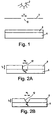
- Figure 1 shows schematically the method for performing lithography on a semiconductor substrate.
- a monochromatic light source 2 is directed towards a mask 4, behind which is situated a substrate 6 coated with a photoactive resist 8.
- a gap 10 of width w is provided in the mask 4 which allows light to reach the resist 8 on the substrate 6.
- the substrate 6 may typically be of silicon, or silicon oxide, or silicon nitride.
- the light is turned on for a predetermined period of time, which causes chemical changes in the resist 8.
- the aim of the process is that the location of these chemical changes should exactly mirror the pattern provided by gaps 10 in the mask 4.
- the exposed layer is removed using a chemical developer.
- the combination of exposure to light with developing will be referred to as "removal" of resist.
- FIG 2A shows the ideal profile of a slot 12 formed by removal of resist 8 from a substrate 6.
- the width w b at the bottom of the slot 12 is equal to the width w t at the top of the slot 12, and this in turn is equal to the width w of the gap 10 in the mask 4 (see Figure 1).
- the exposure to light required to ensure that w b ⁇ w is known as the exposure to size (E S ). This is the exposure needed to define a feature at its target size.
- FIG. 2B shows the profile of the same slot 12 at an earlier stage of the process.
- the exposure has been sufficient to clear the resist 8 just enough to reach the substrate 6.
- w t may have reached w
- w b is only just non-zero.
- This exposure is termed the exposure to clear (E C ), and is the exposure needed to just clear a critical feature at high resolution.
- E C exposure to clear
- E O The exposure to just clear an "open field" area, i.e. an area without any critical patterns and thus one which would not be affected by diminishing aerial image intensity as the pattern size approaches the imaging wavelength, is expressed as E O .
- the metric commonly used in the set-up of photoresist processes in integrated circuit (IC) manufacturing is the ratio E S / E O .
- the margin for error in the determination of the exposure to be used depends on the difference between the exposure required to exactly define a feature at the interface between the resist 8 and the substrate 6, and the exposure needed to just clear to the interface. Ideally, this difference should be as large as possible so that a small variation in exposure will not adversely affect the definition of the features.
- a safe margin typically quoted for E S / E O is 1.4.
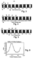
- Figure 3 shows the simulated pictorial representation of a "swing curve" for resist 14 on silicon.
- the figure shows the profile 16, 18 of a slot 12 defined through the thickness of the resist 14, at eight different resist thicknesses varying from 0.98 ⁇ m to 1.12 ⁇ m. Shading in the figure can be disregarded. It can be seen that the slot width is greatest for a resist thickness of 0.96 ⁇ m, then diminishes as the resist thickness increases, so that the minimum slot width occurs at a resist thickness of 1.06 ⁇ m; as the resist thickness continues to inrease the slot width increases again up to a second maximum for a resist thickness of 1.12.
- the resist profile 16, 18 exhibits a small undercut 20 at the resist / silicon interface 24.
- the ratio E S / E C is substantially unaffected by resist thickness changes and varies between 1.095 and 1.105 through a "swing curve" cycle.
- Figure 4 shows the simulated pictorial representation of a "swing curve" for resist 14 on silicon nitride.
- the figure shows the profile 16, 18 of a slot 12 defined through the thickness of the resist 14, for eight different nitride thicknesses varying from 0.1 ⁇ m to 0.2 ⁇ m. This time the resist thickness has been kept constant. Shading in the figure can again be disregarded.
- Figure 4 shows that for a constant resist thickness the nitride "swing curve” results in the resist profile 16, 18 either being undercut 20 or exhibiting a "foot” 22.
- the "foot” 22 on the resist profile 16, 18 is not desirable as it may be transferred into the etched feature and adversely affect field oxide growth.
- Figure 5 shows a "swing curve" for resist 14 on silicon nitride.
- the figure shows the profile 16, 18 of a slot 12 defined through the thickness of the resist 14, for eight different resist thicknesses varying from 0.1 ⁇ m to 0.2 ⁇ m, for a constant nitride thickness. Shading in the figure can again be disregarded. Although the width of the slot 12 varies with resist 14 thickness, the profile 16, 18 at the edge of the slot 12 does not. In other words, in Figure 5 all of the profiles 16, 18 exhibit a "foot" 22.
- nitride thickness will vary depending on the specification of its deposition process, while the resist thickness has to be determined from a wide range of process integration factors.
- the value of E S / E C therefore needs to be added to the process optimisation parameters to protect against the risk of resist scumming during development.
- the resist thickness to be used in conjunction with the target nitride thickness is normally chosen, whenever possible, such that the process operating point is insensitive to nitride thickness changes, at a "swing curve" turning point, which will also be a turning point of the E S / E C function. So care must be taken to choose resist thickness at or near the turning point of the nitride "swing curve" which corresponds to minimum reflectivity (maximum incoupling of energy) which is also a maximum of E S / E C .
- the invention is not limited to the use of light at around 365nm. Other wavelengths may be used, for example 248nm and 193nm.
Landscapes
- Physics & Mathematics (AREA)
- General Physics & Mathematics (AREA)
- Exposure Of Semiconductors, Excluding Electron Or Ion Beam Exposure (AREA)
- Exposure And Positioning Against Photoresist Photosensitive Materials (AREA)
Applications Claiming Priority (2)
| Application Number | Priority Date | Filing Date | Title |
|---|---|---|---|
| GB9916730 | 1999-07-16 | ||
| GBGB9916730.6A GB9916730D0 (en) | 1999-07-16 | 1999-07-16 | Integrated circuit manufacture |
Publications (2)
| Publication Number | Publication Date |
|---|---|
| EP1069478A2 true EP1069478A2 (de) | 2001-01-17 |
| EP1069478A3 EP1069478A3 (de) | 2003-03-26 |
Family
ID=10857379
Family Applications (1)
| Application Number | Title | Priority Date | Filing Date |
|---|---|---|---|
| EP00305618A Withdrawn EP1069478A3 (de) | 1999-07-16 | 2000-07-04 | Resistbehandlung in der Herstellung von integrierten Schaltkreisen |
Country Status (3)
| Country | Link |
|---|---|
| US (1) | US6531264B1 (de) |
| EP (1) | EP1069478A3 (de) |
| GB (1) | GB9916730D0 (de) |
Families Citing this family (1)
| Publication number | Priority date | Publication date | Assignee | Title |
|---|---|---|---|---|
| EP1819313B1 (de) * | 2004-11-16 | 2010-12-29 | 3M Innovative Properties Company | Dentalfüllstoffe und zusammensetzungen mit phosphatsalzen |
Family Cites Families (5)
| Publication number | Priority date | Publication date | Assignee | Title |
|---|---|---|---|---|
| JPS61285716A (ja) | 1985-06-12 | 1986-12-16 | Hitachi Ltd | レジスト塗布方法 |
| US4891094A (en) * | 1989-05-25 | 1990-01-02 | Motorola, Inc. | Method of optimizing photoresist contrast |
| US5476738A (en) | 1994-05-12 | 1995-12-19 | International Business Machines Corporation | Photolithographic dose determination by diffraction of latent image grating |
| US6025116A (en) * | 1997-03-31 | 2000-02-15 | Siemens Aktiengesellschaft | Etching of contact holes |
| US5916717A (en) | 1998-03-19 | 1999-06-29 | Industrial Technology Research Institute | Process utilizing relationship between reflectivity and resist thickness for inhibition of side effect caused by halftone phase shift masks |
-
1999
- 1999-07-16 GB GBGB9916730.6A patent/GB9916730D0/en not_active Ceased
-
2000
- 2000-07-04 EP EP00305618A patent/EP1069478A3/de not_active Withdrawn
- 2000-07-14 US US09/616,342 patent/US6531264B1/en not_active Expired - Lifetime
Also Published As
| Publication number | Publication date |
|---|---|
| EP1069478A3 (de) | 2003-03-26 |
| GB9916730D0 (en) | 1999-09-15 |
| US6531264B1 (en) | 2003-03-11 |
Similar Documents
| Publication | Publication Date | Title |
|---|---|---|
| US7811746B2 (en) | Method of patterning a positive tone resist layer overlaying a lithographic substrate | |
| JP4482543B2 (ja) | リソグラフィ基板の露光方法 | |
| US5354632A (en) | Lithography using a phase-shifting reticle with reduced transmittance | |
| WO2002023272A1 (en) | Dual layer reticle blank and manufacturing process | |
| US7713682B2 (en) | Substrate, method of exposing a substrate, machine readable medium | |
| US7358111B2 (en) | Imageable bottom anti-reflective coating for high resolution lithography | |
| EP1478978B1 (de) | Selbstausrichtende strukturausbildung unter verwendung zweier wellenlängen | |
| JP4613364B2 (ja) | レジストパタン形成方法 | |
| US20090219496A1 (en) | Methods of Double Patterning, Photo Sensitive Layer Stack for Double Patterning and System for Double Patterning | |
| KR20030002145A (ko) | 반도체소자의 패턴 형성 방법 | |
| GB2135793A (en) | Bilevel ultraviolet resist system for patterning substrates of high reflectivity | |
| US6093507A (en) | Simplified process for fabricating levinson and chromeless type phase shifting masks | |
| EP1069478A2 (de) | Resistbehandlung in der Herstellung von integrierten Schaltkreisen | |
| US5543252A (en) | Method for manufacturing exposure mask and the exposure mask | |
| GB2244349A (en) | Method for manufacturing a mask | |
| KR100272518B1 (ko) | 감광막 패터닝방법 | |
| JP3036500B2 (ja) | フォトレジストパターン形成方法及び半導体基板 | |
| KR100586531B1 (ko) | 패턴 밀도에 따른 패턴 식각 시간 설정 방법 | |
| KR100688710B1 (ko) | 반사 방지막 식각 방법 | |
| KR100549272B1 (ko) | 미세선폭을 갖는 반도체 소자의 제조 방법 | |
| KR100476378B1 (ko) | 탑표면이미지프로세스에의해형성된레지스트패턴제거방법 | |
| De Beeck et al. | STRATEGIES TO IMPROVE LINEWIDTH CONTROL FOR 0.25 μm AND 0.18 μm DEVICES | |
| Tritchkov et al. | Proximity effects correction for advanced optical lithography processes | |
| Beeck et al. | Strategies to Improve Linewidth Control for 0.25. MU. m and 0.18. MU. m devices. | |
| Himel et al. | Microfabrication of controlled angle diffusers used for resolution enhancement in microlithography |
Legal Events
| Date | Code | Title | Description |
|---|---|---|---|
| PUAI | Public reference made under article 153(3) epc to a published international application that has entered the european phase |
Free format text: ORIGINAL CODE: 0009012 |
|
| AK | Designated contracting states |
Kind code of ref document: A2 Designated state(s): AT BE CH CY DE DK ES FI FR GB GR IE IT LI LU MC NL PT SE |
|
| AX | Request for extension of the european patent |
Free format text: AL;LT;LV;MK;RO;SI |
|
| PUAL | Search report despatched |
Free format text: ORIGINAL CODE: 0009013 |
|
| AK | Designated contracting states |
Kind code of ref document: A3 Designated state(s): AT BE CH CY DE DK ES FI FR GB GR IE IT LI LU MC NL PT SE Designated state(s): AT BE CH CY DE DK ES FI FR GB GR IE IT LI LU MC NL PT SE |
|
| AX | Request for extension of the european patent |
Extension state: AL LT LV MK RO SI |
|
| RAP1 | Party data changed (applicant data changed or rights of an application transferred) |
Owner name: ZARLINK SEMICONDUCTOR LIMITED |
|
| 17P | Request for examination filed |
Effective date: 20030923 |
|
| AKX | Designation fees paid |
Designated state(s): AT BE CH CY DE DK ES FI FR GB GR IE IT LI LU MC NL PT SE |
|
| RAP1 | Party data changed (applicant data changed or rights of an application transferred) |
Owner name: X-FAB SEMICONDUCTOR FOUNDRIES AG |
|
| 17Q | First examination report despatched |
Effective date: 20090114 |
|
| STAA | Information on the status of an ep patent application or granted ep patent |
Free format text: STATUS: THE APPLICATION IS DEEMED TO BE WITHDRAWN |
|
| 18D | Application deemed to be withdrawn |
Effective date: 20090526 |