EP1069461B1 - Liquid crystal display with wide viewing angle range - Google Patents
Liquid crystal display with wide viewing angle range Download PDFInfo
- Publication number
- EP1069461B1 EP1069461B1 EP00113712A EP00113712A EP1069461B1 EP 1069461 B1 EP1069461 B1 EP 1069461B1 EP 00113712 A EP00113712 A EP 00113712A EP 00113712 A EP00113712 A EP 00113712A EP 1069461 B1 EP1069461 B1 EP 1069461B1
- Authority
- EP
- European Patent Office
- Prior art keywords
- liquid crystal
- film
- retardation film
- retardation
- polarizer
- Prior art date
- Legal status (The legal status is an assumption and is not a legal conclusion. Google has not performed a legal analysis and makes no representation as to the accuracy of the status listed.)
- Expired - Lifetime
Links
Images


Classifications
-
- G—PHYSICS
- G02—OPTICS
- G02F—OPTICAL DEVICES OR ARRANGEMENTS FOR THE CONTROL OF LIGHT BY MODIFICATION OF THE OPTICAL PROPERTIES OF THE MEDIA OF THE ELEMENTS INVOLVED THEREIN; NON-LINEAR OPTICS; FREQUENCY-CHANGING OF LIGHT; OPTICAL LOGIC ELEMENTS; OPTICAL ANALOGUE/DIGITAL CONVERTERS
- G02F1/00—Devices or arrangements for the control of the intensity, colour, phase, polarisation or direction of light arriving from an independent light source, e.g. switching, gating or modulating; Non-linear optics
- G02F1/01—Devices or arrangements for the control of the intensity, colour, phase, polarisation or direction of light arriving from an independent light source, e.g. switching, gating or modulating; Non-linear optics for the control of the intensity, phase, polarisation or colour
- G02F1/13—Devices or arrangements for the control of the intensity, colour, phase, polarisation or direction of light arriving from an independent light source, e.g. switching, gating or modulating; Non-linear optics for the control of the intensity, phase, polarisation or colour based on liquid crystals, e.g. single liquid crystal display cells
- G02F1/133—Constructional arrangements; Operation of liquid crystal cells; Circuit arrangements
- G02F1/1333—Constructional arrangements; Manufacturing methods
- G02F1/1335—Structural association of cells with optical devices, e.g. polarisers or reflectors
- G02F1/13363—Birefringent elements, e.g. for optical compensation
- G02F1/133632—Birefringent elements, e.g. for optical compensation with refractive index ellipsoid inclined relative to the LC-layer surface
-
- G—PHYSICS
- G02—OPTICS
- G02F—OPTICAL DEVICES OR ARRANGEMENTS FOR THE CONTROL OF LIGHT BY MODIFICATION OF THE OPTICAL PROPERTIES OF THE MEDIA OF THE ELEMENTS INVOLVED THEREIN; NON-LINEAR OPTICS; FREQUENCY-CHANGING OF LIGHT; OPTICAL LOGIC ELEMENTS; OPTICAL ANALOGUE/DIGITAL CONVERTERS
- G02F1/00—Devices or arrangements for the control of the intensity, colour, phase, polarisation or direction of light arriving from an independent light source, e.g. switching, gating or modulating; Non-linear optics
- G02F1/01—Devices or arrangements for the control of the intensity, colour, phase, polarisation or direction of light arriving from an independent light source, e.g. switching, gating or modulating; Non-linear optics for the control of the intensity, phase, polarisation or colour
- G02F1/13—Devices or arrangements for the control of the intensity, colour, phase, polarisation or direction of light arriving from an independent light source, e.g. switching, gating or modulating; Non-linear optics for the control of the intensity, phase, polarisation or colour based on liquid crystals, e.g. single liquid crystal display cells
- G02F1/133—Constructional arrangements; Operation of liquid crystal cells; Circuit arrangements
- G02F1/1333—Constructional arrangements; Manufacturing methods
- G02F1/1335—Structural association of cells with optical devices, e.g. polarisers or reflectors
- G02F1/13363—Birefringent elements, e.g. for optical compensation
- G02F1/133634—Birefringent elements, e.g. for optical compensation the refractive index Nz perpendicular to the element surface being different from in-plane refractive indices Nx and Ny, e.g. biaxial or with normal optical axis
-
- G—PHYSICS
- G02—OPTICS
- G02F—OPTICAL DEVICES OR ARRANGEMENTS FOR THE CONTROL OF LIGHT BY MODIFICATION OF THE OPTICAL PROPERTIES OF THE MEDIA OF THE ELEMENTS INVOLVED THEREIN; NON-LINEAR OPTICS; FREQUENCY-CHANGING OF LIGHT; OPTICAL LOGIC ELEMENTS; OPTICAL ANALOGUE/DIGITAL CONVERTERS
- G02F2413/00—Indexing scheme related to G02F1/13363, i.e. to birefringent elements, e.g. for optical compensation, characterised by the number, position, orientation or value of the compensation plates
- G02F2413/10—Indexing scheme related to G02F1/13363, i.e. to birefringent elements, e.g. for optical compensation, characterised by the number, position, orientation or value of the compensation plates with refractive index ellipsoid inclined, or tilted, relative to the LC-layer surface O plate
- G02F2413/105—Indexing scheme related to G02F1/13363, i.e. to birefringent elements, e.g. for optical compensation, characterised by the number, position, orientation or value of the compensation plates with refractive index ellipsoid inclined, or tilted, relative to the LC-layer surface O plate with varying inclination in thickness direction, e.g. hybrid oriented discotic LC
Definitions
- the present invention relates to a liquid crystal display having a wide viewing angle range.
- Conventional liquid crystal displays generally use TN (Twisted Nematic) or STN (Super Twisted Nematic) type apparatuses.
- TN Transmission Nematic
- STN Super Twisted Nematic
- Each of these liquid crystal displays comprises a liquid crystal cell having a liquid crystal layer in which liquid crystal molecules are twisted at a predetermined twist angle between a pair of transparent substrates on the front and rear sides, each of which has a transparent electrode on its inner surface, and front and rear polarizers sandwiching the liquid crystal cell.
- the TN- or STN-type liquid crystal display has a narrow observation angle range, i.e., viewing angle in which display with satisfactory contrast can be observed.
- the observation angle range i.e., viewing angle in which display with satisfactory contrast can be observed becomes narrow, and the display suffers color tinge.
- the liquid crystal display of the first aspect of the present invention when a voltage is applied to the electrodes sandwiching the liquid crystal layer, residual retardation generated due to the influence of liquid crystal molecules which are not sufficiently aligned in the application direction near the front and rear substrates of the liquid crystal layer is compensated by the first and second retardation films, and the retardation difference that changes depending on the incident angle when light that has passed through one of the polarizers passes through the liquid crystal layer is compensated by the third retardation film.
- the liquid crystal display of the present invention can realize bright display and dark display within a wide viewing angle range and can also realize display with high contrast as the ratio of the maximum transmittance to the minimum transmittance.
- each of the first and second retardation films comprises a discotic liquid crystal layer in which liquid crystal molecules are aligned to gradually rise from an aligned state along one surface, from one surface toward the other surface of the first or second retardation film, and has the axial direction, in which the refractive index is minimized, in a direction along an average molecular axis direction of discotic liquid crystal molecules in an intermediate direction in a direction of thickness of the discotic liquid crystal layer, and the direction component of the axial direction in the film plane of each of the first and second retardation films is set parallel to the direction of the aligning treatment of the corresponding adjacent substrate.
- the discotic liquid crystal layers of the first and second retardation films can compensate residual retardation due to the liquid crystal molecules near the front and rear substrates.
- the liquid crystal cell in which the direction of aligning treatment of the alignment film formed on the front substrate is perpendicular to that of the alignment film formed on the rear substrate has the twisted liquid crystal layer sandwiched by the substrate, the pair of polarizers have the absorption axes parallel to the direction of aligning treatment of the alignment films formed on the adjacent substrates of the liquid crystal cell; and the third retardation film/films has/have the direction in which the refractive index in the film plane is maximized in substantially parallel to the absorption axis of the adjacent polarizer.
- the retardation difference due to the difference in incident angle is compensated by the third retardation film/films, so the transmittance does not change depending on the incident angle.
- the first retardation film compensates residual retardation due to the alignment of liquid crystal molecules near the front substrate
- the second retardation film compensates residual retardation due to the alignment of liquid crystal molecules near the rear substrate.
- retardation of light that becomes incident on the liquid crystal layer obliquely with respect to the normal direction to the liquid crystal cell is different from that of light incident in the normal direction.
- this retardation difference is almost canceled by refractive index anisotropy in the film plane of the third retardation film when the light passes through the film, the retardation difference generated when the light passes through the liquid crystal layer can be compensated.
- the light that has passed through the rear polarizer is polarized to oscillate in a direction almost parallel to the absorption axis of the front polarizer, so the light is absorbed.
- the light is polarized to oscillate in a direction perpendicular to the absorption axis of the front polarizer, so the light can pass through the front polarizer.
- the first and second retardation films compensate residual retardation in liquid crystal molecules aligned along the substrate surfaces near the substrates, excluding the intermediate portion of the liquid crystal layer, where the liquid crystal molecules are aligned in the application direction.
- Light incident from one of the polarizers passes through the first and second retardation films while remaining the linearly polarized and is absorbed by the absorption axis of the other polarizer, so the display becomes dark.
- the liquid crystal display of the present invention since the retardation difference in the liquid crystal layer due to the difference in incident angle to the liquid crystal cell or residual retardation generated by the liquid crystal molecules in the part of the liquid crystal layer near the substrates when a voltage is applied is compensated, a change in transmittance due to the difference in incident angle to the liquid crystal cell is minimum.
- the transmittance can be satisfactorily controlled by controlling the voltage to be applied to the liquid crystal layer, the contrast as the ratio of the maximum transmittance to the minimum transmittance can be improved within a wide viewing angle range.
- the third retardation film/films is/are preferably inserted in a position between the front polarizer and the first retardation film or/and a position between the rear polarizer and the second retardation film.
- an s-axis represents the direction in which the refractive index is maximized in the film plane
- an f-axis represents a direction perpendicular to the s-axis in the film plane
- a z-axis represents a normal direction to the film plane
- ns be a refractive index along the s-axis
- nf be a refractive index along the f-axis
- nz be a refractive index along the z-axis
- the refractive indices preferably satisfy 0 ⁇ (ns - nz)/(ns - nf) ⁇ 1.
- a value of a product ⁇ nd of a birefringence index and liquid crystal layer thickness d of the liquid crystal cell falls within a range of 300 to 500 nm, and letting d' be a thickness of each third retardation film, each third retardation film has retardation with which a value (ns - nf) ⁇ d' falls within a range of 250 to 450 nm, and a value (ns - nz) ⁇ d' falls within a range of 70 to 450 nm.
- Each third retardation film may be laid out such that the direction in which the refractive index in the film plane is maximized is substantially perpendicular to the absorption axis of the adjacent polarizer.
- Liquid crystal display devices will be described below as embodiments of the present invention with reference to the accompanying drawing.
- FIGS. 1 to 15 show the first embodiment of the present invention.
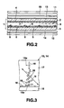
- FIG. 1 is an exploded perspective view of a liquid crystal display.
- FIG. 2 is a sectional view showing part of the liquid crystal display.
- the liquid crystal display of this embodiment has a liquid crystal cell 1, and front and rear polarizers 11 and 12 sandwiching the liquid crystal cell 1.
- a first retardation film 13 is inserted between the liquid crystal cell 1 and the front polarizer 11.
- a second retardation film 14 is inserted between the liquid crystal cell 1 and the rear polarizer 12.
- a third retardation film 19 is inserted between the first retardation film 13 and the adjacent front polarizer 11.
- a nematic liquid crystal layer 9 is formed between a pair of transparent substrates 2 and 3 on the front and rear sides, which are jointed via a frame-like sealing material (not shown), so as to be present in a region enclosed by the sealing material.
- the pair of substrates 2 and 3 have transparent electrodes 4 and 5 on their inner surfaces, respectively.
- the liquid crystal cell 1 used in this embodiment employs the active matrix scheme.
- the electrode 5 formed on the inner surface of the rear substrate (lower substrate in FIG. 2) 3 comprises a plurality of pixel electrodes arrayed in the row and column directions to form a matrix.
- the electrode 4 formed on the inner surface of the front substrate 2 is a film-like counter electrode opposing the plurality of pixel electrodes 5.
- a plurality of TFTs (thin-film transistors) 6 are formed on the inner surface of the rear substrate 3 in correspondence with the plurality of pixel electrodes 5, respectively.
- FIG. 2 schematically illustrates each TFT 6, it comprises a gate electrode formed on the substrate 3, a transparent gate insulating film formed on almost the entire surface of the substrate 3 so as to cover the gate electrode, an i-type semiconductor film formed on the gate insulating film and opposing the gate electrode, and source and drain electrodes formed on both side portions of the I-type semiconductor film via an n-type semiconductor film.
- the pair of substrates 2 and 3 have, on their inner surfaces, alignment films 7 and 8 covering the electrodes 4 and 5, respectively. The alignment films 7 and 8 are aligned by rubbing their film planes in predetermined directions.
- the liquid crystal display of this embodiment is a TN-type liquid crystal display.
- the alignment directions near the substrates 2 and 3 are regulated by aligning the alignment films 7 and 8 formed on the inner surfaces of the pair of substrates 2 and 3.
- the liquid crystal molecules are twisted at a twist angle of about 90° between the substrates 2 and 3.
- the front polarizer 11 and rear polarizer 12 are arranged having their absorption axes 11a and 12a (FIG. 1) almost perpendicular to each other.
- the first and second retardation films 13 and 14 inserted between the liquid crystal cell 1 and the front polarizer 11 and between the liquid crystal cell 1 and the rear polarizer 12, respectively, have negative optical anisotropy with which the refractive index is minimized in a direction tilted in a predetermined direction with respect to the normal line to the film plane.
- FIG. 3 is a schematic sectional view of the first and second retardation films 13 and 14.
- Each of the first and second retardation films 13 and 14 used in this embodiment is formed from a discotic liquid crystal layer 17 in which discotic liquid crystal molecules 18 aligned along the film plane are hybrid-aligned to gradually rise from one surface toward the other surface.
- Each of the first and second retardation films 13 and 14, each of which comprises the discotic liquid crystal layer 17, is manufactured by the following method: an aligning treatment film 16 for tilting the discotic liquid crystal molecules 18 in one direction at a uniform pretilt angle is formed on a transparent base film 15 by obliquely depositing SiO (silicon oxide), for example, a photo-setting discotic polymer liquid crystal is applied to the surface of the aligning treatment film 16 to a predetermined thickness, then, an electric or magnetic field is applied from the upper surface side to hybrid-align the tilted discotic liquid crystal molecules 18 to make them gradually rise from the upper surface toward the liquid crystal layer surface of the base film 15, and in this state, the discotic polymer liquid crystal is hardened by light irradiation.
- SiO silicon oxide
- the first and second retardation films 13 and 14 have negative optical anisotropy along the tilt direction of the hybrid-aligned discotic liquid crystal molecules 18.
- the refractive index is minimized in a direction along an average molecular axis 18a of the discotic liquid crystal molecules 18 in the intermediate layer of the discotic liquid crystal layer 17 and toward the surface (surface on the base film 15 side) on which the discotic liquid crystal molecules 18 are tilt-aligned, i.e., a direction N indicated by an arrow in FIG. 3.
- the direction N in which the refractive index is minimized will be referred to as the axial direction of the first or second retardation film.
- the first and second retardation films 13 and 14 are inserted between the liquid crystal cell 1 and the front polarizer 11 and between the liquid crystal cell 1 and the rear polarizer 12, respectively, having, in predetermined directions, their axial directions N in which the refractive indices are minimized.
- the third retardation film 19 has an s-axis along which the refractive index is maximized in the film plane, an f-axis perpendicular to the s-axis in the film plane, and a z-axis along the normal line to the film plane.
- ns, nf, and nz be the refractive indices along the respective axes.
- the third retardation film 19 is inserted between the first retardation film 13 and the adjacent front polarizer 11 having, in a predetermined direction, the s-axis direction in which the refractive index is maximized in the film plane.
- FIG. 1 shows the layout of the elements of the liquid crystal display according to this embodiment, and the layout directions of the elements.
- the liquid crystal cell 1 is laid out such that an aligning treatment direction 2a of the front substrate 2 is shifted by about 45° counterclockwise with respect to an abscissa x of the screen, which is indicated by an alternate long and short dashed line, when viewed from the front side, while an aligning treatment direction 3a of the rear substrate 3 is shifted by about 45° clockwise with respect to the abscissa x when viewed from the front side.
- the liquid crystal molecules in the liquid crystal layer 9 of the liquid crystal cell 1 are twisted counterclockwise at almost 90° from the rear substrate 3 toward the front substrate 2, when viewed from the front side, as indicated by a broken arrow in FIG. 1.
- the first retardation film 13 is laid out such that the direction component along the film plane in the axial direction N, in which the refractive index is minimized, is shifted by about 45° counterclockwise with respect to the abscissa x when viewed from the front side.
- the second retardation film 14 is laid out such that the direction component along the film plane in the axial direction N, in which the refractive index is minimized, is shifted by about 45° clockwise with respect to the abscissa x when viewed from the front side.
- the direction component of the first retardation film 13 along the film plane in the axial direction N, in which the refractive index is minimized, and the aligning treatment direction 2a of the front substrate 2 are almost parallel to each other in opposite directions.
- the direction component of the second retardation film 14 along the film plane in the axial direction N, in which the refractive index is minimized, and the aligning treatment direction 3a of the rear substrate 3 are almost parallel to each other in opposite directions.
- the surface opposing the liquid crystal cell 1 may be either the surface on the base film 15 side, on which the discotic liquid crystal molecules 18 are aligned along the film plane, or the surface on which the discotic liquid crystal molecules 18 are raised with respect to the surface of the base film 15.
- the front polarizer 11 is laid out such that the absorption axis 11a is shifted by about 45° counterclockwise with respect to the abscissa x when viewed from the front side so as to be almost parallel to the aligning treatment direction 2a of the front substrate 2.
- the rear polarizer 12 is laid out such that the absorption axis 12a is shifted by about 45° clockwise with respect to the abscissa x when viewed from the front side so as to be almost parallel to the aligning treatment direction 3a of the rear substrate 3.
- the absorption axes 11a and 12a of the front and rear polarizers 11 and 12 are perpendicular to each other.
- the third retardation film 19 is laid out such that the direction (s-axis) in which the refractive index is maximized in the film plane is shifted by about 45° counterclockwise or clockwise (counterclockwise in FIG. 1) with respect to the abscissa x when viewed from the front side.
- the s-axis of the third retardation film 19 is almost parallel to the absorption axis 11a of the front polarizer 11 adjacent to the third retardation film 19 and also parallel or perpendicular to the aligning treatment direction 2a of the front substrate 2.
- the refractive indices ns, nf, and nz in the directions of s-, f-, and z-axes of the third retardation film 19 have a following relationship. 0 ⁇ (ns - nz)/(ns - nf) ⁇ 1
- the refractive index anisotropy (ns - nf) in the film plane is equal to or larger than the refractive index anisotropy (ns - nz) in the direction of film thickness.
- the third retardation film 19 has retardation corresponding to a product ⁇ nd of a birefringence index ⁇ n and thickness d of the liquid crystal layer 9 of the liquid crystal cell 1.
- a value (ns - nf)d' falls within the range of 250 to 450 nm
- a value (ns - nz)d' falls within the range of 70 to 450 nm.
- the liquid crystal display having the above arrangement can obtain high-contrast display at a wide viewing angle because the first and second retardation films 13 and 14 having negative optical anisotropy with which the refractive index is minimized in the axial direction N tilted in a predetermined direction with respect to the normal line to the film plane are inserted between the liquid crystal cell 1 and the front polarizer 11 and between the liquid crystal cell 1 and the rear polarizer 12, respectively, such that the axial direction N in which the refractive index is minimized is directed in a predetermined direction, and the third retardation film 19 is inserted between the first retardation film 13 and the adjacent front polarizer 11.
- the first and second retardation films 13 and 14 are inserted between the liquid crystal cell 1 and the front and rear polarizers 11 and 12, respectively, such that the direction components along the film planes in the axial directions N, in which the refractive indices are minimized, are set along the aligning treatment directions 2a and 3a of the substrates 2 and 3, respectively.
- the third retardation film 19 is inserted between the front polarizer 11 and the first retardation film 13 such that the direction (s-axis) which has refractive index anisotropy in the film plane and in which the refractive index in the film plane is maximized becomes parallel to the absorption axis 11a of the front polarizer 11.
- the retardation difference generated by the difference in incident angle of light that becomes incident obliquely with respect to the normal direction to the liquid crystal display and passes through the liquid crystal layer 9, and residual retardation generated in the liquid crystal molecules near the substrates 2 and 3 of the liquid crystal layer 9 when a voltage is applied to the electrodes 5 and 6 sandwiching the liquid crystal layer 9 can be compensated.
- Light incident from the normal direction to the liquid crystal display passes through the rear polarizer 12.
- the light passes through the second retardation film 14 while oscillating in a direction perpendicular to the direction component along the film plane in the axial direction N in which the refractive index is minimized.
- the light also passes through the liquid crystal layer 9 with twist alignment while changing the oscillation direction by almost 90°.
- the oscillation direction is perpendicular to the aligning treatment direction 2a of the front substrate 2.
- the light passes through the first retardation film 13 while oscillating in a direction perpendicular to the direction component along the film plane in the axial direction N in which the refractive index is minimized, and emerges from the first retardation film 13.
- the polarized light becomes incident on the third retardation film 19 almost perpendicularly to the s-axis parallel to the aligning treatment direction 2a.
- the light in the linearly polarized state passes through the third retardation film 19 without changing the oscillation direction.
- the light finally passes through the front polarizer 11 having the absorption axis 11a parallel to the s-axis and emerges from the liquid crystal display.
- the light incident on the liquid crystal display from the normal direction becomes polarized light that propagates through the portion between the second retardation film 14 and the first retardation film 13 without changing its oscillation direction perpendicular to the absorption axis 12a of the rear polarizer 12.
- the polarized light becomes incident on the third retardation film, whose s-axis is arranged parallel to the aligning treatment direction 2a, almost perpendicularly to the s-axis.
- the polarized light in the linear polarized state passes through the third retardation film without changing the oscillation direction, i.e., with an oscillation component perpendicular to the absorption axis 12a of the rear polarizer 12.
- the polarized light is absorbed by the absorption axis 11a of the front polarizer 11, which is perpendicular to the absorption axis 12a of the rear polarizer 12.
- the difference between retardation generated in obliquely passing through the liquid crystal layer 9 and that in passing in the normal direction is compensated by the third retardation film 19.
- the light incident on the second retardation film 14 can emerge from the third retardation film 19 with almost no change in oscillation direction and is absorbed by the absorption axis 11a of the front polarizer 11, which is perpendicular to the absorption axis 12a of the rear polarizer 12.
- the first and second retardation films 13 and 14 are formed by aligning the discotic liquid crystal molecules 18, the refractive index anisotropy of the component perpendicular to the film plane direction is small. For this reason, the first and second retardation films 13 and 14 can compensate only residual retardation generated near the substrates 2 and 3 of the liquid crystal layer 9 without generating any retardation to compensate the retardation generated in accordance with the incident angle when the light obliquely passes through the liquid crystal layer 9.
- the retardation difference due to the difference in incident angle can be compensated independently of whether the s-axis of the third retardation film 19 is set parallel or perpendicular to the absorption axis 11a of the front polarizer 11 and the aligning treatment direction 2a.
- the retardation difference due to the difference in incident angle of light is compensated by the refractive index anisotropy (ns - nf) of the film plane.
- the refractive indices ns, nf, and nz in the directions of s-, f-, and z-axes have the following relationship. 0 ⁇ (ns - nz)/(ns - nf) ⁇ 1
- the refractive index anisotropy (ns - nf) in the film plane is equal to or larger than the refractive index anisotropy (ns - nz) of the section in the direction of film thickness, light incident in a direction neither parallel nor perpendicular to the s-axis can be elliptically polarized. For this reason, the retardation difference can be compensated by the third retardation film 19, and the viewing angle range can be made sufficiently wide.
- a third retardation film 19 having retardation with which the value (ns - nf)d' falls within the range of 250 to 450 nm, and the value (ns - nz)d' falls within the range of 70 to 450 nm is preferably used.
- the viewing angle range can be made sufficiently wide, and high-contrast display with satisfactory color appearance and almost no stripe colors can be obtained.
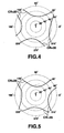
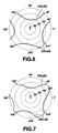
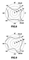
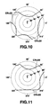
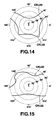
- FIGS. 4 to 15 are views showing measurement data of the viewing angle range of the liquid crystal display of this embodiment.
- FIG. 16 is a view showing the measurement data of the viewing angle range of a liquid crystal display as a comparative example having no third retardation film. These figures show the viewing angle ranges in which display with contrast CR of 20 or more can be observed.
- a plurality of concentric circles indicated by broken lines represent observation angles of 20°, 40°, 60°, and 80° with respect to the normal line (0°) to the screen of the liquid crystal display.
- Angles at the outer periphery represent the display observation directions, in which 0° indicates the right of the screen in the horizontal direction, 90° indicates the upper side of the screen in the vertical direction, 180° indicates the left of the screen in the horizontal direction, and 270° indicates the lower side of the screen in the vertical direction.
- the characteristics of the third retardation film 19, the layout directions of the third retardation film 19 with respect to the absorption axis 11a of the front polarizer 11, and the viewing angle ranges are as follows.
- the viewing angle ranges in Mode 1 are 40° (upper) to 50° (lower), and 46° (left) to 50° (right).
- the viewing angle ranges in Mode 2 are 30° (upper) to 50° (lower), and 50° (left) to 50° (right).
- the viewing angle ranges in Mode 3 are 36° (upper) to 58° (lower), and 60° (left) to 50° (right).
- the viewing angle ranges in Mode 4 are 40° (upper) to 50° (lower), and 80° (left) to 50° (right).
- the viewing angle ranges in Mode 5 are 30° (upper) to 54° (lower), and 52° (left) to 46° (right).
- the viewing angle ranges in Mode 6 are 45° (upper) to 45° (lower), and 80° (left) to 60° (right).
- the viewing angle ranges in Mode 7 are 38° (upper) to 60° (lower), and 80° (left) to 54° (right).
- the viewing angle ranges in Mode 8 are 38° (upper) to 60° (lower), and 80° (left) to 58° (right).
- the viewing angle ranges in Mode 9 are 30° (upper) to 50° (lower), and 50° (left) to 50° (right).
- the viewing angle ranges in Mode 10 are 58° (upper) to 36° (lower), and 65° (left) to 80° (right).
- the viewing angle ranges in Mode 11 are 28° (upper) to 38° (lower), and 48° (left) to 44° (right).
- the viewing angle ranges in Mode 12 are 56° (upper) to 34° (lower), and 70° (left) to 80° (right).
- the vertical and horizontal viewing angle ranges of the screen in which the contrast CR of 20 or more can be obtained are 40° (upper) to 40° (lower), and 44° (left) to 46° (right), as shown in FIG. 16.
- the horizontal viewing angles of the screens are wider as compared to the comparative apparatus.
- a liquid crystal display is mainly required to have a wide horizontal viewing angle.
- liquid crystal display of this embodiment a liquid crystal display in which the aligning treatment directions 2a and 3a of the front and rear substrates 2 and 3 of the liquid crystal cell 1 are shifted by about 45° with respect to the abscissa x of the screen, and the liquid crystal molecules in the liquid crystal cell 1 are twisted at a twist angle of about 90° between the substrates 2 and 3.
- the absorption axis 11a of the front polarizer 11 is almost parallel to the aligning treatment direction 2a
- the absorption axis 12a of the rear polarizer 12 is almost parallel to the aligning treatment direction 3a
- the third retardation film 19 is laid out such that the direction (s-axis) which has refractive index anisotropy in the film plane and in which the refractive index in the film plane is maximized becomes almost parallel or perpendicular to the absorption axis 11a of the adjacent front polarizer 11, the refractive indices ns, nf, and nz in the directions of s-, f-, and z-axes of the third retardation film 19 have the relationship 0 ⁇ (ns - nz)/(ns - nf) ⁇ 1, the value ⁇ nd of the liquid crystal cell 1 falls within
- the viewing angle range tends to be wide when the s-axis is set perpendicular to the absorption axis 11a of the front polarizer 11.
- Modes 1 to 12 The viewing angle characteristics in Modes 1 to 12 will be compared. Especially, in Mode 3 shown in FIG. 6, Mode 4 shown in FIG. 7, Mode 6 shown in FIG. 9, Mode 7 shown in FIG. 10, Mode 8 shown in FIG. 11, Mode 10 shown in FIG. 13, and Mode 12 shown in FIG. 15, the horizontal viewing angle is wider than that of the comparative apparatus having no third retardation film 19, and the vertical viewing angle is also sufficiently wide. For the horizontal viewing angle, the characteristics shown in FIG. 11 (Mode 8), FIG. 13 (Mode 10), and FIG. 15 (Mode 12) are excellent. Especially, the characteristic shown in FIG. 13 (Mode 10) is most satisfactory.
- preferable modes are Modes 3, 4, 6, 7, 8, 10, and 12. More preferable modes are Modes 8, 10, and 12. A much more preferable mode is Mode 10.
- Modes 3, 4, 6, 7, 8, 10, and 12 will be applied to the characteristics of the third retardation film 19.
- the liquid crystal cell 1 used in the above embodiment employs the active matrix scheme.
- the liquid crystal cell 1 may employ a simple matrix scheme in which a plurality of scan electrodes along the row direction are formed on the inner surface of one of the pair of substrates 2 and 3, and a plurality of signal electrodes along the column direction are formed on the inner surface of the other substrate.
- the liquid crystal cell 1 may display either a monochrome image or a multi-color image by using color filters of a plurality of colors, for example, three colors (red, green, and blue) in correspondence with the plurality of pixel regions.
- the liquid crystal display of the above embodiment is a TN-type liquid crystal display in which the liquid crystal molecules of the liquid crystal cell 1 are aligned at a twist angle of about 90°.
- the present invention can also be applied to, e.g., an STN-type liquid crystal display in which liquid crystal molecules are aligned at a twist angle of 180° to 270° (normally 220° to 250°), or homogeneous liquid crystal display.
- the first and second retardation films are inserted between the liquid crystal cell and the rear and front polarizers, the axial directions are set along the aligning treatment directions of the substrates, and the third retardation film 19 whose refractive indices along the s-, f-, and z-axes have the relationship ns > nz ⁇ nf is inserted between at least one of the first and second retardation film and the adjacent polarizer whereby the residual retardation generated near the substrates in the liquid crystal layer and the retardation difference generated in the liquid crystal layer by the difference in incident angle when light becomes obliquely incident can be compensated.
- FIG. 17 is an exploded perspective view showing a liquid crystal display according to the second embodiment of the present invention.
- a third retardation film 19' is inserted between a second retardation film 14 and an adjacent rear polarizer 12.
- This liquid crystal display is different from that of the first embodiment only in the insertion position of the third retardation film 19'.
- the same reference numerals as in the first embodiment denote the same parts in the second embodiment, and a detailed description thereof will be omitted.
- aligning treatment directions 2a and 3a of front substrate 2 and rear substrate 3 of a liquid crystal cell 1 the twist angle of liquid crystal molecules, axial directions N in which the refractive indices of first retardation film 13 and second retardation film 14 are minimized, and the directions of absorption axes 11a and 12a of front polarizer 11 and rear polarizer 12 are the same as in the first embodiment.
- the third retardation film 19' inserted between the second retardation film 14 and the rear polarizer 12 has a direction which has refractive index anisotropy in the film plane and in which the refractive index in the film plane is maximized.
- the direction in which the refractive index in the film plane is maximized is set almost parallel or perpendicular to the absorption axis 12a of the adjacent rear polarizer 12.
- refractive indices ns, nf, and nz of the s-axis along which the refractive index in the film plane is maximized have a relationship ns > nz ⁇ nf, and preferably, 0 ⁇ (ns - nz)/(ns - nf) ⁇ 1.
- the first and second retardation films 13 and 14 are arranged on the front and rear sides of the liquid crystal cell 1, respectively.
- the front polarizer 11 and rear polarizer 12 are arranged outside the first and second retardation films 13 and 14.
- the third retardation film 19' is inserted between the second retardation film 14 and the rear polarizer 12.
- Incoming light on this liquid crystal display passes through the rear polarizer 12. Then, polarized light oscillating in a direction perpendicular to the absorption axis of the polarizer 12 enters the third retardation film 19' at an angle corresponding to the s-axis along which the refractive index in the film plane is maximized and the incident angle with respect to the normal line to the liquid crystal display.
- the oscillation direction of the polarized light is perpendicular to the s-axis, so the light passes through the third retardation film without changing the oscillation direction.
- the residual retardation due to the liquid crystal molecules near the substrates 2 and 3 of the liquid crystal layer 9 is compensated by the first and second retardation films 13 and 14.
- the light that has passed through the rear polarizer 12 oscillates in a direction parallel to the absorption axis 11a of the front polarizer 11 and therefore is absorbed by the absorption axis 11a. For this reason, black display with low transmittance can be obtained.
- display with high transmittance can be obtained independently of the incident angle of light when no voltage is applied to the electrodes sandwiching the liquid crystal layer, and display with low transmittance can be obtained when a voltage is applied to the electrodes sandwiching the liquid crystal layer, so high-contrast display can be realized in a wide viewing angle range.
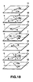
- FIG. 18 is an exploded perspective view showing a liquid crystal display according to the third embodiment of the present invention.
- third retardation films 19 and 19' are respectively inserted between a first retardation film 13 and a front polarizer 11 and between a second retardation film 14 and a rear polarizer 12.
- This liquid crystal display is different from that of the first embodiment only in the insertion position of the third retardation film 19'.
- the same reference numerals as in the first embodiment denote the same parts in the third embodiment, and a detailed description thereof will be omitted.
- aligning treatment directions 2a and 3a of front substrate 2 and rear substrate 3 of a liquid crystal cell 1 the twist angle of liquid crystal molecules, axial directions N in which the refractive indices of the first retardation film 13 and second retardation film 14 are minimized, and the directions of absorption axes 11a and 12a of front polarizer 11 and rear polarizer 12 are the same as in the first embodiment.
- the third retardation film 19 inserted between the first retardation film 13 and the front polarizer 11 is arranged such that the direction which has refractive index anisotropy in the film plane and in which the refractive index in the film plane is maximized is set almost parallel or perpendicular to the absorption axis 11a of the adjacent front polarizer 11.
- the third retardation film 19' inserted between the second retardation film 14 and the rear polarizer 12 is arranged such that the direction which has refractive index anisotropy in the film plane and in which the refractive index in the film plane is maximized is set almost parallel or perpendicular to the absorption axis 12a of the adjacent rear polarizer 12.
- refractive indices ns, nf, and nz of the s-axis along which the refractive index in the film plane is maximized have a relationship ns > nz ⁇ nf, and preferably, 0 ⁇ (ns - nz)/(ns - nf) ⁇ 1.
- the first and second retardation films 13 and 14 are arranged on the front and rear sides of the liquid crystal cell 1, respectively.
- the front polarizer 11 and rear polarizer 12 are arranged outside the first and second retardation films 13 and 14.
- the third retardation film 19 is inserted between the first retardation film 13 and the front polarizer 11.
- the third retardation film 19' is inserted between the second retardation film 14 and the rear polarizer 12.
- the refractive indices in the ns, nf, and nz-axis directions and film thickness d' of each of the third retardation films 19 and 19' are set such that the retardation difference generated in correspondence with the incident angle from the normal direction to the liquid crystal display when light passes through the liquid crystal layer 9 is compensated by the retardation difference generated when the light passes through a corresponding one of the third retardation films 19 and 19' located in front and rear sides of the liquid crystal cell 1.
- a retardation difference generated in correspondence with the incident angle with respect to the normal direction when light passes through the liquid crystal layer 9 is compensated by the retardation difference generated when the light passes through the third retardation film 19' obliquely with respect to the normal direction and that generated by the elliptically polarized light when the light passes through the third retardation film 19 arranged on the front side of the liquid crystal cell 1, as described for the liquid crystal display of the first embodiment.
- display with high transmittance can be obtained independently of the incident angle of light when no voltage is applied to the electrodes 5 and 6 sandwiching the liquid crystal layer 9, and display with low transmittance can be obtained when a voltage is applied to the electrodes 5 and 6 sandwiching the liquid crystal layer 9, so high-contrast display can be realized in a wide viewing angle range.
Landscapes
- Physics & Mathematics (AREA)
- Nonlinear Science (AREA)
- Mathematical Physics (AREA)
- Chemical & Material Sciences (AREA)
- Crystallography & Structural Chemistry (AREA)
- General Physics & Mathematics (AREA)
- Optics & Photonics (AREA)
- Liquid Crystal (AREA)
- Devices For Indicating Variable Information By Combining Individual Elements (AREA)
- Polarising Elements (AREA)
Applications Claiming Priority (2)
| Application Number | Priority Date | Filing Date | Title |
|---|---|---|---|
| JP18597499 | 1999-06-30 | ||
| JP18597499A JP4032568B2 (ja) | 1999-06-30 | 1999-06-30 | 液晶表示装置 |
Publications (3)
| Publication Number | Publication Date |
|---|---|
| EP1069461A2 EP1069461A2 (en) | 2001-01-17 |
| EP1069461A3 EP1069461A3 (en) | 2003-01-22 |
| EP1069461B1 true EP1069461B1 (en) | 2004-03-03 |
Family
ID=16180145
Family Applications (1)
| Application Number | Title | Priority Date | Filing Date |
|---|---|---|---|
| EP00113712A Expired - Lifetime EP1069461B1 (en) | 1999-06-30 | 2000-06-28 | Liquid crystal display with wide viewing angle range |
Country Status (8)
| Country | Link |
|---|---|
| US (1) | US6307608B1 (ja) |
| EP (1) | EP1069461B1 (ja) |
| JP (1) | JP4032568B2 (ja) |
| KR (1) | KR100335662B1 (ja) |
| CN (1) | CN1161644C (ja) |
| DE (1) | DE60008643T2 (ja) |
| HK (1) | HK1034320A1 (ja) |
| TW (1) | TWI282459B (ja) |
Cited By (1)
| Publication number | Priority date | Publication date | Assignee | Title |
|---|---|---|---|---|
| CN101762905B (zh) * | 2007-01-26 | 2012-09-12 | 卡西欧计算机株式会社 | 液晶显示元件 |
Families Citing this family (39)
| Publication number | Priority date | Publication date | Assignee | Title |
|---|---|---|---|---|
| EP1130452A4 (en) * | 1999-09-09 | 2007-10-17 | Citizen Holdings Co Ltd | LIQUID CRYSTAL SHUTTER |
| JP4566384B2 (ja) | 2000-10-30 | 2010-10-20 | 日東電工株式会社 | 偏光板 |
| JP4566385B2 (ja) * | 2000-10-30 | 2010-10-20 | 日東電工株式会社 | 偏光板 |
| JP2002148434A (ja) | 2000-11-08 | 2002-05-22 | Nitto Denko Corp | 偏光板 |
| JP5067684B2 (ja) * | 2001-06-14 | 2012-11-07 | Nltテクノロジー株式会社 | 液晶表示装置及びその製造方法 |
| JP4328205B2 (ja) * | 2001-10-04 | 2009-09-09 | 富士フイルム株式会社 | 透過型液晶表示装置 |
| JP3863446B2 (ja) * | 2002-03-08 | 2006-12-27 | シャープ株式会社 | 液晶表示装置 |
| TWI225551B (en) * | 2002-04-18 | 2004-12-21 | Nitto Denko Corp | Polarization plate having optical compensation function and liquid crystal display device using the same |
| US6995823B1 (en) * | 2002-07-30 | 2006-02-07 | Rockwell Collins, Inc. | Viewing angle for liquid crystal display system and method |
| DE60321481D1 (de) * | 2002-11-02 | 2008-07-17 | Merck Patent Gmbh | Optisch kompensiertes elektrooptisches lichtmodula |
| US6891589B2 (en) | 2002-12-16 | 2005-05-10 | Nitto Denko Corporation | Optical film, elliptically polarizing plate and image display |
| JP3807375B2 (ja) * | 2003-02-06 | 2006-08-09 | セイコーエプソン株式会社 | 液晶表示装置および電子機器 |
| JP4564795B2 (ja) * | 2003-09-30 | 2010-10-20 | 株式会社日立製作所 | 液晶表示装置 |
| KR100677050B1 (ko) * | 2003-10-22 | 2007-01-31 | 주식회사 엘지화학 | +a-플레이트와 +c-플레이트를 이용한 시야각보상필름을 포함하는 면상 스위칭 액정 표시장치 |
| CN1299129C (zh) * | 2003-11-13 | 2007-02-07 | 力特光电科技股份有限公司 | 防窥装置及其制造方法 |
| KR20050051400A (ko) * | 2003-11-27 | 2005-06-01 | 삼성전자주식회사 | 액정 표시 패널 및 이를 갖는 액정 표시 장치 |
| JP4382502B2 (ja) | 2004-01-05 | 2009-12-16 | Nec液晶テクノロジー株式会社 | 液晶表示装置 |
| JP2005201960A (ja) | 2004-01-13 | 2005-07-28 | Seiko Epson Corp | 液晶装置および投射型表示装置 |
| JP4046116B2 (ja) * | 2004-02-26 | 2008-02-13 | セイコーエプソン株式会社 | 液晶装置および電子機器 |
| KR100682230B1 (ko) | 2004-11-12 | 2007-02-12 | 주식회사 엘지화학 | 수직 배향 액정표시장치 |
| KR100789512B1 (ko) * | 2005-06-01 | 2007-12-28 | 도시바 마쯔시따 디스플레이 테크놀로지 컴퍼니, 리미티드 | 액정 표시 소자 |
| CA2616376A1 (en) * | 2005-07-25 | 2007-02-01 | Duke University | Methods, systems, and computer program products for optimization of probes for spectroscopic measurement in turbid media |
| US7511792B2 (en) | 2005-07-29 | 2009-03-31 | Lg Chem, Ltd. | In-plane switching liquid crystal display having simple structure |
| EP1826604B1 (en) * | 2006-01-31 | 2015-12-23 | Semiconductor Energy Laboratory Co., Ltd. | Display device |
| JP2007218940A (ja) * | 2006-02-14 | 2007-08-30 | Epson Imaging Devices Corp | 液晶装置及び電子機器 |
| EP1826606B1 (en) * | 2006-02-24 | 2012-12-26 | Semiconductor Energy Laboratory Co., Ltd. | Display device |
| KR100741127B1 (ko) | 2006-06-02 | 2007-07-19 | 삼성에스디아이 주식회사 | 액정 디스플레이 소자 |
| KR101476841B1 (ko) * | 2006-12-28 | 2014-12-24 | 엘지디스플레이 주식회사 | 시야각 제어 액정표시장치 |
| JP4311492B2 (ja) * | 2007-01-26 | 2009-08-12 | カシオ計算機株式会社 | 液晶表示素子及び放送受信装置 |
| WO2009054167A1 (ja) * | 2007-10-26 | 2009-04-30 | Sharp Kabushiki Kaisha | 複合位相差板、およびそれを備えた光学補償偏光板並びに液晶表示装置 |
| US20110090433A1 (en) * | 2008-07-02 | 2011-04-21 | Kazuyoshi Sakuragi | Liquid crystal display device |
| JP5581782B2 (ja) * | 2009-04-17 | 2014-09-03 | ソニー株式会社 | 撮像装置 |
| JP5544844B2 (ja) * | 2009-11-27 | 2014-07-09 | カシオ計算機株式会社 | 液晶表示素子 |
| CN108845451B (zh) * | 2012-07-30 | 2021-12-10 | 东洋纺株式会社 | 液晶显示装置、偏光板和偏振片保护膜 |
| CN105510999B (zh) * | 2016-01-28 | 2019-05-28 | 京东方科技集团股份有限公司 | 减反射结构及其制造方法、显示器及其制造方法 |
| TW201921060A (zh) * | 2017-09-15 | 2019-06-01 | 美商瑞爾D斯帕克有限責任公司 | 用於可切換定向顯示器的光學堆疊結構 |
| CN109696757A (zh) * | 2017-10-23 | 2019-04-30 | 中强光电股份有限公司 | 偏光式视角控制元件、偏光式视角控制显示装置以及偏光式视角控制光源模块 |
| JP6873203B2 (ja) * | 2018-09-19 | 2021-05-19 | シャープ株式会社 | 反射型液晶表示装置 |
| CN110490184B (zh) * | 2019-08-23 | 2022-09-09 | 京东方科技集团股份有限公司 | 一种纹路识别装置及其纹路识别方法 |
Family Cites Families (16)
| Publication number | Priority date | Publication date | Assignee | Title |
|---|---|---|---|---|
| EP0367616A3 (en) * | 1988-11-04 | 1991-04-24 | Matsushita Electric Industrial Co., Ltd. | Optical liquid crystal element |
| JPH04194820A (ja) * | 1990-11-22 | 1992-07-14 | Sharp Corp | 液晶表示装置 |
| JPH0580326A (ja) * | 1991-09-20 | 1993-04-02 | Ricoh Co Ltd | 液晶表示素子 |
| JPH07301794A (ja) * | 1994-04-28 | 1995-11-14 | Casio Comput Co Ltd | 液晶表示装置 |
| US5638200A (en) * | 1995-02-03 | 1997-06-10 | Ois Optical Imaging Systems, Inc. | Liquid crystal display with tilted retardation film |
| JPH0915586A (ja) * | 1995-06-29 | 1997-01-17 | Nec Corp | 液晶表示装置 |
| JPH0968706A (ja) * | 1995-09-01 | 1997-03-11 | Ricoh Co Ltd | 液晶表示素子 |
| US6208396B1 (en) * | 1996-10-25 | 2001-03-27 | Sumitomo Chemical Company, Limited | Normally white mode twisted nematic liquid crystal display device having improved viewing angle characteristics |
| JP3452742B2 (ja) * | 1996-12-24 | 2003-09-29 | シャープ株式会社 | 液晶表示装置 |
| TW515925B (en) * | 1996-12-25 | 2003-01-01 | Sharp Kk | Liquid crystal display device |
| JP3678540B2 (ja) * | 1997-05-27 | 2005-08-03 | 新日本石油株式会社 | 液晶表示素子 |
| US5990997A (en) * | 1997-06-05 | 1999-11-23 | Ois Optical Imaging Systems, Inc. | NW twisted nematic LCD with negative tilted retarders for improved viewing characteristics |
| US5895106A (en) * | 1997-06-13 | 1999-04-20 | Ois Optical Imaging Systems, Inc. | NW twisted nematic LCD with negative tilted retarders on one side of liquid crystal cell |
| US6064457A (en) * | 1997-12-25 | 2000-05-16 | Fuji Photo Film Co., Ltd. | Liquid crystal display with ellipsoidal polarizing plate having an optically anisotropic layer transparent substrate and a polarizing membrane |
| JPH11212078A (ja) * | 1998-01-22 | 1999-08-06 | Fuji Photo Film Co Ltd | 液晶表示装置 |
| FR2789186B1 (fr) * | 1999-02-02 | 2002-01-18 | Sextant Avionique | Empilement optique elargissant l'angle de vue horizontal d'un ecran a cristaux liquides |
-
1999
- 1999-06-30 JP JP18597499A patent/JP4032568B2/ja not_active Expired - Fee Related
-
2000
- 2000-06-28 DE DE60008643T patent/DE60008643T2/de not_active Expired - Lifetime
- 2000-06-28 EP EP00113712A patent/EP1069461B1/en not_active Expired - Lifetime
- 2000-06-28 US US09/606,055 patent/US6307608B1/en not_active Expired - Lifetime
- 2000-06-29 TW TW089112880A patent/TWI282459B/zh not_active IP Right Cessation
- 2000-06-29 KR KR1020000036323A patent/KR100335662B1/ko not_active IP Right Cessation
- 2000-06-30 CN CNB001269593A patent/CN1161644C/zh not_active Expired - Fee Related
-
2001
- 2001-07-11 HK HK01104808A patent/HK1034320A1/xx not_active IP Right Cessation
Cited By (1)
| Publication number | Priority date | Publication date | Assignee | Title |
|---|---|---|---|---|
| CN101762905B (zh) * | 2007-01-26 | 2012-09-12 | 卡西欧计算机株式会社 | 液晶显示元件 |
Also Published As
| Publication number | Publication date |
|---|---|
| DE60008643T2 (de) | 2004-08-05 |
| US6307608B1 (en) | 2001-10-23 |
| EP1069461A3 (en) | 2003-01-22 |
| HK1034320A1 (en) | 2001-10-19 |
| EP1069461A2 (en) | 2001-01-17 |
| JP4032568B2 (ja) | 2008-01-16 |
| DE60008643D1 (de) | 2004-04-08 |
| CN1161644C (zh) | 2004-08-11 |
| TWI282459B (en) | 2007-06-11 |
| KR100335662B1 (ko) | 2002-05-06 |
| JP2001013501A (ja) | 2001-01-19 |
| KR20010007574A (ko) | 2001-01-26 |
| CN1281157A (zh) | 2001-01-24 |
Similar Documents
| Publication | Publication Date | Title |
|---|---|---|
| EP1069461B1 (en) | Liquid crystal display with wide viewing angle range | |
| US6339460B1 (en) | Liquid crystal display device | |
| JP2982869B2 (ja) | 液晶表示装置 | |
| JP3763401B2 (ja) | 液晶表示装置 | |
| US8638403B2 (en) | Liquid crystal display device | |
| US7440056B2 (en) | Homeotropic alignment type liquid crystal display device | |
| US7643116B2 (en) | Liquid crystal display device | |
| EP1600810B1 (en) | Liquid crystal display device | |
| US8319923B2 (en) | Liquid crystal display device having two discotic liquid crystal compensating films and two retardation films | |
| US20060215096A1 (en) | Liquid crystal display | |
| EP0538796B1 (en) | Homeotropic liquid crystal display device | |
| JP4441971B2 (ja) | 液晶表示素子 | |
| JP3399773B2 (ja) | 液晶表示装置 | |
| US7499127B2 (en) | Liquid crystal display device having red, green and blue filters in which the liquid crystal layer thickness for the red filter portion is equal to the green filter portion but greater than the blue filter portion | |
| US5940155A (en) | Liquid crystal displays containing tilted optical axis compensation films having a negative birefringence | |
| JP3342417B2 (ja) | 液晶表示装置 | |
| JP3399795B2 (ja) | 液晶表示装置 | |
| JPH05313159A (ja) | 液晶表示装置 | |
| US7589811B2 (en) | Liquid crystal display device | |
| TWI344048B (en) | Liquid crystal display device having liquid crystal layer in which liquid crystal molecules are homogeneously oriented | |
| KR100950358B1 (ko) | 액정 디스플레이 디바이스 | |
| JPH06347782A (ja) | 液晶表示装置 | |
| JP2002182184A (ja) | 液晶表示装置 |
Legal Events
| Date | Code | Title | Description |
|---|---|---|---|
| PUAI | Public reference made under article 153(3) epc to a published international application that has entered the european phase |
Free format text: ORIGINAL CODE: 0009012 |
|
| 17P | Request for examination filed |
Effective date: 20000628 |
|
| AK | Designated contracting states |
Kind code of ref document: A2 Designated state(s): AT BE CH CY DE DK ES FI FR GB GR IE IT LI LU MC NL PT SE |
|
| AX | Request for extension of the european patent |
Free format text: AL;LT;LV;MK;RO;SI |
|
| PUAL | Search report despatched |
Free format text: ORIGINAL CODE: 0009013 |
|
| AK | Designated contracting states |
Kind code of ref document: A3 Designated state(s): AT BE CH CY DE DK ES FI FR GB GR IE IT LI LU MC NL PT SE |
|
| AX | Request for extension of the european patent |
Free format text: AL;LT;LV;MK;RO;SI |
|
| AKX | Designation fees paid |
Designated state(s): DE FR GB |
|
| GRAP | Despatch of communication of intention to grant a patent |
Free format text: ORIGINAL CODE: EPIDOSNIGR1 |
|
| GRAS | Grant fee paid |
Free format text: ORIGINAL CODE: EPIDOSNIGR3 |
|
| GRAA | (expected) grant |
Free format text: ORIGINAL CODE: 0009210 |
|
| AK | Designated contracting states |
Kind code of ref document: B1 Designated state(s): DE FR GB |
|
| REG | Reference to a national code |
Ref country code: GB Ref legal event code: FG4D |
|
| REG | Reference to a national code |
Ref country code: IE Ref legal event code: FG4D |
|
| REF | Corresponds to: |
Ref document number: 60008643 Country of ref document: DE Date of ref document: 20040408 Kind code of ref document: P |
|
| ET | Fr: translation filed | ||
| PLBE | No opposition filed within time limit |
Free format text: ORIGINAL CODE: 0009261 |
|
| STAA | Information on the status of an ep patent application or granted ep patent |
Free format text: STATUS: NO OPPOSITION FILED WITHIN TIME LIMIT |
|
| 26N | No opposition filed |
Effective date: 20041206 |
|
| REG | Reference to a national code |
Ref country code: IE Ref legal event code: MM4A |
|
| REG | Reference to a national code |
Ref country code: FR Ref legal event code: PLFP Year of fee payment: 16 |
|
| PGFP | Annual fee paid to national office [announced via postgrant information from national office to epo] |
Ref country code: GB Payment date: 20150618 Year of fee payment: 16 Ref country code: DE Payment date: 20150619 Year of fee payment: 16 |
|
| PGFP | Annual fee paid to national office [announced via postgrant information from national office to epo] |
Ref country code: FR Payment date: 20150619 Year of fee payment: 16 |
|
| REG | Reference to a national code |
Ref country code: DE Ref legal event code: R119 Ref document number: 60008643 Country of ref document: DE |
|
| GBPC | Gb: european patent ceased through non-payment of renewal fee |
Effective date: 20160628 |
|
| REG | Reference to a national code |
Ref country code: FR Ref legal event code: ST Effective date: 20170228 |
|
| PG25 | Lapsed in a contracting state [announced via postgrant information from national office to epo] |
Ref country code: DE Free format text: LAPSE BECAUSE OF NON-PAYMENT OF DUE FEES Effective date: 20170103 Ref country code: FR Free format text: LAPSE BECAUSE OF NON-PAYMENT OF DUE FEES Effective date: 20160630 |
|
| PG25 | Lapsed in a contracting state [announced via postgrant information from national office to epo] |
Ref country code: GB Free format text: LAPSE BECAUSE OF NON-PAYMENT OF DUE FEES Effective date: 20160628 |