EP1069455A1 - Optical device formed on a substrate with thermal isolation regions formed therein - Google Patents
Optical device formed on a substrate with thermal isolation regions formed therein Download PDFInfo
- Publication number
- EP1069455A1 EP1069455A1 EP00305569A EP00305569A EP1069455A1 EP 1069455 A1 EP1069455 A1 EP 1069455A1 EP 00305569 A EP00305569 A EP 00305569A EP 00305569 A EP00305569 A EP 00305569A EP 1069455 A1 EP1069455 A1 EP 1069455A1
- Authority
- EP
- European Patent Office
- Prior art keywords
- porous silicon
- waveguide
- substrate
- optical device
- region
- Prior art date
- Legal status (The legal status is an assumption and is not a legal conclusion. Google has not performed a legal analysis and makes no representation as to the accuracy of the status listed.)
- Granted
Links
- 239000000758 substrate Substances 0.000 title claims abstract description 46
- 230000003287 optical effect Effects 0.000 title claims abstract description 35
- 238000002955 isolation Methods 0.000 title description 2
- 229910021426 porous silicon Inorganic materials 0.000 claims abstract description 54
- XUIMIQQOPSSXEZ-UHFFFAOYSA-N Silicon Chemical compound [Si] XUIMIQQOPSSXEZ-UHFFFAOYSA-N 0.000 claims abstract description 28
- 229910052710 silicon Inorganic materials 0.000 claims abstract description 28
- 239000010703 silicon Substances 0.000 claims abstract description 28
- 238000005253 cladding Methods 0.000 claims description 16
- 238000010438 heat treatment Methods 0.000 abstract description 4
- 239000010410 layer Substances 0.000 description 39
- VYPSYNLAJGMNEJ-UHFFFAOYSA-N Silicium dioxide Chemical compound O=[Si]=O VYPSYNLAJGMNEJ-UHFFFAOYSA-N 0.000 description 24
- 239000000463 material Substances 0.000 description 19
- 230000008859 change Effects 0.000 description 13
- BASFCYQUMIYNBI-UHFFFAOYSA-N platinum Chemical compound [Pt] BASFCYQUMIYNBI-UHFFFAOYSA-N 0.000 description 12
- 238000000034 method Methods 0.000 description 11
- 239000011521 glass Substances 0.000 description 9
- 235000012431 wafers Nutrition 0.000 description 9
- 239000000377 silicon dioxide Substances 0.000 description 8
- 239000010409 thin film Substances 0.000 description 8
- 230000000694 effects Effects 0.000 description 7
- KRHYYFGTRYWZRS-UHFFFAOYSA-N hydrofluoric acid Substances F KRHYYFGTRYWZRS-UHFFFAOYSA-N 0.000 description 7
- 230000008569 process Effects 0.000 description 7
- VYZAMTAEIAYCRO-UHFFFAOYSA-N Chromium Chemical compound [Cr] VYZAMTAEIAYCRO-UHFFFAOYSA-N 0.000 description 6
- 229910052804 chromium Inorganic materials 0.000 description 6
- 239000011651 chromium Substances 0.000 description 6
- 238000004518 low pressure chemical vapour deposition Methods 0.000 description 6
- 229910052697 platinum Inorganic materials 0.000 description 6
- QPJSUIGXIBEQAC-UHFFFAOYSA-N n-(2,4-dichloro-5-propan-2-yloxyphenyl)acetamide Chemical compound CC(C)OC1=CC(NC(C)=O)=C(Cl)C=C1Cl QPJSUIGXIBEQAC-UHFFFAOYSA-N 0.000 description 5
- 239000000243 solution Substances 0.000 description 5
- 238000002048 anodisation reaction Methods 0.000 description 4
- 230000000873 masking effect Effects 0.000 description 4
- OAICVXFJPJFONN-UHFFFAOYSA-N Phosphorus Chemical compound [P] OAICVXFJPJFONN-UHFFFAOYSA-N 0.000 description 3
- 238000013461 design Methods 0.000 description 3
- 238000005530 etching Methods 0.000 description 3
- 229910052751 metal Inorganic materials 0.000 description 3
- 239000002184 metal Substances 0.000 description 3
- 239000013307 optical fiber Substances 0.000 description 3
- 229910052698 phosphorus Inorganic materials 0.000 description 3
- 239000011574 phosphorus Substances 0.000 description 3
- 238000001020 plasma etching Methods 0.000 description 3
- 238000012545 processing Methods 0.000 description 3
- 230000001902 propagating effect Effects 0.000 description 3
- 229910052814 silicon oxide Inorganic materials 0.000 description 3
- BOTDANWDWHJENH-UHFFFAOYSA-N Tetraethyl orthosilicate Chemical compound CCO[Si](OCC)(OCC)OCC BOTDANWDWHJENH-UHFFFAOYSA-N 0.000 description 2
- 238000013459 approach Methods 0.000 description 2
- QVGXLLKOCUKJST-UHFFFAOYSA-N atomic oxygen Chemical compound [O] QVGXLLKOCUKJST-UHFFFAOYSA-N 0.000 description 2
- 238000004891 communication Methods 0.000 description 2
- 239000012792 core layer Substances 0.000 description 2
- 230000007423 decrease Effects 0.000 description 2
- PCHJSUWPFVWCPO-UHFFFAOYSA-N gold Chemical compound [Au] PCHJSUWPFVWCPO-UHFFFAOYSA-N 0.000 description 2
- 229910052737 gold Inorganic materials 0.000 description 2
- 239000010931 gold Substances 0.000 description 2
- 229910052760 oxygen Inorganic materials 0.000 description 2
- 239000001301 oxygen Substances 0.000 description 2
- 239000002243 precursor Substances 0.000 description 2
- 230000005855 radiation Effects 0.000 description 2
- 238000004544 sputter deposition Methods 0.000 description 2
- 239000002470 thermal conductor Substances 0.000 description 2
- ZOXJGFHDIHLPTG-UHFFFAOYSA-N Boron Chemical compound [B] ZOXJGFHDIHLPTG-UHFFFAOYSA-N 0.000 description 1
- BLRPTPMANUNPDV-UHFFFAOYSA-N Silane Chemical compound [SiH4] BLRPTPMANUNPDV-UHFFFAOYSA-N 0.000 description 1
- RTAQQCXQSZGOHL-UHFFFAOYSA-N Titanium Chemical compound [Ti] RTAQQCXQSZGOHL-UHFFFAOYSA-N 0.000 description 1
- 230000004888 barrier function Effects 0.000 description 1
- 230000008901 benefit Effects 0.000 description 1
- 229910052796 boron Inorganic materials 0.000 description 1
- 238000000151 deposition Methods 0.000 description 1
- 239000002019 doping agent Substances 0.000 description 1
- 239000003792 electrolyte Substances 0.000 description 1
- 239000008151 electrolyte solution Substances 0.000 description 1
- 238000005516 engineering process Methods 0.000 description 1
- 238000011067 equilibration Methods 0.000 description 1
- 239000000835 fiber Substances 0.000 description 1
- 239000010408 film Substances 0.000 description 1
- 238000011065 in-situ storage Methods 0.000 description 1
- 230000001939 inductive effect Effects 0.000 description 1
- 238000009413 insulation Methods 0.000 description 1
- 238000004519 manufacturing process Methods 0.000 description 1
- 230000007246 mechanism Effects 0.000 description 1
- 150000002739 metals Chemical class 0.000 description 1
- 239000000203 mixture Substances 0.000 description 1
- 150000004767 nitrides Chemical class 0.000 description 1
- 238000000059 patterning Methods 0.000 description 1
- 230000010363 phase shift Effects 0.000 description 1
- 229920002120 photoresistant polymer Polymers 0.000 description 1
- 229910021420 polycrystalline silicon Inorganic materials 0.000 description 1
- 229920005591 polysilicon Polymers 0.000 description 1
- 230000004044 response Effects 0.000 description 1
- 239000004065 semiconductor Substances 0.000 description 1
- 229910000077 silane Inorganic materials 0.000 description 1
- 239000010936 titanium Substances 0.000 description 1
- 229910052719 titanium Inorganic materials 0.000 description 1
- 238000012546 transfer Methods 0.000 description 1
Images
Classifications
-
- G—PHYSICS
- G02—OPTICS
- G02F—OPTICAL DEVICES OR ARRANGEMENTS FOR THE CONTROL OF LIGHT BY MODIFICATION OF THE OPTICAL PROPERTIES OF THE MEDIA OF THE ELEMENTS INVOLVED THEREIN; NON-LINEAR OPTICS; FREQUENCY-CHANGING OF LIGHT; OPTICAL LOGIC ELEMENTS; OPTICAL ANALOGUE/DIGITAL CONVERTERS
- G02F1/00—Devices or arrangements for the control of the intensity, colour, phase, polarisation or direction of light arriving from an independent light source, e.g. switching, gating or modulating; Non-linear optics
- G02F1/01—Devices or arrangements for the control of the intensity, colour, phase, polarisation or direction of light arriving from an independent light source, e.g. switching, gating or modulating; Non-linear optics for the control of the intensity, phase, polarisation or colour
- G02F1/011—Devices or arrangements for the control of the intensity, colour, phase, polarisation or direction of light arriving from an independent light source, e.g. switching, gating or modulating; Non-linear optics for the control of the intensity, phase, polarisation or colour in optical waveguides, not otherwise provided for in this subclass
-
- G—PHYSICS
- G02—OPTICS
- G02B—OPTICAL ELEMENTS, SYSTEMS OR APPARATUS
- G02B6/00—Light guides; Structural details of arrangements comprising light guides and other optical elements, e.g. couplings
- G02B6/10—Light guides; Structural details of arrangements comprising light guides and other optical elements, e.g. couplings of the optical waveguide type
- G02B6/12—Light guides; Structural details of arrangements comprising light guides and other optical elements, e.g. couplings of the optical waveguide type of the integrated circuit kind
- G02B2006/12035—Materials
- G02B2006/12061—Silicon
-
- G—PHYSICS
- G02—OPTICS
- G02B—OPTICAL ELEMENTS, SYSTEMS OR APPARATUS
- G02B6/00—Light guides; Structural details of arrangements comprising light guides and other optical elements, e.g. couplings
- G02B6/10—Light guides; Structural details of arrangements comprising light guides and other optical elements, e.g. couplings of the optical waveguide type
- G02B6/12—Light guides; Structural details of arrangements comprising light guides and other optical elements, e.g. couplings of the optical waveguide type of the integrated circuit kind
- G02B2006/12166—Manufacturing methods
- G02B2006/12176—Etching
-
- G—PHYSICS
- G02—OPTICS
- G02F—OPTICAL DEVICES OR ARRANGEMENTS FOR THE CONTROL OF LIGHT BY MODIFICATION OF THE OPTICAL PROPERTIES OF THE MEDIA OF THE ELEMENTS INVOLVED THEREIN; NON-LINEAR OPTICS; FREQUENCY-CHANGING OF LIGHT; OPTICAL LOGIC ELEMENTS; OPTICAL ANALOGUE/DIGITAL CONVERTERS
- G02F1/00—Devices or arrangements for the control of the intensity, colour, phase, polarisation or direction of light arriving from an independent light source, e.g. switching, gating or modulating; Non-linear optics
- G02F1/01—Devices or arrangements for the control of the intensity, colour, phase, polarisation or direction of light arriving from an independent light source, e.g. switching, gating or modulating; Non-linear optics for the control of the intensity, phase, polarisation or colour
- G02F1/011—Devices or arrangements for the control of the intensity, colour, phase, polarisation or direction of light arriving from an independent light source, e.g. switching, gating or modulating; Non-linear optics for the control of the intensity, phase, polarisation or colour in optical waveguides, not otherwise provided for in this subclass
- G02F1/0113—Glass-based, e.g. silica-based, optical waveguides
-
- G—PHYSICS
- G02—OPTICS
- G02F—OPTICAL DEVICES OR ARRANGEMENTS FOR THE CONTROL OF LIGHT BY MODIFICATION OF THE OPTICAL PROPERTIES OF THE MEDIA OF THE ELEMENTS INVOLVED THEREIN; NON-LINEAR OPTICS; FREQUENCY-CHANGING OF LIGHT; OPTICAL LOGIC ELEMENTS; OPTICAL ANALOGUE/DIGITAL CONVERTERS
- G02F1/00—Devices or arrangements for the control of the intensity, colour, phase, polarisation or direction of light arriving from an independent light source, e.g. switching, gating or modulating; Non-linear optics
- G02F1/01—Devices or arrangements for the control of the intensity, colour, phase, polarisation or direction of light arriving from an independent light source, e.g. switching, gating or modulating; Non-linear optics for the control of the intensity, phase, polarisation or colour
- G02F1/0147—Devices or arrangements for the control of the intensity, colour, phase, polarisation or direction of light arriving from an independent light source, e.g. switching, gating or modulating; Non-linear optics for the control of the intensity, phase, polarisation or colour based on thermo-optic effects
-
- G—PHYSICS
- G02—OPTICS
- G02F—OPTICAL DEVICES OR ARRANGEMENTS FOR THE CONTROL OF LIGHT BY MODIFICATION OF THE OPTICAL PROPERTIES OF THE MEDIA OF THE ELEMENTS INVOLVED THEREIN; NON-LINEAR OPTICS; FREQUENCY-CHANGING OF LIGHT; OPTICAL LOGIC ELEMENTS; OPTICAL ANALOGUE/DIGITAL CONVERTERS
- G02F2202/00—Materials and properties
- G02F2202/10—Materials and properties semiconductor
- G02F2202/103—Materials and properties semiconductor a-Si
Definitions
- the present invention relates to optical devices, and in particular, optical waveguides that are coupled with heaters.
- Optical fiber communication systems are becoming more prevalent.
- optical fiber communication systems use a wide variety of optical devices for receiving, transmitting, and using optical signals.
- One type of integrated optical device is a silica optical circuit formed on silicon substrates. The basic structure of such device is described in Henry, C.H., et al., "Silica-based optical integrated circuits," IEE Proc.-Optoelectron, Vol. 143, No. 5, pp. 263-280 (1996).
- heaters are used to effect a change in the refractive index of the device.
- the change in refractive index of the device changes the phase of the signal transmitted through the device.
- Using a heater to effect a controlled change in the refractive index of the optical device is a way to effect a controlled change in the phase of the transmitted optical signal.
- Inducing a controlled phase change in an optical signal is useful in a variety of contexts. In some devices a controlled phase change is induced to tune the optical device. In other devices, a controlled phase change is used as a switching mechanism.
- thermo-optic switches include the N x N optical switch and the add/drop multiplexer.
- a thin film heater is formed on the optical device, which is typically a planar waveguide.
- the planar waveguide consists of a first cladding layer formed on a substrate.
- the core is formed on the first cladding layer.
- a second cladding layer is then formed over the core.
- a thin film heater is then formed on the second cladding layer. The thin film heater is used to effect a desired change in the refractive index of the core and claddings for device operation.
- the temperature of the waveguide is increased.
- the waveguide is in intimate contact with the silicon substrate, which is a good thermal conductor. Consequently, unless the silicon substrate is thermally isolated from the waveguide, it is difficult to effect a local change in waveguide temperature and the power consumed by the heater will be high.
- Mach-Zehnder waveguide interference devices have multiple branches or arms that must be independently heated to effect the desired device operation.
- one arm is heated and the other arm is not to produce a desired differential phase change between the signals from each arm.
- silicon is a good thermal conductor, silicon facilitates temperature equilibration between the heated arm and the unheated arm, which is undesirable. Consequently, there have been attempts to thermally isolate the arms of a silicon-based planar Mach-Zehnder device from each other.
- trenches are etched out under the waveguides to thermally isolate the waveguides from the substrate.
- the trenches increase the amount of time for the device to cool and thus the amount of time it takes for the device to switch back to its unswitched state (the switched state being the heated state).
- Another disadvantage of the trench approach is the complexity of manufacturing involved in extra steps.
- the present invention is directed to an optical device in which heat is used to thermally induce a desired change in the refractive index of the device.
- the device is a waveguide that is formed on a region of porous silicon that is formed in a silicon substrate.
- the porous silicon region has a thermal conductivity that is less than the heat conductivity of silicon oxide. Consequently, less heat is conducted from a heated waveguide formed on a porous silicon region that would otherwise be conducted if the heated waveguide were formed on either silicon or silicon oxide.
- the optical device is fabricated by first forming at least one region of porous silicon in a silicon substrate. Expedients for forming regions of porous silicon in a substrate are well known to one skilled in the art. It is advantageous if the porous silicon is formed using an electrolytic process. In the electrolytic process, silicon is anodized in an electrolytic solution. Such a technique is described in Unagmi, T., et al., "An Isolation Technique Using Oxidized Porous Silicon," Semiconductor Technologies , Vol. 8, Chap. 11, pp. 139-154 (OHMSHAT and North Holland Publishing Company 1983) which is hereby incorporated by reference.
- the silicon substrate is anodized selectively to form porous silicon regions therein.
- the substrate is selectively anodized by forming a mask on the silicon substrate prior to anodization.
- the mask has at least one opening therein.
- the underlying silicon substrate surface is exposed through such openings.
- the porosity of the porous silicon region is also largely a matter of design choice.
- the porosity of the material is controlled by the doping level of the substrate (e.g. silicon wafer) and the anodization condition used to form the porous areas.
- Anodization conditions such as an applied voltage and the associated current density as well as the concentration and pH values of the HF solutions are selected to obtain the desired porosity.
- the range of appropriate porosities is mainly determined by two factors: low heat conductivity and mechanical stability.
- the porous silicon must be porous enough to have heat conductivity lower than that of silicon oxide (1.4 W/m K). In this regard, it is advantageous if the porosity is at least about 50 volume percent.
- the porous silicon need only withstand the rigors of subsequent processing. In these embodiments, porosities up to about ninety-five percent are suitable. In other embodiments where the structural demands on the porous silicon are more rigorous, porosities of up to ninety percent are contemplated. This is because thick (i.e. greater than about 5 ⁇ m) porous layers are brittle and do not provide the required support for the optical device formed thereon.
- the dimensions of the porous silicon region are largely a matter of design choice.
- the depth and size of a porous silicon region depends upon the size of the waveguide subsequently formed on the region and the amount of heat generated by the heater on such device. Since the objective is to stem the heat conducted from the heated waveguide into the substrate, the larger the amount of heat generated by the waveguide, the greater the resistance to thermal conductivity that must be provided by the porous silicon region. As previously noted, one way to increase the porous silicon's resistance to thermal conductivity is to increase its porosity. Another way is to increase the distance heat must travel through the porous silicon region (i.e., the thickness of the porous silicon region) to the substrate.
- the optical device is completed.
- Examples of devices that would benefit from being formed on porous silicon include Wavelength Add-Drop (WAD) for Dense Wavelength Division Multiplexing (DWDM) systems, dynamic wavelength equalizers for chromatic equalization in Er-doped fiber amplifier systems; Mach-Zehnder (MZ) based switches, tunable filters, and Y-branch switches.
- WAD Wavelength Add-Drop
- MZ Mach-Zehnder
- the thickness and porosity of the porous silicon region are selected to balance the efficiency of the device (i.e., the amount of heat needed to switch) and the speed of the device. The better the insulation of the element from the silicon substrate (which functions as a heat sink) the longer it takes for the heat to dissipate from the heated portion of the device, and the lower the frequency of the operation.
- the processes used to form the waveguide on the porous silicon region must be compatible with the porous silicon process. This means that the process for forming the claddings and cores of the devices on the porous silicon can not require conditions that would damage the porous silicon region.
- the temperature range in which the claddings and cores are deposited on the porous silicon region cannot include temperatures that will cause the porous layer to disintegrate.
- Forming the cores and claddings on a porous silicon regions using a standard low-pressure chemical vapor deposition (LPCVD) technique does not unacceptably damage the porous silicon.
- the present invention is directed to an optical device that includes a waveguide with a heat-generating element that is formed on a porous silicon region of a silicon substrate.
- the porous silicon restricts the flow of heat from the heated device. Consequently, the rate at which heat flows from the heat-generating element into the silicon substrate is reduced by the porous silicon region. Since heat flows from the heater at a reduced rate than it otherwise would if the waveguide were formed directly on a silicon substrate, the temperature of the waveguide increases at a faster rate than it otherwise would without a commensurate increase in power consumption by the heater.
- a variety of optical devices have a heat-generating element (e.g. a thin film heater), which is used to effect a desired response in the device. Such devices are well known to one skilled in the art and are not described in detail herein.
- Examples of devices that have heaters disposed on top of waveguides include MZ interferometers. In MZ interferometers, heating one arm of the device without heating the other arm produces a phase difference between the optical signals transmitted in the two arms of the device. Heating the arm changes its refractive index. The change in refractive index increases or decreases the phase delay of the propagating light signal in the heated arm.
- MZ interferometers are incorporated into other devices, such as add-drop filters and gain equalizers.
- a built-in MZ is used to pass or switch a channel to another arm.
- the heater controls the phase shift between the signals propagating in the arms of the device and therefore the amount of light propagating in each of them.
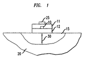
- FIG. 1 illustrates the general structure of a planar waveguide with a thin film heater formed thereon. It consists of three layers: core layer 10; upper clad layer 11; and lower clad 12. In one embodiment, all three layers are silica glass. In alternative embodiments, the layers are plastic. The core layer is doped with phosphorus. The thickness of the individual layers is a matter of design choice. The appropriate thicknesses for a particular application are readily ascertained by one skilled in the art.
- the waveguide is formed on a region of porous silicon 15 formed in a silicon substrate 20.
- the region of porous silicon is formed by depositing a patterned layer of material that defines the desired porous silicon regions by leaving those regions exposed through the mask.
- the mask material is deposited on the substrate and then patterned.
- the masked substrate is then placed in an annodization bath. The portions of the substrate that are exposed to the anodization bath are converted to porous silicon, and the regions covered by the mask are not.
- mask materials are contemplated as suitable.
- suitable mask materials include photoresist, nitride, oxide, and carbide of silicon, polysilicon, and metals that are not soluble in HF solutions (e.g., gold, platinum etc.).
- HF solutions e.g., gold, platinum etc.
- Different masking materials have different etch-resistances for HF and thus should be chosen according to desired etch time and the process complexity.
- a planar waveguide is formed on the porous silicon region.
- a thin film heater 25 is formed on the upper cladding layer 11 of the planar waveguide.
- Silicon wafers doped with a resistivity of 0.01 ⁇ -cm were cleaned and coated with an energy sensitive resist material, Shipley 1822 that was obtained from the Shipley Co. of Marlborough, MA.
- the layer of energy sensitive material was formed on the silicon substrate using standard conditions.
- a pattern was delineated into the energy sensitive material.
- the pattern was a series of lines and spaces wherein the lines had a thickness of 35 ⁇ m and a length of 2.8 mm.
- the lines had a centerline to centerline distance of 175 ⁇ m.
- the pattern was delineated in the energy sensitive resist material using standard lithographic techniques. First, an image was transferred into the energy sensitive material by exposing the resist to patterned radiation. The image was then developed into a pattern by removing the portions of the energy sensitive material that were exposed to radiation. Removing portions of the energy sensitive material exposed the surface of the silicon substrate underlying those portions. The dimensions of the removed portions corresponded to the dimensions of the lines in pattern. In this embodiment the same mask that was used to define the regions of porous silicon was used as the mask to form the heaters on the waveguides.
- the resist was baked at 150°C for 2 minutes. This was done to increase the stability of the resist during subsequent processing.
- the substrate with the patterned masking layer thereon was then subjected to a set of conditions that electrochemically etches silicon.
- the electrochemical cell used here was a standard double-tank cell. A cell of this type is described in Lang, W. et al., Sensors and Actuators A 51, pp. 31-36 (1995).
- the wafer was immersed in HF solution such that that both sides were immersed in solution and the wafer formed a barrier between two half-cells.
- Two platinum electrodes were located in each half-cell on both sides of the wafer. The electrical contact to the backside of the wafer was formed electrolytically, and the corresponding platinum electrode was the anode.
- the platinum electrode in the other half-cell was under cathodic potential.
- the two platinum electrodes were connected to the power supply that drives the current through the wafer.
- the front side of the wafer is anodically etched and porous silicon is formed at the areas not covered with the mask.
- the electrolyte was 35 weight percent ethanoic solution of hydrofluoric acid (HF).
- HF hydrofluoric acid
- a current density of 5 mA/cm 2 provided an etch rate of 0.3 ⁇ m/min and a porosity of about 70%.
- a current density of 40 mA/cm 2 provided an etch rate of 1.4 ⁇ m/min and a porosity of about 80%.
- the substrate was heated to 300°C and held for two hours in an oxygen atmosphere.
- the substrate was then placed in an oxygen-containing atmosphere at 1000°C for one hour.
- the porous silicon was oxidized but did not measurably expand in the vertical direction, i.e., it remained planar with the substrate surface. Because the porous silicon surface did not increase or decrease in elevation compared to the rest of the substrate surface, further processing was not complicated by the presence of the porous silicon region.
- a layer of silica was then deposited on the substrate.
- the silica was deposited using low-pressure chemical vapor deposition (LPCVD).
- LPCVD low-pressure chemical vapor deposition
- a silane precursor was used in the CVD process.
- the silica film had a thickness of about 15 ⁇ m.
- the silica layer was the bottom cladding of the optical device.
- a layer of doped glass material was then deposited on the bottom cladding layer.
- the doped glass was silica doped with phosphorus (seven weight percent).
- the doped glass material was deposited using LPCVD. The dopants were introduced into the glass in situ .
- the core of the optical device was then formed by patterning the doped glass layer.
- An etch mask layer was formed over the doped glass layer.
- the etch mask layer was then patterned, so that the remaining portion of the etch mask layer defined the core of the optical device being formed.
- the doped glass material was then etched using reactive ion etching (RIE). After etching, the portion of the doped glass layer that remains is the core of the optical device. The remaining portion of the RIE etch mask was then removed.
- RIE reactive ion etching
- silica glass is formed over the substrate.
- the layer of silica glass was deposited using LPCVD from tetraethyl orthosilicate (TEOS) precursors.
- TEOS tetraethyl orthosilicate
- the glass composition was silica doped with boron (five weight percent) and phosphorus (2 weight percent).
- a thin film heater was then formed on the upper cladding layer.
- the thin film heater was formed by sputtering a layer of chromium on the upper cladding layer.
- the chromium layer had a thickness of the 200 nm.
- the heaters were defined lithographically in the chromium layer.
- a layer of energy sensitive resist material was formed on the chromium layer and patterned using conventional materials and expedients. The patterned resist material was then used as an etch mask to transfer the pattern into the underlying chromium layer.
- the substrate was selectively etched to remove the silica glass between the individual waveguides. This is accomplished by masking the substrate and selectively etching the silica glass between the waveguides. The steps of masking and etching are conventional and not discussed in detail herein.
- a metal contact was then formed on the heater.
- the metal contact was formed in about the middle of the heater by sputtering, sequentially, layers of titanium (100 nm), platinum (200 nm) and gold (500 nm) on the previously described structure. The layers were then patterned to form the electrically contacts for the chromium heaters previously formed on the substrate.
Landscapes
- Physics & Mathematics (AREA)
- Nonlinear Science (AREA)
- General Physics & Mathematics (AREA)
- Optics & Photonics (AREA)
- Optical Integrated Circuits (AREA)
- Optical Modulation, Optical Deflection, Nonlinear Optics, Optical Demodulation, Optical Logic Elements (AREA)
Abstract
Description
- The present invention relates to optical devices, and in particular, optical waveguides that are coupled with heaters.
- Optical fiber communication systems are becoming more prevalent. In addition to the optical fiber itself, optical fiber communication systems use a wide variety of optical devices for receiving, transmitting, and using optical signals. One type of integrated optical device is a silica optical circuit formed on silicon substrates. The basic structure of such device is described in Henry, C.H., et al., "Silica-based optical integrated circuits," IEE Proc.-Optoelectron, Vol. 143, No. 5, pp. 263-280 (1996).
- In certain optical devices such as thermo-optic switches, heaters are used to effect a change in the refractive index of the device. The change in refractive index of the device changes the phase of the signal transmitted through the device. Using a heater to effect a controlled change in the refractive index of the optical device is a way to effect a controlled change in the phase of the transmitted optical signal. Inducing a controlled phase change in an optical signal is useful in a variety of contexts. In some devices a controlled phase change is induced to tune the optical device. In other devices, a controlled phase change is used as a switching mechanism.
- Examples of thermo-optic switches include the N x N optical switch and the add/drop multiplexer. In thermo-optic switches, a thin film heater is formed on the optical device, which is typically a planar waveguide. The planar waveguide consists of a first cladding layer formed on a substrate. The core is formed on the first cladding layer. A second cladding layer is then formed over the core. A thin film heater is then formed on the second cladding layer. The thin film heater is used to effect a desired change in the refractive index of the core and claddings for device operation.
- To produce the desired phase change in the device, the temperature of the waveguide is increased. However, the waveguide is in intimate contact with the silicon substrate, which is a good thermal conductor. Consequently, unless the silicon substrate is thermally isolated from the waveguide, it is difficult to effect a local change in waveguide temperature and the power consumed by the heater will be high.
- Many devices, such as Mach-Zehnder waveguide interference devices, have multiple branches or arms that must be independently heated to effect the desired device operation. For example, in the two-arm Mach-Zehnder devices, one arm is heated and the other arm is not to produce a desired differential phase change between the signals from each arm. Since silicon is a good thermal conductor, silicon facilitates temperature equilibration between the heated arm and the unheated arm, which is undesirable. Consequently, there have been attempts to thermally isolate the arms of a silicon-based planar Mach-Zehnder device from each other.
- In one approach, trenches are etched out under the waveguides to thermally isolate the waveguides from the substrate. However, the trenches increase the amount of time for the device to cool and thus the amount of time it takes for the device to switch back to its unswitched state (the switched state being the heated state). Another disadvantage of the trench approach is the complexity of manufacturing involved in extra steps.
- Accordingly, ways to control the heat flow from a heated waveguide that is conducted by the substrate are sought.
- The present invention is directed to an optical device in which heat is used to thermally induce a desired change in the refractive index of the device. The device is a waveguide that is formed on a region of porous silicon that is formed in a silicon substrate. The porous silicon region has a thermal conductivity that is less than the heat conductivity of silicon oxide. Consequently, less heat is conducted from a heated waveguide formed on a porous silicon region that would otherwise be conducted if the heated waveguide were formed on either silicon or silicon oxide.
- The optical device is fabricated by first forming at least one region of porous silicon in a silicon substrate. Expedients for forming regions of porous silicon in a substrate are well known to one skilled in the art. It is advantageous if the porous silicon is formed using an electrolytic process. In the electrolytic process, silicon is anodized in an electrolytic solution. Such a technique is described in Unagmi, T., et al., "An Isolation Technique Using Oxidized Porous Silicon," Semiconductor Technologies, Vol. 8, Chap. 11, pp. 139-154 (OHMSHAT and North Holland Publishing Company 1983) which is hereby incorporated by reference.
- The silicon substrate is anodized selectively to form porous silicon regions therein. The substrate is selectively anodized by forming a mask on the silicon substrate prior to anodization. The mask has at least one opening therein. The underlying silicon substrate surface is exposed through such openings.
- Similarly the porosity of the porous silicon region is also largely a matter of design choice. The porosity of the material is controlled by the doping level of the substrate (e.g. silicon wafer) and the anodization condition used to form the porous areas. Anodization conditions such as an applied voltage and the associated current density as well as the concentration and pH values of the HF solutions are selected to obtain the desired porosity. The range of appropriate porosities is mainly determined by two factors: low heat conductivity and mechanical stability. The porous silicon must be porous enough to have heat conductivity lower than that of silicon oxide (1.4 W/m K). In this regard, it is advantageous if the porosity is at least about 50 volume percent. In principle, the higher the porosity is, the lower is the heat conductivity (G. Gesele, G, et al., J. Phys. D: Appl. Phys., Vol. 30, pp. 2911-2916 (1997). Therefore, higher porosity is advantageous because it provides lower heat conductivity. In certain embodiments, the porous silicon need only withstand the rigors of subsequent processing. In these embodiments, porosities up to about ninety-five percent are suitable. In other embodiments where the structural demands on the porous silicon are more rigorous, porosities of up to ninety percent are contemplated. This is because thick (i.e. greater than about 5 µm) porous layers are brittle and do not provide the required support for the optical device formed thereon.
- The dimensions of the porous silicon region are largely a matter of design choice. The depth and size of a porous silicon region depends upon the size of the waveguide subsequently formed on the region and the amount of heat generated by the heater on such device. Since the objective is to stem the heat conducted from the heated waveguide into the substrate, the larger the amount of heat generated by the waveguide, the greater the resistance to thermal conductivity that must be provided by the porous silicon region. As previously noted, one way to increase the porous silicon's resistance to thermal conductivity is to increase its porosity. Another way is to increase the distance heat must travel through the porous silicon region (i.e., the thickness of the porous silicon region) to the substrate.
- After the porous silicon region is formed on the substrate, the optical device is completed. Examples of devices that would benefit from being formed on porous silicon include Wavelength Add-Drop (WAD) for Dense Wavelength Division Multiplexing (DWDM) systems, dynamic wavelength equalizers for chromatic equalization in Er-doped fiber amplifier systems; Mach-Zehnder (MZ) based switches, tunable filters, and Y-branch switches. The thickness and porosity of the porous silicon region are selected to balance the efficiency of the device (i.e., the amount of heat needed to switch) and the speed of the device. The better the insulation of the element from the silicon substrate (which functions as a heat sink) the longer it takes for the heat to dissipate from the heated portion of the device, and the lower the frequency of the operation.
- Furthermore, the processes used to form the waveguide on the porous silicon region must be compatible with the porous silicon process. This means that the process for forming the claddings and cores of the devices on the porous silicon can not require conditions that would damage the porous silicon region. For examples, the temperature range in which the claddings and cores are deposited on the porous silicon region cannot include temperatures that will cause the porous layer to disintegrate. Forming the cores and claddings on a porous silicon regions using a standard low-pressure chemical vapor deposition (LPCVD) technique does not unacceptably damage the porous silicon.
-
- FIG. 1 illustrates an example of an optical device formed on a region of porous silicon.
-
- The present invention is directed to an optical device that includes a waveguide with a heat-generating element that is formed on a porous silicon region of a silicon substrate. The porous silicon restricts the flow of heat from the heated device. Consequently, the rate at which heat flows from the heat-generating element into the silicon substrate is reduced by the porous silicon region. Since heat flows from the heater at a reduced rate than it otherwise would if the waveguide were formed directly on a silicon substrate, the temperature of the waveguide increases at a faster rate than it otherwise would without a commensurate increase in power consumption by the heater.
- A variety of optical devices have a heat-generating element (e.g. a thin film heater), which is used to effect a desired response in the device. Such devices are well known to one skilled in the art and are not described in detail herein. Examples of devices that have heaters disposed on top of waveguides include MZ interferometers. In MZ interferometers, heating one arm of the device without heating the other arm produces a phase difference between the optical signals transmitted in the two arms of the device. Heating the arm changes its refractive index. The change in refractive index increases or decreases the phase delay of the propagating light signal in the heated arm. MZ interferometers are incorporated into other devices, such as add-drop filters and gain equalizers. In an add-drop filter, a built-in MZ is used to pass or switch a channel to another arm. In a gain equalizer, the heater controls the phase shift between the signals propagating in the arms of the device and therefore the amount of light propagating in each of them.
- FIG. 1 illustrates the general structure of a planar waveguide with a thin film heater formed thereon. It consists of three layers:
core layer 10; upper cladlayer 11; and lower clad 12. In one embodiment, all three layers are silica glass. In alternative embodiments, the layers are plastic. The core layer is doped with phosphorus. The thickness of the individual layers is a matter of design choice. The appropriate thicknesses for a particular application are readily ascertained by one skilled in the art. - The waveguide is formed on a region of
porous silicon 15 formed in asilicon substrate 20. The region of porous silicon is formed by depositing a patterned layer of material that defines the desired porous silicon regions by leaving those regions exposed through the mask. The mask material is deposited on the substrate and then patterned. The masked substrate is then placed in an annodization bath. The portions of the substrate that are exposed to the anodization bath are converted to porous silicon, and the regions covered by the mask are not. - A variety of mask materials are contemplated as suitable. Examples of suitable mask materials include photoresist, nitride, oxide, and carbide of silicon, polysilicon, and metals that are not soluble in HF solutions (e.g., gold, platinum etc.). Different masking materials have different etch-resistances for HF and thus should be chosen according to desired etch time and the process complexity.
- After the region of porous silicon is formed on the substrate, a planar waveguide, as described above, is formed on the porous silicon region. A
thin film heater 25 is formed on theupper cladding layer 11 of the planar waveguide. - Silicon wafers doped with a resistivity of 0.01 Ω-cm were cleaned and coated with an energy sensitive resist material, Shipley 1822 that was obtained from the Shipley Co. of Marlborough, MA. The layer of energy sensitive material was formed on the silicon substrate using standard conditions.
- A pattern was delineated into the energy sensitive material. The pattern was a series of lines and spaces wherein the lines had a thickness of 35 µm and a length of 2.8 mm. The lines had a centerline to centerline distance of 175 µm. The pattern was delineated in the energy sensitive resist material using standard lithographic techniques. First, an image was transferred into the energy sensitive material by exposing the resist to patterned radiation. The image was then developed into a pattern by removing the portions of the energy sensitive material that were exposed to radiation. Removing portions of the energy sensitive material exposed the surface of the silicon substrate underlying those portions. The dimensions of the removed portions corresponded to the dimensions of the lines in pattern. In this embodiment the same mask that was used to define the regions of porous silicon was used as the mask to form the heaters on the waveguides.
- After the pattern was developed, the resist was baked at 150°C for 2 minutes. This was done to increase the stability of the resist during subsequent processing.
- The substrate with the patterned masking layer thereon was then subjected to a set of conditions that electrochemically etches silicon. The electrochemical cell used here was a standard double-tank cell. A cell of this type is described in Lang, W. et al., Sensors and Actuators A 51, pp. 31-36 (1995). In the double-tank cell the wafer was immersed in HF solution such that that both sides were immersed in solution and the wafer formed a barrier between two half-cells. Two platinum electrodes were located in each half-cell on both sides of the wafer. The electrical contact to the backside of the wafer was formed electrolytically, and the corresponding platinum electrode was the anode. The platinum electrode in the other half-cell was under cathodic potential. The two platinum electrodes were connected to the power supply that drives the current through the wafer. The front side of the wafer is anodically etched and porous silicon is formed at the areas not covered with the mask. The electrolyte was 35 weight percent ethanoic solution of hydrofluoric acid (HF). Several different current densities were used. A current density of 5 mA/cm2 provided an etch rate of 0.3 µm/min and a porosity of about 70%. A current density of 40 mA/cm2 provided an etch rate of 1.4 µm/min and a porosity of about 80%. After the porous layer of 5-10 µm thickness was formed the current was shut off and the substrate wafer was removed from the cell. The mask was stripped off of the substrate surface. The resist mask was removed in a bath of a standard organic resist stripper.
- After the porous silicon region was formed in the substrate, the substrate was heated to 300°C and held for two hours in an oxygen atmosphere. The substrate was then placed in an oxygen-containing atmosphere at 1000°C for one hour. The porous silicon was oxidized but did not measurably expand in the vertical direction, i.e., it remained planar with the substrate surface. Because the porous silicon surface did not increase or decrease in elevation compared to the rest of the substrate surface, further processing was not complicated by the presence of the porous silicon region.
- A layer of silica was then deposited on the substrate. The silica was deposited using low-pressure chemical vapor deposition (LPCVD). A silane precursor was used in the CVD process. The silica film had a thickness of about 15 µm. The silica layer was the bottom cladding of the optical device.
- A layer of doped glass material was then deposited on the bottom cladding layer. The doped glass was silica doped with phosphorus (seven weight percent). The doped glass material was deposited using LPCVD. The dopants were introduced into the glass in situ.
- The core of the optical device was then formed by patterning the doped glass layer. An etch mask layer was formed over the doped glass layer. The etch mask layer was then patterned, so that the remaining portion of the etch mask layer defined the core of the optical device being formed. The doped glass material was then etched using reactive ion etching (RIE). After etching, the portion of the doped glass layer that remains is the core of the optical device. The remaining portion of the RIE etch mask was then removed.
- Another layer of silica glass is formed over the substrate. The layer of silica glass was deposited using LPCVD from tetraethyl orthosilicate (TEOS) precursors. The glass composition was silica doped with boron (five weight percent) and phosphorus (2 weight percent).
- A thin film heater was then formed on the upper cladding layer. The thin film heater was formed by sputtering a layer of chromium on the upper cladding layer. The chromium layer had a thickness of the 200 nm. The heaters were defined lithographically in the chromium layer. A layer of energy sensitive resist material was formed on the chromium layer and patterned using conventional materials and expedients. The patterned resist material was then used as an etch mask to transfer the pattern into the underlying chromium layer.
After the heaters were formed on the upper cladding layer, the substrate was selectively etched to remove the silica glass between the individual waveguides. This is accomplished by masking the substrate and selectively etching the silica glass between the waveguides. The steps of masking and etching are conventional and not discussed in detail herein. - A metal contact was then formed on the heater. The metal contact was formed in about the middle of the heater by sputtering, sequentially, layers of titanium (100 nm), platinum (200 nm) and gold (500 nm) on the previously described structure. The layers were then patterned to form the electrically contacts for the chromium heaters previously formed on the substrate.
- The invention has been described in terms of specific embodiments and examples. These embodiments and examples are provided to illustrate the invention and are not intended to limit the invention except as is consistent with the claims.
Claims (7)
- An optical device comprising:a region of porous silicon in a silicon substrate;a waveguide formed on the region of porous silicon, the waveguide comprising a core, a cladding, and a heater formed on the cladding wherein the waveguide is formed substantially entirely on the region of porous silicon.
- The optical device of claim 1 wherein the porous silicon region has a thermal resistivity that is greater than the thermal resistivity of the waveguide.
- The optical device of claim 1 wherein the porous silicon region has a porosity that is greater than about fifty percent but less than about ninety-five percent.
- The optical device of claim 1 wherein the porous silicon region has a porosity that is greater than about fifty percent but less than about ninety percent.
- The optical device of claim 3 wherein the device is selected from the group consisting of wavelength add-drop (WAD) devices, dynamic wavelength equalizers, Mach-Zehnder interferometers, tunable filters, and Y-branch switches.
- The optical device of claim 1 wherein the porous silicon region has a thermal resistivity that is less than the thermal resistivity of the waveguide.
- The optical device of claim 6 wherein the waveguide is plastic.
Applications Claiming Priority (2)
| Application Number | Priority Date | Filing Date | Title |
|---|---|---|---|
| US09/354,406 US6370307B1 (en) | 1999-07-15 | 1999-07-15 | Optical device formed on a substrate with thermal isolation regions formed therein |
| US354406 | 1999-07-15 |
Publications (2)
| Publication Number | Publication Date |
|---|---|
| EP1069455A1 true EP1069455A1 (en) | 2001-01-17 |
| EP1069455B1 EP1069455B1 (en) | 2006-10-11 |
Family
ID=23393209
Family Applications (1)
| Application Number | Title | Priority Date | Filing Date |
|---|---|---|---|
| EP00305569A Expired - Lifetime EP1069455B1 (en) | 1999-07-15 | 2000-07-03 | Optical device formed on a substrate with thermal isolation regions formed therein |
Country Status (4)
| Country | Link |
|---|---|
| US (1) | US6370307B1 (en) |
| EP (1) | EP1069455B1 (en) |
| JP (1) | JP4152571B2 (en) |
| DE (1) | DE60031207T2 (en) |
Cited By (1)
| Publication number | Priority date | Publication date | Assignee | Title |
|---|---|---|---|---|
| CN110224285A (en) * | 2019-05-06 | 2019-09-10 | 清华大学 | Fibre cladding photospallation device and optical fibre management system |
Families Citing this family (7)
| Publication number | Priority date | Publication date | Assignee | Title |
|---|---|---|---|---|
| EP1109038A1 (en) * | 1999-12-17 | 2001-06-20 | Corning Incorporated | Method for manufacturing an optical integrated circuit |
| US6603915B2 (en) * | 2001-02-05 | 2003-08-05 | Fujitsu Limited | Interposer and method for producing a light-guiding structure |
| US6816665B2 (en) * | 2002-05-09 | 2004-11-09 | Lynx Photonic Networks Inc. | Constant power operation thermo-optic switch |
| JP4078898B2 (en) * | 2002-06-28 | 2008-04-23 | 日本電気株式会社 | Thermo-optic phase shifter and manufacturing method thereof |
| JPWO2008047634A1 (en) * | 2006-10-20 | 2010-02-25 | 日本電気株式会社 | Thermo-optic phase shifter and manufacturing method thereof |
| US8098968B2 (en) * | 2007-09-04 | 2012-01-17 | International Business Machines Corporation | Silicide thermal heaters for silicon-on-insulator nanophotonic devices |
| US8078013B2 (en) * | 2009-03-31 | 2011-12-13 | Oracle America, Inc. | Dual-layer thermally tuned optical device |
Citations (1)
| Publication number | Priority date | Publication date | Assignee | Title |
|---|---|---|---|---|
| JPH09211240A (en) * | 1996-01-31 | 1997-08-15 | Nippon Telegr & Teleph Corp <Ntt> | Optical waveguide with phase adjusting function and method of manufacturing the same |
Family Cites Families (5)
| Publication number | Priority date | Publication date | Assignee | Title |
|---|---|---|---|---|
| JPS61170618A (en) * | 1985-01-24 | 1986-08-01 | Toyota Central Res & Dev Lab Inc | Semiconductor sensor for detecting flow rate |
| DE4319413C2 (en) * | 1993-06-14 | 1999-06-10 | Forschungszentrum Juelich Gmbh | Interference filter or dielectric mirror |
| US5712937A (en) * | 1994-12-01 | 1998-01-27 | Asawa; Charles K. | Optical waveguide including singlemode waveguide channels coupled to a multimode fiber |
| US5736749A (en) * | 1996-11-19 | 1998-04-07 | Lucent Technologies Inc. | Integrated circuit device with inductor incorporated therein |
| US5767561A (en) * | 1997-05-09 | 1998-06-16 | Lucent Technologies Inc. | Integrated circuit device with isolated circuit elements |
-
1999
- 1999-07-15 US US09/354,406 patent/US6370307B1/en not_active Expired - Lifetime
-
2000
- 2000-07-03 DE DE60031207T patent/DE60031207T2/en not_active Expired - Lifetime
- 2000-07-03 EP EP00305569A patent/EP1069455B1/en not_active Expired - Lifetime
- 2000-07-14 JP JP2000214298A patent/JP4152571B2/en not_active Expired - Fee Related
Patent Citations (1)
| Publication number | Priority date | Publication date | Assignee | Title |
|---|---|---|---|---|
| JPH09211240A (en) * | 1996-01-31 | 1997-08-15 | Nippon Telegr & Teleph Corp <Ntt> | Optical waveguide with phase adjusting function and method of manufacturing the same |
Non-Patent Citations (4)
| Title |
|---|
| DIECKROEGER J ET AL: "THERMOOPTICALLY TUNABLE OPTICAL PHASED ARRAY IN SIO2-SI", IEEE PHOTONICS TECHNOLOGY LETTERS,US,IEEE INC. NEW YORK, vol. 11, no. 2, February 1999 (1999-02-01), pages 248 - 250, XP000803440, ISSN: 1041-1135 * |
| FISCHER U ET AL: "SINGLEMODE OPTICAL SWITCHES BASED ON SOI WAVEGUIDES WITH LARGE CROSS-SECTION", ELECTRONICS LETTERS,GB,IEE STEVENAGE, vol. 30, no. 5, 3 March 1994 (1994-03-03), pages 406 - 408, XP000442911, ISSN: 0013-5194 * |
| GESELE G ET AL: "Temperature-dependent thermal conductivity of porous silicon", JOURNAL OF PHYSICS D (APPLIED PHYSICS), 7 NOV. 1997, IOP PUBLISHING, UK, vol. 30, no. 21, pages 2911 - 2916, XP000941218, ISSN: 0022-3727 * |
| PATENT ABSTRACTS OF JAPAN vol. 1997, no. 12 25 December 1997 (1997-12-25) * |
Cited By (1)
| Publication number | Priority date | Publication date | Assignee | Title |
|---|---|---|---|---|
| CN110224285A (en) * | 2019-05-06 | 2019-09-10 | 清华大学 | Fibre cladding photospallation device and optical fibre management system |
Also Published As
| Publication number | Publication date |
|---|---|
| EP1069455B1 (en) | 2006-10-11 |
| DE60031207D1 (en) | 2006-11-23 |
| US6370307B1 (en) | 2002-04-09 |
| DE60031207T2 (en) | 2007-08-23 |
| JP4152571B2 (en) | 2008-09-17 |
| JP2001042273A (en) | 2001-02-16 |
Similar Documents
| Publication | Publication Date | Title |
|---|---|---|
| US6002823A (en) | Tunable directional optical waveguide couplers | |
| US6312581B1 (en) | Process for fabricating an optical device | |
| EP1069455B1 (en) | Optical device formed on a substrate with thermal isolation regions formed therein | |
| CN108562971B (en) | A kind of waveguide grating filter and its making method | |
| KR0163738B1 (en) | Heater embeded silica planar optical switch | |
| US20020074239A1 (en) | A method for the production of a porous layer | |
| US20100119190A1 (en) | Multithickness layered electronic-photonic devices | |
| US6732550B2 (en) | Method for performing a deep trench etch for a planar lightwave circuit | |
| WO1999021036A1 (en) | Thermally isolated silicon layer | |
| CN101718890B (en) | Preparation method of cross silt wave guide based on oxygen implantation technology | |
| JP4934614B2 (en) | Thermo-optic phase shifter | |
| CN115755272B (en) | A polymer/silicon nitride hybrid integrated variable optical attenuator and its preparation method | |
| JP4681644B2 (en) | Optical waveguide fabrication method | |
| KR100342471B1 (en) | Fabricating method of nickel etching mask | |
| US6709882B2 (en) | Planar lightwave circuit active device metallization process | |
| WO2009055145A1 (en) | Method for fabricating a heater capable of adjusting refractive index of an optical waveguide | |
| JP7273340B2 (en) | Optical module and its manufacturing method | |
| JP3559528B2 (en) | Opto-electric circuit board | |
| JPH11194221A (en) | Forming method of optical waveguide and optical waveguide element | |
| JPH05181031A (en) | Optical waveguide and its production | |
| JPH0843654A (en) | Quartz glass waveguide and method of manufacturing the same | |
| JP2009222742A (en) | Thermooptic phase shifter and method of manufacturing the same | |
| JP2000258736A (en) | Quartz-base optical switch | |
| CN114942534A (en) | Ion exchange modulatable optical splitter based on SiON waveguide and preparation process thereof | |
| KR950002175B1 (en) | Thin film silicon forming method for thin film sensor |
Legal Events
| Date | Code | Title | Description |
|---|---|---|---|
| PUAI | Public reference made under article 153(3) epc to a published international application that has entered the european phase |
Free format text: ORIGINAL CODE: 0009012 |
|
| AK | Designated contracting states |
Kind code of ref document: A1 Designated state(s): DE FR GB IT |
|
| AX | Request for extension of the european patent |
Free format text: AL;LT;LV;MK;RO;SI |
|
| RAP1 | Party data changed (applicant data changed or rights of an application transferred) |
Owner name: AGERE SYSTEMS OPTOELECTRONICS GUARDIAN CORPORATION |
|
| 17P | Request for examination filed |
Effective date: 20010716 |
|
| AKX | Designation fees paid |
Free format text: DE FR GB IT |
|
| 17Q | First examination report despatched |
Effective date: 20031107 |
|
| GRAP | Despatch of communication of intention to grant a patent |
Free format text: ORIGINAL CODE: EPIDOSNIGR1 |
|
| GRAS | Grant fee paid |
Free format text: ORIGINAL CODE: EPIDOSNIGR3 |
|
| GRAA | (expected) grant |
Free format text: ORIGINAL CODE: 0009210 |
|
| AK | Designated contracting states |
Kind code of ref document: B1 Designated state(s): DE FR GB IT |
|
| PG25 | Lapsed in a contracting state [announced via postgrant information from national office to epo] |
Ref country code: IT Free format text: LAPSE BECAUSE OF FAILURE TO SUBMIT A TRANSLATION OF THE DESCRIPTION OR TO PAY THE FEE WITHIN THE PRE;WARNING: LAPSES OF ITALIAN PATENTS WITH EFFECTIVE DATE BEFORE 2007 MAY HAVE OCCURRED AT ANY TIME BEFORE 2007. THE CORRECT EFFECTIVE DATE MAY BE DIFFERENT FROM THE ONE RECORDED.SCRIBED TIME-LIMIT Effective date: 20061011 |
|
| REG | Reference to a national code |
Ref country code: GB Ref legal event code: FG4D |
|
| REF | Corresponds to: |
Ref document number: 60031207 Country of ref document: DE Date of ref document: 20061123 Kind code of ref document: P |
|
| ET | Fr: translation filed | ||
| PLBE | No opposition filed within time limit |
Free format text: ORIGINAL CODE: 0009261 |
|
| STAA | Information on the status of an ep patent application or granted ep patent |
Free format text: STATUS: NO OPPOSITION FILED WITHIN TIME LIMIT |
|
| 26N | No opposition filed |
Effective date: 20070712 |
|
| PGFP | Annual fee paid to national office [announced via postgrant information from national office to epo] |
Ref country code: FR Payment date: 20140708 Year of fee payment: 15 Ref country code: GB Payment date: 20140702 Year of fee payment: 15 |
|
| PGFP | Annual fee paid to national office [announced via postgrant information from national office to epo] |
Ref country code: IT Payment date: 20140718 Year of fee payment: 15 |
|
| REG | Reference to a national code |
Ref country code: DE Ref legal event code: R082 Ref document number: 60031207 Country of ref document: DE Representative=s name: DILG, HAEUSLER, SCHINDELMANN PATENTANWALTSGESE, DE Ref country code: DE Ref legal event code: R082 Ref document number: 60031207 Country of ref document: DE Representative=s name: DILG HAEUSLER SCHINDELMANN PATENTANWALTSGESELL, DE Ref country code: DE Ref legal event code: R081 Ref document number: 60031207 Country of ref document: DE Owner name: AVAGO TECHNOLOGIES GENERAL IP (SINGAPORE) PTE., SG Free format text: FORMER OWNER: AGERE SYSTEMS OPTOELECTRONICS GUARDIAN CORP., ORLANDO, FLA., US Ref country code: DE Ref legal event code: R081 Ref document number: 60031207 Country of ref document: DE Owner name: AVAGO TECHNOLOGIES INTERNATIONAL SALES PTE. LI, SG Free format text: FORMER OWNER: AGERE SYSTEMS OPTOELECTRONICS GUARDIAN CORP., ORLANDO, FLA., US |
|
| GBPC | Gb: european patent ceased through non-payment of renewal fee |
Effective date: 20150703 |
|
| PG25 | Lapsed in a contracting state [announced via postgrant information from national office to epo] |
Ref country code: IT Free format text: LAPSE BECAUSE OF NON-PAYMENT OF DUE FEES Effective date: 20150703 Ref country code: GB Free format text: LAPSE BECAUSE OF NON-PAYMENT OF DUE FEES Effective date: 20150703 |
|
| REG | Reference to a national code |
Ref country code: FR Ref legal event code: ST Effective date: 20160331 |
|
| PG25 | Lapsed in a contracting state [announced via postgrant information from national office to epo] |
Ref country code: FR Free format text: LAPSE BECAUSE OF NON-PAYMENT OF DUE FEES Effective date: 20150731 |
|
| REG | Reference to a national code |
Ref country code: DE Ref legal event code: R081 Ref document number: 60031207 Country of ref document: DE Owner name: AVAGO TECHNOLOGIES INTERNATIONAL SALES PTE. LI, SG Free format text: FORMER OWNER: AVAGO TECHNOLOGIES GENERAL IP (SINGAPORE) PTE. LTD., SINGAPORE, SG Ref country code: DE Ref legal event code: R082 Ref document number: 60031207 Country of ref document: DE Representative=s name: DILG, HAEUSLER, SCHINDELMANN PATENTANWALTSGESE, DE Ref country code: DE Ref legal event code: R082 Ref document number: 60031207 Country of ref document: DE Representative=s name: DILG HAEUSLER SCHINDELMANN PATENTANWALTSGESELL, DE |
|
| PGFP | Annual fee paid to national office [announced via postgrant information from national office to epo] |
Ref country code: DE Payment date: 20190729 Year of fee payment: 20 |
|
| REG | Reference to a national code |
Ref country code: DE Ref legal event code: R071 Ref document number: 60031207 Country of ref document: DE |