EP1067556A1 - Mémoire RAM - Google Patents
Mémoire RAM Download PDFInfo
- Publication number
- EP1067556A1 EP1067556A1 EP00401972A EP00401972A EP1067556A1 EP 1067556 A1 EP1067556 A1 EP 1067556A1 EP 00401972 A EP00401972 A EP 00401972A EP 00401972 A EP00401972 A EP 00401972A EP 1067556 A1 EP1067556 A1 EP 1067556A1
- Authority
- EP
- European Patent Office
- Prior art keywords
- cell
- transistors
- ram memory
- bit lines
- memory
- Prior art date
- Legal status (The legal status is an assumption and is not a legal conclusion. Google has not performed a legal analysis and makes no representation as to the accuracy of the status listed.)
- Granted
Links
Images

Classifications
-
- G—PHYSICS
- G11—INFORMATION STORAGE
- G11C—STATIC STORES
- G11C11/00—Digital stores characterised by the use of particular electric or magnetic storage elements; Storage elements therefor
- G11C11/21—Digital stores characterised by the use of particular electric or magnetic storage elements; Storage elements therefor using electric elements
- G11C11/34—Digital stores characterised by the use of particular electric or magnetic storage elements; Storage elements therefor using electric elements using semiconductor devices
- G11C11/40—Digital stores characterised by the use of particular electric or magnetic storage elements; Storage elements therefor using electric elements using semiconductor devices using transistors
- G11C11/41—Digital stores characterised by the use of particular electric or magnetic storage elements; Storage elements therefor using electric elements using semiconductor devices using transistors forming static cells with positive feedback, i.e. cells not needing refreshing or charge regeneration, e.g. bistable multivibrator or Schmitt trigger
- G11C11/413—Auxiliary circuits, e.g. for addressing, decoding, driving, writing, sensing, timing or power reduction
- G11C11/417—Auxiliary circuits, e.g. for addressing, decoding, driving, writing, sensing, timing or power reduction for memory cells of the field-effect type
- G11C11/419—Read-write [R-W] circuits
-
- G—PHYSICS
- G11—INFORMATION STORAGE
- G11C—STATIC STORES
- G11C7/00—Arrangements for writing information into, or reading information out from, a digital store
- G11C7/18—Bit line organisation; Bit line lay-out
Definitions
- the present invention relates to random access memories of type generally designated by the English acronym SRAM (for Static Random Access Memory or Static Access Memory Random).
- Such a memory comprises a matrix formed by columns and rows of memory cells.
- the rows of cells can be addressed by an address decoder, while read / write operations are performed on columns using two bit lines per column, one of the bit lines being designated by "bit line direct "and the other by” reverse bit line ".
- bit lines must be raised to a level predetermined logic, i.e., depending on the case, must be loaded or unloaded. Now, like their ability clean is important, this charging or discharging operation takes time, so the length of a read cycle is important. In addition, the energy consumption of the memory is relatively high.
- the object of the invention is to improve the arrangement of memory of the prior art by proposing a memory whose consumption is further reduced and whose sizing of transistors may be more favorable.
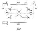
- FIG. 1 represents an example of cell C for a RAM memory. It is formed by two inverters, produced in the form of a parallel mounting of two series transistors of types p and n. The supply potentials V dd and V ss are applied to the terminals of this parallel arrangement.
- the branches of the cell include a transistor p, respectively P1 and P2, in series with a transistor n respectively N1 and N2, the gates of transistors being interconnected by connections crossed as shown in Figure 1.
- Cell C also includes transistors selection S1 and S2 which are intended to ensure respectively connecting the branches of the cell to bit lines oriented according to the columns of the memory matrix and called one (bl1) "direct bit line” and the other (bl2) "reverse bit line”.
- the control of transistors S1 and S2 is ensured, in common for all cells in a row of memory and in a manner known per se, through the addressing which generates the selection signals Sel1 and Sel2.
- Data read and write operations in cells are made through the lines of bits bll and bl2 by reading control means R and writing W, symbolized in FIG. 1 by rectangles, it being understood that according to the invention, the bit line bl1 is commanded in read and write and the bit line bl2 in writing only.
- Figure 2 shows in more detail the mode of preferred embodiment of the memory according to the invention, and more precisely the organization of a single column of this memory RAM, the column being formed by a large number of C cells.
- C cells are symbolized by two inverters head to tail and we only drew a number reduced.
- Memory can include a juxtaposition of a very many of these columns.
- C cells are connected to lines of direct and reverse bits bl1 and bl2.
- bit line bl1 is split into a plurality of line sections 1.
- a group of C cells is connected, these being by elsewhere all connected to the other bit line bl2 which, here it is not split.
- the splitting into sections is performed for groups of equivalent cells located in the same rows of the memory array.
- each addressed cell frees itself from the symmetry of memory cells.
- the control of each addressed cell is carried out from such that the write operation in a cell is do through the two selection transistors S1 and S2, but that the reading operation in a cell is not done only through one of the transistors S1 or S2 only, depending on the logic adopted for memory.
- T N2 T N1 / 3.2
- T S1 T N1
- the sections 1 of the bit line bl1 are connected to the Entrances of an exit door 2 ensuring the presentation of read signals on its output 3.
- the logic function of this door is advantageously NAND, with the chosen logic for this memory, but another function can, of course, be chosen if this logic adopted is different.
- Each of sections 1 of the split bit line bll is also connected to a p-type transistor 4 ensuring its preload and to another n-type control transistor 5.
- the gates of the transistors 4 are connected together to a first control logic LC1 ensuring, depending on whether it is a write or read operation, the function Sel.WD or Sel. W , where "Sel” is the selection signal, "W” the write signal, W the read signal, and “D” the data signal, the symbol “.” representing the "AND” logic function.
- the gates of the transistors 5 are connected together to a second LC2 control logic ensuring the function logic Sel.W.D, whether it is a write operation or of reading.
- the sections 1 of the bit line bl1 are always preloaded at V DD when no cell of the column is addressed, the transistor p 4 being conductive with its gate brought to V SS . It is therefore a waiting situation for each column of the memory.
- the Sel signal goes high. If it is a write, the signal W goes high, the transistor 4 of the section 1 concerned by the addressed cell then establishing the level of the potential V DD on this section 1, if the data signal D is low. On the other hand, if the data signal D is high, the transistor 5 passes the section 1 to the potential V SS . The corresponding bit line receives the complementary value of the data signal D.
- bit line bl2 The waiting condition for bit line bl2 is that of low level. It is only brought to the high level if a signal from data is high while writing to a column cell considered. Indeed, this line is not connected to a cell addressed by the selection transistor S2 only during writing. On the other hand, during reading, this transistor is not activated, this which reduces consumption.
- write and read command as just described can also be applied to RAM memories of which in each column, the bit lines neither such a memory is split can then include asymmetric cells with dimension reports as described above.
- the invention is not limited to types of logic described.
Landscapes
- Engineering & Computer Science (AREA)
- Microelectronics & Electronic Packaging (AREA)
- Computer Hardware Design (AREA)
- Static Random-Access Memory (AREA)
- Surgical Instruments (AREA)
- Memory System Of A Hierarchy Structure (AREA)
- Electrophonic Musical Instruments (AREA)
- Valve Device For Special Equipments (AREA)
Abstract
Description
- la figure 1 est un schéma d'une cellule d'une mémoire RAM selon l'invention;
- la figure 2 est un schéma partiel du mode de réalisation préféré d'une mémoire RAM selon l'invention.
Claims (5)
- Mémoire RAM comportant une matrice composée de cellules agencées en rangées et en colonnes et dans laquelle les cellules sont adressables par rangées, chaque cellule d'une rangée étant connectée à des première et deuxième lignes de bits dont au moins ladite première ligne (bl1) est fractionnée, ladite première ligne de bits fractionnée présentant une pluralité de tronçons (1) connectés respectivement aux entrées d'une porte logique de sortie (2,3),
la mémoire comprenant également des moyens de commande de lecture/écriture,
cette mémoire étant caractérisée en ce que lesdits moyens de commande (LC1, LC2) de lecture/écriture sont agencés pour directement ou indirectement appliquer, sélectivement selon qu'il s'agit d'une opération d'écriture ou de lecture, à chacune desdites première et deuxième lignes de bits (bl1, bl2), les fonctions logiques suivantes :Sel.((W.D) ouW )) sur ladite première ligne de bits (bl1), pendant que Sel.W.D est appliqué sur lesdites première et deuxième lignes de bits (bl1, bl2), et"Sel" étant un signal de sélection de cellule représentatif de l'adressage, "W" étant la commande d'écriture,W étant la commande de lecture, "D" étant la donnée à écrire dans la cellule adressée et "." étant le symbole de la fonction ET. - Mémoire RAM selon la revendication 1, caractérisée en ce que chacun desdits tronçons (1) est raccordé à deux transistors (4, 5) de types de conductivité opposés, et en ce que lesdites fonctions logiques sont appliquées sélectivement sur les grilles desdits transistors.
- Mémoire RAM selon l'une quelconque des revendications 1 et 2, dans laquelle chacune desdites cellules comprend deux branches composées chacune de deux transistors en série de types de conductivité opposés (P1, N1, P2, N2) dont les grilles sont connectées ensemble, respectivement par des conducteurs croisés, chaque cellule comprenant également des transistors de sélection (Si, S2) connectés respectivement auxdites branches et lesdites lignes de bits pour permettre la sélection de la cellule en fonction de l'adressage de la mémoire, caractérisée en ce que les transistors (P1, P2) de la branche susceptible d'être connectée au tronçon (1) de ligne de bits correspondant, ont une taille supérieure à celle des transistors (P2, N2) de l'autre branche.
- Mémoire RAM selon l'une quelconque des revendications 1 à 3, caractérisée en ce que chacun desdits tronçons (1) est connecté à des moyens de précharge (4).
- Mémoire RAM selon l'une quelconque des revendications 1 à 4, caractérisée en ce que ladite porte de sortie (2, 3) est une porte NON-ET.
Applications Claiming Priority (2)
| Application Number | Priority Date | Filing Date | Title |
|---|---|---|---|
| FR9908947A FR2808114B1 (fr) | 1999-07-09 | 1999-07-09 | Memoire ram |
| FR9908947 | 1999-07-09 |
Publications (2)
| Publication Number | Publication Date |
|---|---|
| EP1067556A1 true EP1067556A1 (fr) | 2001-01-10 |
| EP1067556B1 EP1067556B1 (fr) | 2005-10-19 |
Family
ID=9547944
Family Applications (1)
| Application Number | Title | Priority Date | Filing Date |
|---|---|---|---|
| EP00401972A Expired - Lifetime EP1067556B1 (fr) | 1999-07-09 | 2000-07-07 | Mémoire RAM |
Country Status (5)
| Country | Link |
|---|---|
| US (1) | US6366504B1 (fr) |
| EP (1) | EP1067556B1 (fr) |
| AT (1) | ATE307377T1 (fr) |
| DE (1) | DE60023213T2 (fr) |
| FR (1) | FR2808114B1 (fr) |
Families Citing this family (3)
| Publication number | Priority date | Publication date | Assignee | Title |
|---|---|---|---|---|
| US6580635B1 (en) * | 2002-04-25 | 2003-06-17 | Hewlett-Packard Development Company, L.P. | Bitline splitter |
| US6657886B1 (en) * | 2002-05-07 | 2003-12-02 | International Business Machines Corporation | Split local and continuous bitline for fast domino read SRAM |
| US6741493B1 (en) * | 2002-11-07 | 2004-05-25 | International Business Machines Corporation | Split local and continuous bitline requiring fewer wires |
Citations (4)
| Publication number | Priority date | Publication date | Assignee | Title |
|---|---|---|---|---|
| US5729501A (en) * | 1995-09-08 | 1998-03-17 | International Business Machines Corporation | High Speed SRAM with or-gate sense |
| US5850367A (en) * | 1996-11-29 | 1998-12-15 | Mitsubishi Denki Kabushiki Kaisha | Static type semiconductor memory with latch circuit amplifying read data read on a sub bit line pair and transferring the amplified read data to a main bit line pair and operation method thereof |
| US5901079A (en) * | 1997-01-13 | 1999-05-04 | International Business Machines Corporation | Skewed memory cell apparatus and method |
| US5966320A (en) * | 1998-03-13 | 1999-10-12 | Winbond Electronics Corp. | SRAM structure having common bit line |
Family Cites Families (2)
| Publication number | Priority date | Publication date | Assignee | Title |
|---|---|---|---|---|
| EP0920027B1 (fr) * | 1997-11-28 | 2004-03-03 | STMicroelectronics S.r.l. | Cellule de mémoire RAM à consommation réduite avec une seule ligne de bit |
| US6240009B1 (en) * | 2000-02-02 | 2001-05-29 | Hewlett-Packard Company | Asymmetric ram cell |
-
1999
- 1999-07-09 FR FR9908947A patent/FR2808114B1/fr not_active Expired - Fee Related
-
2000
- 2000-07-07 US US09/612,061 patent/US6366504B1/en not_active Expired - Lifetime
- 2000-07-07 DE DE60023213T patent/DE60023213T2/de not_active Expired - Lifetime
- 2000-07-07 EP EP00401972A patent/EP1067556B1/fr not_active Expired - Lifetime
- 2000-07-07 AT AT00401972T patent/ATE307377T1/de not_active IP Right Cessation
Patent Citations (4)
| Publication number | Priority date | Publication date | Assignee | Title |
|---|---|---|---|---|
| US5729501A (en) * | 1995-09-08 | 1998-03-17 | International Business Machines Corporation | High Speed SRAM with or-gate sense |
| US5850367A (en) * | 1996-11-29 | 1998-12-15 | Mitsubishi Denki Kabushiki Kaisha | Static type semiconductor memory with latch circuit amplifying read data read on a sub bit line pair and transferring the amplified read data to a main bit line pair and operation method thereof |
| US5901079A (en) * | 1997-01-13 | 1999-05-04 | International Business Machines Corporation | Skewed memory cell apparatus and method |
| US5966320A (en) * | 1998-03-13 | 1999-10-12 | Winbond Electronics Corp. | SRAM structure having common bit line |
Non-Patent Citations (1)
| Title |
|---|
| HIROYUKI HARA ET AL: "0.5-UM 2M-TRANSISTOR BIPNMOS CHANNELLESS GATE ARRAY", IEEE JOURNAL OF SOLID-STATE CIRCUITS,US,IEEE INC. NEW YORK, vol. 26, no. 11, 1 November 1991 (1991-11-01), pages 1615 - 1620, XP000266671, ISSN: 0018-9200 * |
Also Published As
| Publication number | Publication date |
|---|---|
| DE60023213T2 (de) | 2006-07-06 |
| US6366504B1 (en) | 2002-04-02 |
| ATE307377T1 (de) | 2005-11-15 |
| FR2808114A1 (fr) | 2001-10-26 |
| EP1067556B1 (fr) | 2005-10-19 |
| FR2808114B1 (fr) | 2002-07-12 |
| DE60023213D1 (de) | 2006-03-02 |
Similar Documents
| Publication | Publication Date | Title |
|---|---|---|
| FR2774209A1 (fr) | Procede de controle du circuit de lecture d'un plan memoire et dispositif de memoire correspondant | |
| FR2898432A1 (fr) | Cellules memoire en technologie cmos double-grille dotee de transistors a deux grilles independantes | |
| FR3074604A1 (fr) | Memoire sram a effacement rapide | |
| EP1388896A1 (fr) | Mémoire sur substrat du type silicium sur isolant. | |
| EP3598451B1 (fr) | Memoire sram / rom reconfigurable par connexions aux alimentations | |
| EP3382709B1 (fr) | Cellule mémoire sram | |
| EP2073212B1 (fr) | Dispositif de lecture d'une mémoire non volatile à basse consommation, et son procédé de mise en action | |
| FR2729782A1 (fr) | Cellule de memoire a cinq transistors comportant une ligne d'alimentation en energie partagee | |
| FR2775382A1 (fr) | Procede de controle du rafraichissement d'un plan memoire d'un dispositif de memoire vive dynamique, et dispositif de memoire vive correspondant | |
| EP1067556B1 (fr) | Mémoire RAM | |
| EP0660331B1 (fr) | Circuit décodeur de ligne pour mémoire fonctionnant sous de faibles tensions d'alimentation | |
| FR2986652A1 (fr) | Memoire volatile a consommation reduite et capacite de stockage amelioree | |
| EP3680904B1 (fr) | Circuit de detection de donnee predominante dans une cellule memoire | |
| FR2787212A1 (fr) | Circuit pour remettre a l'etat initial une paire de bus de donnees d'un dispositif de memoire a semiconducteur | |
| FR2828758A1 (fr) | Procede d'ecriture dans une memoire ram comportant un systeme d'effacement de colonnes | |
| FR2811132A1 (fr) | Circuit de memoire dynamique comportant des cellules de secours | |
| FR2810150A1 (fr) | Dispositif de memoire vive dynamique et procede de commande d'un acces en lecture d'une telle memoire | |
| EP1168359B1 (fr) | Procédé de commande d'un accès en lecture d'une mémoire vive dynamique et mémoire correspondante. | |
| FR3061798B1 (fr) | Circuit de commande d'une ligne d'une matrice memoire | |
| EP3503105B1 (fr) | Circuit mémoire partitionné adapté à mettre en oeuvre des opérations de calcul | |
| WO2009034156A2 (fr) | Point memoire de memoire statique et application a un capteur d'image | |
| EP3598450B1 (fr) | Memoire sram a courants de fuite reduits | |
| FR3167241A1 (fr) | Circuit mémoire à cellules FeRAM double port | |
| WO2001091130A1 (fr) | Memoire rom de taille reduite | |
| FR2976114A1 (fr) | Memoire double port permettant une lecture-ecriture simultanee |
Legal Events
| Date | Code | Title | Description |
|---|---|---|---|
| PUAI | Public reference made under article 153(3) epc to a published international application that has entered the european phase |
Free format text: ORIGINAL CODE: 0009012 |
|
| AK | Designated contracting states |
Kind code of ref document: A1 Designated state(s): AT BE CH CY DE DK ES FI FR GB GR IE IT LI LU MC NL PT SE |
|
| AX | Request for extension of the european patent |
Free format text: AL;LT;LV;MK;RO;SI |
|
| 17P | Request for examination filed |
Effective date: 20010605 |
|
| AKX | Designation fees paid |
Free format text: AT BE CH CY DE DK ES FI FR GB GR IE IT LI LU MC NL PT SE |
|
| GRAP | Despatch of communication of intention to grant a patent |
Free format text: ORIGINAL CODE: EPIDOSNIGR1 |
|
| GRAS | Grant fee paid |
Free format text: ORIGINAL CODE: EPIDOSNIGR3 |
|
| GRAA | (expected) grant |
Free format text: ORIGINAL CODE: 0009210 |
|
| RAP1 | Party data changed (applicant data changed or rights of an application transferred) |
Owner name: CSEM CENTRE SUISSE D'ELECTRONIQUE ET DEMICROTECHNI |
|
| AK | Designated contracting states |
Kind code of ref document: B1 Designated state(s): AT BE CH CY DE DK ES FI FR GB GR IE IT LI LU MC NL PT SE |
|
| PG25 | Lapsed in a contracting state [announced via postgrant information from national office to epo] |
Ref country code: IT Free format text: LAPSE BECAUSE OF FAILURE TO SUBMIT A TRANSLATION OF THE DESCRIPTION OR TO PAY THE FEE WITHIN THE PRE;WARNING: LAPSES OF ITALIAN PATENTS WITH EFFECTIVE DATE BEFORE 2007 MAY HAVE OCCURRED AT ANY TIME BEFORE 2007. THE CORRECT EFFECTIVE DATE MAY BE DIFFERENT FROM THE ONE RECORDED.SCRIBED TIME-LIMIT Effective date: 20051019 Ref country code: AT Free format text: LAPSE BECAUSE OF FAILURE TO SUBMIT A TRANSLATION OF THE DESCRIPTION OR TO PAY THE FEE WITHIN THE PRESCRIBED TIME-LIMIT Effective date: 20051019 Ref country code: IE Free format text: LAPSE BECAUSE OF FAILURE TO SUBMIT A TRANSLATION OF THE DESCRIPTION OR TO PAY THE FEE WITHIN THE PRESCRIBED TIME-LIMIT Effective date: 20051019 Ref country code: NL Free format text: LAPSE BECAUSE OF FAILURE TO SUBMIT A TRANSLATION OF THE DESCRIPTION OR TO PAY THE FEE WITHIN THE PRESCRIBED TIME-LIMIT Effective date: 20051019 Ref country code: FI Free format text: LAPSE BECAUSE OF FAILURE TO SUBMIT A TRANSLATION OF THE DESCRIPTION OR TO PAY THE FEE WITHIN THE PRESCRIBED TIME-LIMIT Effective date: 20051019 |
|
| REG | Reference to a national code |
Ref country code: GB Ref legal event code: FG4D Free format text: NOT ENGLISH |
|
| REG | Reference to a national code |
Ref country code: CH Ref legal event code: EP |
|
| REG | Reference to a national code |
Ref country code: IE Ref legal event code: FG4D Free format text: LANGUAGE OF EP DOCUMENT: FRENCH |
|
| PG25 | Lapsed in a contracting state [announced via postgrant information from national office to epo] |
Ref country code: GR Free format text: LAPSE BECAUSE OF FAILURE TO SUBMIT A TRANSLATION OF THE DESCRIPTION OR TO PAY THE FEE WITHIN THE PRESCRIBED TIME-LIMIT Effective date: 20060119 Ref country code: DK Free format text: LAPSE BECAUSE OF FAILURE TO SUBMIT A TRANSLATION OF THE DESCRIPTION OR TO PAY THE FEE WITHIN THE PRESCRIBED TIME-LIMIT Effective date: 20060119 Ref country code: SE Free format text: LAPSE BECAUSE OF FAILURE TO SUBMIT A TRANSLATION OF THE DESCRIPTION OR TO PAY THE FEE WITHIN THE PRESCRIBED TIME-LIMIT Effective date: 20060119 |
|
| PG25 | Lapsed in a contracting state [announced via postgrant information from national office to epo] |
Ref country code: ES Free format text: LAPSE BECAUSE OF FAILURE TO SUBMIT A TRANSLATION OF THE DESCRIPTION OR TO PAY THE FEE WITHIN THE PRESCRIBED TIME-LIMIT Effective date: 20060130 |
|
| GBT | Gb: translation of ep patent filed (gb section 77(6)(a)/1977) |
Effective date: 20060108 |
|
| REF | Corresponds to: |
Ref document number: 60023213 Country of ref document: DE Date of ref document: 20060302 Kind code of ref document: P |
|
| PG25 | Lapsed in a contracting state [announced via postgrant information from national office to epo] |
Ref country code: PT Free format text: LAPSE BECAUSE OF FAILURE TO SUBMIT A TRANSLATION OF THE DESCRIPTION OR TO PAY THE FEE WITHIN THE PRESCRIBED TIME-LIMIT Effective date: 20060320 |
|
| NLV1 | Nl: lapsed or annulled due to failure to fulfill the requirements of art. 29p and 29m of the patents act | ||
| REG | Reference to a national code |
Ref country code: IE Ref legal event code: FD4D |
|
| PG25 | Lapsed in a contracting state [announced via postgrant information from national office to epo] |
Ref country code: BE Free format text: LAPSE BECAUSE OF NON-PAYMENT OF DUE FEES Effective date: 20060731 Ref country code: MC Free format text: LAPSE BECAUSE OF NON-PAYMENT OF DUE FEES Effective date: 20060731 |
|
| PLBE | No opposition filed within time limit |
Free format text: ORIGINAL CODE: 0009261 |
|
| STAA | Information on the status of an ep patent application or granted ep patent |
Free format text: STATUS: NO OPPOSITION FILED WITHIN TIME LIMIT |
|
| 26N | No opposition filed |
Effective date: 20060720 |
|
| REG | Reference to a national code |
Ref country code: CH Ref legal event code: NV Representative=s name: GLN S.A. |
|
| BERE | Be: lapsed |
Owner name: CSEM CENTRE SUISSE D'ELECTRONIQUE ET DE MICROTECH Effective date: 20060731 |
|
| PG25 | Lapsed in a contracting state [announced via postgrant information from national office to epo] |
Ref country code: LU Free format text: LAPSE BECAUSE OF NON-PAYMENT OF DUE FEES Effective date: 20060707 |
|
| PG25 | Lapsed in a contracting state [announced via postgrant information from national office to epo] |
Ref country code: CY Free format text: LAPSE BECAUSE OF FAILURE TO SUBMIT A TRANSLATION OF THE DESCRIPTION OR TO PAY THE FEE WITHIN THE PRESCRIBED TIME-LIMIT Effective date: 20051019 |
|
| REG | Reference to a national code |
Ref country code: CH Ref legal event code: PCAR Free format text: NEW ADDRESS: AVENUE EDOUARD-DUBOIS 20, 2000 NEUCHATEL (CH) |
|
| REG | Reference to a national code |
Ref country code: FR Ref legal event code: PLFP Year of fee payment: 17 |
|
| REG | Reference to a national code |
Ref country code: CH Ref legal event code: PFA Owner name: CSEM CENTRE SUISSE D'ELECTRONIQUE ET DE MICROT, CH Free format text: FORMER OWNER: CSEM CENTRE SUISSE D'ELECTRONIQUE ET DE MICROTECHNIQUE S.A. - RECHERCHE ET DEVELOPPEMENT, CH |
|
| REG | Reference to a national code |
Ref country code: FR Ref legal event code: PLFP Year of fee payment: 18 |
|
| REG | Reference to a national code |
Ref country code: FR Ref legal event code: PLFP Year of fee payment: 19 |
|
| PGFP | Annual fee paid to national office [announced via postgrant information from national office to epo] |
Ref country code: DE Payment date: 20180727 Year of fee payment: 19 Ref country code: FR Payment date: 20180730 Year of fee payment: 19 |
|
| PGFP | Annual fee paid to national office [announced via postgrant information from national office to epo] |
Ref country code: GB Payment date: 20180730 Year of fee payment: 19 Ref country code: CH Payment date: 20180730 Year of fee payment: 19 |
|
| REG | Reference to a national code |
Ref country code: CH Ref legal event code: NV Representative=s name: BOVARD SA NEUCHATEL CONSEILS EN PROPRIETE INTE, CH |
|
| REG | Reference to a national code |
Ref country code: DE Ref legal event code: R119 Ref document number: 60023213 Country of ref document: DE |
|
| REG | Reference to a national code |
Ref country code: CH Ref legal event code: PL |
|
| GBPC | Gb: european patent ceased through non-payment of renewal fee |
Effective date: 20190707 |
|
| PG25 | Lapsed in a contracting state [announced via postgrant information from national office to epo] |
Ref country code: GB Free format text: LAPSE BECAUSE OF NON-PAYMENT OF DUE FEES Effective date: 20190707 Ref country code: DE Free format text: LAPSE BECAUSE OF NON-PAYMENT OF DUE FEES Effective date: 20200201 |
|
| PG25 | Lapsed in a contracting state [announced via postgrant information from national office to epo] |
Ref country code: LI Free format text: LAPSE BECAUSE OF NON-PAYMENT OF DUE FEES Effective date: 20190731 Ref country code: CH Free format text: LAPSE BECAUSE OF NON-PAYMENT OF DUE FEES Effective date: 20190731 |
|
| PG25 | Lapsed in a contracting state [announced via postgrant information from national office to epo] |
Ref country code: FR Free format text: LAPSE BECAUSE OF NON-PAYMENT OF DUE FEES Effective date: 20190731 |