EP1061703A2 - Schaltungsanordnung zur Übertragung von Impulsen über eine Übertragungsstrecke - Google Patents
Schaltungsanordnung zur Übertragung von Impulsen über eine Übertragungsstrecke Download PDFInfo
- Publication number
- EP1061703A2 EP1061703A2 EP00111388A EP00111388A EP1061703A2 EP 1061703 A2 EP1061703 A2 EP 1061703A2 EP 00111388 A EP00111388 A EP 00111388A EP 00111388 A EP00111388 A EP 00111388A EP 1061703 A2 EP1061703 A2 EP 1061703A2
- Authority
- EP
- European Patent Office
- Prior art keywords
- transmission
- flop
- pulses
- toggle flip
- output
- Prior art date
- Legal status (The legal status is an assumption and is not a legal conclusion. Google has not performed a legal analysis and makes no representation as to the accuracy of the status listed.)
- Withdrawn
Links
Images


Classifications
-
- H—ELECTRICITY
- H04—ELECTRIC COMMUNICATION TECHNIQUE
- H04L—TRANSMISSION OF DIGITAL INFORMATION, e.g. TELEGRAPHIC COMMUNICATION
- H04L25/00—Baseband systems
- H04L25/02—Details ; arrangements for supplying electrical power along data transmission lines
- H04L25/08—Modifications for reducing interference; Modifications for reducing effects due to line faults ; Receiver end arrangements for detecting or overcoming line faults
Definitions
- the invention relates to a circuit arrangement for transmission of pulses over a transmission path.
- Another option is to transfer the one to be transferred short pulse with the help of a multi-stage delay circuit, as shown in Figure 1 to extend.
- To the short pulses S1 to be transmitted become direct on the one hand on the first input of an OR gate OR1 and on the other via a delay element V to the second input of the OR gate OR1 performed.
- At the output of the OR gate OR1 one then obtains pulses extended by the delay time ⁇ t S3, which is then a second delay stage, which in Structure corresponds to the first delay stage supplied is, so that at the output of the second OR gate OR2 a the delay time 2 * ⁇ t extended pulse S4 available stands.
- the corresponding signal profiles are shown in Figure 2. With very short input pulses S1 must the signal processing takes place in several stages, because the OR gate for time delays ⁇ t that are larger than the pulse width are, unwanted double pulses are generated. Unfortunately increases with each additional delay stage required the power loss and the required chip area on.
- JP-63-227113-A is a circuit arrangement for the transmission of pulses with a frequency divider, which has two flip-flops and a frequency multiplier, which has an EXOR gate, is known.
- An object of the invention is to avoid the above Disadvantages mentioned a circuit arrangement for transmission of impulses over a long transmission distance.
- the circuit arrangement according to the invention for the transmission of Pulses over a transmission link have a frequency divider at the input of which the pulses to be transmitted apply and its output connected to the transmission link is.
- a frequency multiplier is provided whose input is connected to the transmission link and the transmitted pulses are present at the output.
- the frequency divider having a first toggle flip-flop is easy to implement.
- the frequency divider points to this additionally a second toggle flip-flop, whereby at the clock input of the first toggle flip-flop the ones to be transmitted There are pulses and the output of the first toggle flip-flop is connected to the transmission link. Farther are at the clock input of the second toggle flip-flop to be transmitted inverted on. This is the Toggle flip-flops an amplifier with complementary outputs upstream. The output of the second toggle flip-flop is also connected to the transmission link.
- the frequency multiplier has an EXOR gate, on the first and second input connected to the transmission link is. The transmitted signal is at the output of the EXOR gate tapped.
- the amplifier upstream of the toggle flip-flops with complementary ones Outputs has the advantage that the toggle flip-flops can be of the same edge control type. Consequently the triggering of the two toggle flip-flops can either be on the low / high edge (positive edge triggered) or on the High / low edge (negative edge triggered), each for both Toggle flip-flops are the same. As a consequence, that the switching times of the two toggle flip-flops are the same and thus with short pulses the pulse width at inputs and Output matches.
- the toggle flip-flop by a simple flank-triggered D flip-flop implemented his.
- the circuit arrangement according to the invention is advantageous usable in an integrated circuit.
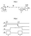
- the circuit arrangement for pulse transmission shown in FIG. 3 has a first toggle flip-flop TF1, at whose clock input the pulses S1 to be transmitted are present.
- the toggle flip-flop TF1 in FIG. 3 is implemented by a single-edge triggered D flip-flop, the inverting output of which Q is connected to the D input of the D flip-flop.
- a signal S5 is present at the output Q of the toggle flip-flop TF1 whose level with each positive edge of the input signal S1 changes.
- Signal S5 is shown in Figure 4.
- the exit Q The toggle flip-flop TF1 is connected to both the first input an exclusive OR gate EXOR as well as a delay element V with the second input of the exclusive OR gate EXOR connected. This is at the output of the EXOR gate transmitted signal S7 shown in FIG.
- the pulse width of the signal S7 corresponds to the delay period .DELTA.t of Delay element V.
- the pulse duration of the transmitted on the transmission link ÜS Signal S5 is extended so that it is the period of the applied at the input of the circuit arrangement Corresponds to signal S1.
- the pulse width of the signal present at the output of the EXOR gate S7 can be set via the delay element V. Consequently the pulse width can be easily created of the signal S7, which at the output of the EXOR gate applies to the requirements of the following - not shown - To be able to adapt circuits.
- the Outputs of the two toggle flip-flops are TF1 and TF2, respectively connected to the transmission link ÜS.
- the transmission link In the present case, ÜS has two lines on.
- the transmission link is on the other hand with the two Inputs of the EXOR gate connected.
- the signal S9 can be tapped in terms of pulse width and period duration is the same as the input signal S1.
- the output of the toggle flip-flop TF1 changes level with the rising edge of the input signal S1 while with the toggle flip-flop TF2 the output level with the falling Edge of the input signal S1 changes.
- the toggle flip-flops TF1 and TF2 is an exact replica of the Input signal S1 possible.
- FIGS. 3 and 5 shown in FIGS Circuit arrangement according to the invention for the transmission of pulses have the advantage that no high performance drivers are required are.
- the current requirement can be at an input signal frequency of around 8 GHz can be up to 20 times lower than the current requirement as it is in the prior art as described in the introduction necessary is.
- circuit arrangement according to the invention can transmit impulses of any length over longer distances become.
- circuit arrangement according to the invention jitter free.
- the power savings in the circuit arrangement according to the invention has a more positive effect the smaller the duty cycle for the signal to be transmitted is S1, so the smaller is the ratio of impulse to pause duration.
Landscapes
- Engineering & Computer Science (AREA)
- Power Engineering (AREA)
- Computer Networks & Wireless Communication (AREA)
- Signal Processing (AREA)
- Dc Digital Transmission (AREA)
- Manipulation Of Pulses (AREA)
- Cable Transmission Systems, Equalization Of Radio And Reduction Of Echo (AREA)
Abstract
Description
- Figur 1
- zeigt eine Schaltung zur Impulsverbreitung gemäß dem Stand der Technik.
- Figur 2
- zeigt die zu Figur 1 korrespondierenden Signalverläufe.
- Figur 3
- zeigt eine erste erfindungsgemäße Ausführungsform der Schaltungsanordnung zur Übertragung von Impulsen.
- Figur 4
- zeigt die zu Figur 3 korrespondierenden Signalverläufe.
- Figur 5
- zeigt eine zweite erfindungsgemäße Ausführungsform der Schaltungsanordnung zur Übertragung von Impulsen.
- Figur 6
- zeigt die zu Figur 5 korrespondierenden Signalverläufe.
Claims (3)
- Schaltungsanordnung zur Übertragung von Impulsen über eine Übertragungsstrecke,mit einem Frequenzteiler, an dessen Eingang die zu übertragenden Impulse (S1) anliegen und dessen Ausgang mit der Übertragungsstrecke (ÜS) verbunden ist,mit einem Frequenzvervielfacher, dessen Eingang mit der Übertragungsstrecke (ÜS) verbunden ist und an dessen Ausgang die übertragenen Impulse (S7, S9) anliegen,bei der der Frequenzteiler ein erstes Toggle-Flip-Flop (TF1) und ein zweites Toggle-Flip-Flop (TF2), welches vom gleichen Flankensteuerungstyp wie das erste Toggle-Flip-Flop (TF1) ist, aufweist,
wobei am Takteingang des ersten Toggle-Flip-Flops (TF1) die zu übertragenden Impulse (S1) anliegen und dessen Ausgang mit der Übertragungsstrecke (ÜS) verbunden ist,
wobei am Takteingang des zweiten Toggle-Flip-Flops (TF2) die zu übertragenden Impulse (S1) invertiert anliegen, und dessen Ausgang mit der Übertragungsstrecke (ÜS) verbunden ist,bei der der Frequenzvervielfacher ein EXOR-Gatter (EXOR) aufweist, dessen erster und zweiter Eingang mit der Übertragungsstrecke (ÜS) verbunden ist, und
wobei die zu übertragenden Impulse (S1) einem Verstärker mit komplementären Ausgängen zuführbar sind, wobei je ein Ausgang des Verstärkers mit je einem Takteingang der Toggle-Flip-Flops (TF1, TF2) verbunden ist. - Schaltungsanordnung nach Anspruch 1,bei der das Toggle-Flip-Flop (TF1) durch ein einflankengetriggertes D-Flip-Flop realisiert ist.
- Verwendung der Schaltungsanordnung nach Anspruch 1 oder 2, in einem integrierten Schaltkreis.
Applications Claiming Priority (2)
| Application Number | Priority Date | Filing Date | Title |
|---|---|---|---|
| DE19927587 | 1999-06-16 | ||
| DE19927587 | 1999-06-16 |
Publications (2)
| Publication Number | Publication Date |
|---|---|
| EP1061703A2 true EP1061703A2 (de) | 2000-12-20 |
| EP1061703A3 EP1061703A3 (de) | 2003-12-03 |
Family
ID=7911508
Family Applications (1)
| Application Number | Title | Priority Date | Filing Date |
|---|---|---|---|
| EP00111388A Withdrawn EP1061703A3 (de) | 1999-06-16 | 2000-05-26 | Schaltungsanordnung zur Übertragung von Impulsen über eine Übertragungsstrecke |
Country Status (2)
| Country | Link |
|---|---|
| US (1) | US6741657B1 (de) |
| EP (1) | EP1061703A3 (de) |
Cited By (1)
| Publication number | Priority date | Publication date | Assignee | Title |
|---|---|---|---|---|
| WO2015172942A1 (de) * | 2014-05-15 | 2015-11-19 | Ifm Electronic Gmbh | Elektronische schaltung zur steuerung eines aktors |
Families Citing this family (1)
| Publication number | Priority date | Publication date | Assignee | Title |
|---|---|---|---|---|
| EP2665225B1 (de) * | 2011-01-13 | 2018-04-11 | Mitsubishi Electric Corporation | Bit-erzeugungsvorrichtung und bit-erzeugungsverfahren |
Family Cites Families (5)
| Publication number | Priority date | Publication date | Assignee | Title |
|---|---|---|---|---|
| DE2529448C2 (de) * | 1975-07-02 | 1984-02-09 | Felten & Guilleaume Fernmeldeanlagen GmbH, 8500 Nürnberg | Schaltungsanordnung zur Umwandlung von NRZ-Signalen in RZ-Signale, insbesondere für die synchrone Zeitmultiplexbildung |
| US4516236A (en) * | 1983-09-26 | 1985-05-07 | Northern Telecom Limited | Full-duplex transmission of bit streams serially and in bit-synchronism on a bus between two terminals. |
| JPS63227113A (ja) * | 1987-03-16 | 1988-09-21 | Nec Corp | 伝播回路 |
| DE4020719A1 (de) * | 1990-06-29 | 1992-01-02 | Broadcast Television Syst | Verfahren zur uebertragung eines digitalen datensignals |
| JP3508412B2 (ja) * | 1995-08-10 | 2004-03-22 | セイコーエプソン株式会社 | データ復号回路、電圧制御発振回路、データ復号装置及び電子機器 |
-
2000
- 2000-05-26 EP EP00111388A patent/EP1061703A3/de not_active Withdrawn
- 2000-06-14 US US09/593,403 patent/US6741657B1/en not_active Expired - Lifetime
Cited By (2)
| Publication number | Priority date | Publication date | Assignee | Title |
|---|---|---|---|---|
| WO2015172942A1 (de) * | 2014-05-15 | 2015-11-19 | Ifm Electronic Gmbh | Elektronische schaltung zur steuerung eines aktors |
| US10333735B2 (en) | 2014-05-15 | 2019-06-25 | Ifm Electronic Gmbh | Electronic circuit for controlling an actuator |
Also Published As
| Publication number | Publication date |
|---|---|
| US6741657B1 (en) | 2004-05-25 |
| EP1061703A3 (de) | 2003-12-03 |
Similar Documents
| Publication | Publication Date | Title |
|---|---|---|
| DE10043761C2 (de) | HF-Verteilnetz | |
| DE2047001C3 (de) | Anordnungen für die Übertragung von Daten innerhalb einer Datenverarbeitungsanlage | |
| EP0059802B1 (de) | Integrierte Isolierschicht-Feldeffekttransistor-Verzögerungsschaltung für Digitalsignale und deren Verwendung in Farbfernsehempfängern | |
| DE3708499C2 (de) | ||
| DE3586867T2 (de) | In abhaengigkeit eines eingangssignals mit variabler datenrate betreibbarer leitungsentzerrer. | |
| DE3633310C2 (de) | ||
| DE19960785A1 (de) | Eingangsfilterstufe für einen Datenstrom und Verfahren zum Filtern eines Datenstroms | |
| DE69511628T2 (de) | Pulserzeugung | |
| EP0977406B1 (de) | Schaltungsanordnung zum galvanisch getrennten Übertragen von Digitalsignalen | |
| DE4428545A1 (de) | Schaltungsanordnung zur Umwandlung eines seriellen Datensignals in ein paralleles Datensignal | |
| EP1061703A2 (de) | Schaltungsanordnung zur Übertragung von Impulsen über eine Übertragungsstrecke | |
| DE2822359A1 (de) | Elektrisches filter | |
| EP0855798B1 (de) | Schaltungsanordnung zum Erzeugen eines Ausgangssignals | |
| DE1935411B2 (de) | Anordnung zur Tastung von periodischen Signalen | |
| DE3429982A1 (de) | Schaltungsanordnung zum uebertragen von binaeren signalen | |
| EP0141946A2 (de) | Schaltungsanordnung zum Synchronisieren der Flanken von Binärsignalen mit einem Takt | |
| DE2710270B2 (de) | Schaltungsanordnung zur Erzeugung von mit eintreffenden Datenimpulsen synchronisierten Taktimpulsen | |
| DE69533604T2 (de) | Verriegelungsschaltung | |
| EP0443117A2 (de) | Analoge Leitungsanschaltung | |
| DE19836412C2 (de) | Übertragungssystem für Digitalsignale | |
| EP0087153B1 (de) | Digitalsignal-Multiplexer für hohe Datenraten | |
| EP0392056B1 (de) | Taktsignalschaltung | |
| DE2109895C3 (de) | Schaltungsanordnung zur identischen Zeitverzögerung zweier Signale in entgegengesetzter Richtung | |
| DE19942688C2 (de) | Verfahren zum Betrieb einer elektronischen Schaltung und elektronische Schaltung | |
| EP0038509A1 (de) | Logikschaltung zum Vermeiden eines Verriegelungszustandes zwischen voneinander entfernten Datenbussen |
Legal Events
| Date | Code | Title | Description |
|---|---|---|---|
| PUAI | Public reference made under article 153(3) epc to a published international application that has entered the european phase |
Free format text: ORIGINAL CODE: 0009012 |
|
| AK | Designated contracting states |
Kind code of ref document: A2 Designated state(s): AT BE CH CY DE DK ES FI FR GB GR IE IT LI LU MC NL PT SE |
|
| AX | Request for extension of the european patent |
Free format text: AL;LT;LV;MK;RO;SI |
|
| PUAL | Search report despatched |
Free format text: ORIGINAL CODE: 0009013 |
|
| AK | Designated contracting states |
Kind code of ref document: A3 Designated state(s): AT BE CH CY DE DK ES FI FR GB GR IE IT LI LU MC NL PT SE |
|
| AX | Request for extension of the european patent |
Extension state: AL LT LV MK RO SI |
|
| RIC1 | Information provided on ipc code assigned before grant |
Ipc: 7H 04L 25/49 B Ipc: 7H 04L 25/08 A |
|
| 17P | Request for examination filed |
Effective date: 20040115 |
|
| AKX | Designation fees paid |
Designated state(s): DE FR GB |
|
| 17Q | First examination report despatched |
Effective date: 20040716 |
|
| STAA | Information on the status of an ep patent application or granted ep patent |
Free format text: STATUS: THE APPLICATION IS DEEMED TO BE WITHDRAWN |
|
| 18D | Application deemed to be withdrawn |
Effective date: 20041127 |