EP1061573A2 - Semiconductor device and method of manufacturing the same - Google Patents
Semiconductor device and method of manufacturing the same Download PDFInfo
- Publication number
- EP1061573A2 EP1061573A2 EP00305095A EP00305095A EP1061573A2 EP 1061573 A2 EP1061573 A2 EP 1061573A2 EP 00305095 A EP00305095 A EP 00305095A EP 00305095 A EP00305095 A EP 00305095A EP 1061573 A2 EP1061573 A2 EP 1061573A2
- Authority
- EP
- European Patent Office
- Prior art keywords
- insulating film
- film
- capacitor
- interlayer insulating
- semiconductor device
- Prior art date
- Legal status (The legal status is an assumption and is not a legal conclusion. Google has not performed a legal analysis and makes no representation as to the accuracy of the status listed.)
- Ceased
Links
Images










Classifications
-
- H—ELECTRICITY
- H10—SEMICONDUCTOR DEVICES; ELECTRIC SOLID-STATE DEVICES NOT OTHERWISE PROVIDED FOR
- H10B—ELECTRONIC MEMORY DEVICES
- H10B53/00—Ferroelectric RAM [FeRAM] devices comprising ferroelectric memory capacitors
- H10B53/30—Ferroelectric RAM [FeRAM] devices comprising ferroelectric memory capacitors characterised by the memory core region
-
- H—ELECTRICITY
- H10—SEMICONDUCTOR DEVICES; ELECTRIC SOLID-STATE DEVICES NOT OTHERWISE PROVIDED FOR
- H10P—GENERIC PROCESSES OR APPARATUS FOR THE MANUFACTURE OR TREATMENT OF DEVICES COVERED BY CLASS H10
- H10P14/00—Formation of materials, e.g. in the shape of layers or pillars
- H10P14/60—Formation of materials, e.g. in the shape of layers or pillars of insulating materials
- H10P14/69—Inorganic materials
- H10P14/692—Inorganic materials composed of oxides, glassy oxides or oxide-based glasses
- H10P14/6938—Inorganic materials composed of oxides, glassy oxides or oxide-based glasses the material containing at least one metal element, e.g. metal oxides, metal oxynitrides or metal oxycarbides
- H10P14/69398—Inorganic materials composed of oxides, glassy oxides or oxide-based glasses the material containing at least one metal element, e.g. metal oxides, metal oxynitrides or metal oxycarbides the material having a perovskite structure, e.g. BaTiO3
-
- H—ELECTRICITY
- H10—SEMICONDUCTOR DEVICES; ELECTRIC SOLID-STATE DEVICES NOT OTHERWISE PROVIDED FOR
- H10B—ELECTRONIC MEMORY DEVICES
- H10B53/00—Ferroelectric RAM [FeRAM] devices comprising ferroelectric memory capacitors
-
- H—ELECTRICITY
- H10—SEMICONDUCTOR DEVICES; ELECTRIC SOLID-STATE DEVICES NOT OTHERWISE PROVIDED FOR
- H10D—INORGANIC ELECTRIC SEMICONDUCTOR DEVICES
- H10D84/00—Integrated devices formed in or on semiconductor substrates that comprise only semiconducting layers, e.g. on Si wafers or on GaAs-on-Si wafers
- H10D84/01—Manufacture or treatment
- H10D84/0123—Integrating together multiple components covered by H10D12/00 or H10D30/00, e.g. integrating multiple IGBTs
- H10D84/0126—Integrating together multiple components covered by H10D12/00 or H10D30/00, e.g. integrating multiple IGBTs the components including insulated gates, e.g. IGFETs
- H10D84/0144—Manufacturing their gate insulating layers
-
- H—ELECTRICITY
- H10—SEMICONDUCTOR DEVICES; ELECTRIC SOLID-STATE DEVICES NOT OTHERWISE PROVIDED FOR
- H10D—INORGANIC ELECTRIC SEMICONDUCTOR DEVICES
- H10D84/00—Integrated devices formed in or on semiconductor substrates that comprise only semiconducting layers, e.g. on Si wafers or on GaAs-on-Si wafers
- H10D84/80—Integrated devices formed in or on semiconductor substrates that comprise only semiconducting layers, e.g. on Si wafers or on GaAs-on-Si wafers characterised by the integration of at least one component covered by groups H10D12/00 or H10D30/00, e.g. integration of IGFETs
- H10D84/82—Integrated devices formed in or on semiconductor substrates that comprise only semiconducting layers, e.g. on Si wafers or on GaAs-on-Si wafers characterised by the integration of at least one component covered by groups H10D12/00 or H10D30/00, e.g. integration of IGFETs of only field-effect components
- H10D84/83—Integrated devices formed in or on semiconductor substrates that comprise only semiconducting layers, e.g. on Si wafers or on GaAs-on-Si wafers characterised by the integration of at least one component covered by groups H10D12/00 or H10D30/00, e.g. integration of IGFETs of only field-effect components of only insulated-gate FETs [IGFET]
- H10D84/834—Integrated devices formed in or on semiconductor substrates that comprise only semiconducting layers, e.g. on Si wafers or on GaAs-on-Si wafers characterised by the integration of at least one component covered by groups H10D12/00 or H10D30/00, e.g. integration of IGFETs of only field-effect components of only insulated-gate FETs [IGFET] comprising FinFETs
-
- H—ELECTRICITY
- H10—SEMICONDUCTOR DEVICES; ELECTRIC SOLID-STATE DEVICES NOT OTHERWISE PROVIDED FOR
- H10P—GENERIC PROCESSES OR APPARATUS FOR THE MANUFACTURE OR TREATMENT OF DEVICES COVERED BY CLASS H10
- H10P14/00—Formation of materials, e.g. in the shape of layers or pillars
- H10P14/60—Formation of materials, e.g. in the shape of layers or pillars of insulating materials
- H10P14/65—Formation of materials, e.g. in the shape of layers or pillars of insulating materials characterised by treatments performed before or after the formation of the materials
- H10P14/6516—Formation of materials, e.g. in the shape of layers or pillars of insulating materials characterised by treatments performed before or after the formation of the materials of treatments performed after formation of the materials
- H10P14/6518—Formation of materials, e.g. in the shape of layers or pillars of insulating materials characterised by treatments performed before or after the formation of the materials of treatments performed after formation of the materials by introduction of substances into an already-existing insulating layer
- H10P14/6524—Formation of materials, e.g. in the shape of layers or pillars of insulating materials characterised by treatments performed before or after the formation of the materials of treatments performed after formation of the materials by introduction of substances into an already-existing insulating layer the substance being nitrogen
- H10P14/6526—Formation of materials, e.g. in the shape of layers or pillars of insulating materials characterised by treatments performed before or after the formation of the materials of treatments performed after formation of the materials by introduction of substances into an already-existing insulating layer the substance being nitrogen introduced into an oxide material, e.g. changing SiO to SiON
-
- H—ELECTRICITY
- H10—SEMICONDUCTOR DEVICES; ELECTRIC SOLID-STATE DEVICES NOT OTHERWISE PROVIDED FOR
- H10P—GENERIC PROCESSES OR APPARATUS FOR THE MANUFACTURE OR TREATMENT OF DEVICES COVERED BY CLASS H10
- H10P14/00—Formation of materials, e.g. in the shape of layers or pillars
- H10P14/60—Formation of materials, e.g. in the shape of layers or pillars of insulating materials
- H10P14/65—Formation of materials, e.g. in the shape of layers or pillars of insulating materials characterised by treatments performed before or after the formation of the materials
- H10P14/6516—Formation of materials, e.g. in the shape of layers or pillars of insulating materials characterised by treatments performed before or after the formation of the materials of treatments performed after formation of the materials
- H10P14/6529—Formation of materials, e.g. in the shape of layers or pillars of insulating materials characterised by treatments performed before or after the formation of the materials of treatments performed after formation of the materials by exposure to a gas or vapour
- H10P14/6532—Formation of materials, e.g. in the shape of layers or pillars of insulating materials characterised by treatments performed before or after the formation of the materials of treatments performed after formation of the materials by exposure to a gas or vapour by exposure to a plasma
-
- H—ELECTRICITY
- H10—SEMICONDUCTOR DEVICES; ELECTRIC SOLID-STATE DEVICES NOT OTHERWISE PROVIDED FOR
- H10P—GENERIC PROCESSES OR APPARATUS FOR THE MANUFACTURE OR TREATMENT OF DEVICES COVERED BY CLASS H10
- H10P14/00—Formation of materials, e.g. in the shape of layers or pillars
- H10P14/60—Formation of materials, e.g. in the shape of layers or pillars of insulating materials
- H10P14/65—Formation of materials, e.g. in the shape of layers or pillars of insulating materials characterised by treatments performed before or after the formation of the materials
- H10P14/6516—Formation of materials, e.g. in the shape of layers or pillars of insulating materials characterised by treatments performed before or after the formation of the materials of treatments performed after formation of the materials
- H10P14/6544—Formation of materials, e.g. in the shape of layers or pillars of insulating materials characterised by treatments performed before or after the formation of the materials of treatments performed after formation of the materials to change the morphology of the insulating materials, e.g. transformation of an amorphous layer into a crystalline layer
-
- H—ELECTRICITY
- H10—SEMICONDUCTOR DEVICES; ELECTRIC SOLID-STATE DEVICES NOT OTHERWISE PROVIDED FOR
- H10P—GENERIC PROCESSES OR APPARATUS FOR THE MANUFACTURE OR TREATMENT OF DEVICES COVERED BY CLASS H10
- H10P95/00—Generic processes or apparatus for manufacture or treatments not covered by the other groups of this subclass
-
- H—ELECTRICITY
- H10—SEMICONDUCTOR DEVICES; ELECTRIC SOLID-STATE DEVICES NOT OTHERWISE PROVIDED FOR
- H10B—ELECTRONIC MEMORY DEVICES
- H10B12/00—Dynamic random access memory [DRAM] devices
- H10B12/01—Manufacture or treatment
- H10B12/09—Manufacture or treatment with simultaneous manufacture of the peripheral circuit region and memory cells
-
- H—ELECTRICITY
- H10—SEMICONDUCTOR DEVICES; ELECTRIC SOLID-STATE DEVICES NOT OTHERWISE PROVIDED FOR
- H10D—INORGANIC ELECTRIC SEMICONDUCTOR DEVICES
- H10D1/00—Resistors, capacitors or inductors
- H10D1/60—Capacitors
- H10D1/68—Capacitors having no potential barriers
-
- H—ELECTRICITY
- H10—SEMICONDUCTOR DEVICES; ELECTRIC SOLID-STATE DEVICES NOT OTHERWISE PROVIDED FOR
- H10P—GENERIC PROCESSES OR APPARATUS FOR THE MANUFACTURE OR TREATMENT OF DEVICES COVERED BY CLASS H10
- H10P14/00—Formation of materials, e.g. in the shape of layers or pillars
- H10P14/60—Formation of materials, e.g. in the shape of layers or pillars of insulating materials
- H10P14/63—Formation of materials, e.g. in the shape of layers or pillars of insulating materials characterised by the formation processes
- H10P14/6326—Deposition processes
- H10P14/6328—Deposition from the gas or vapour phase
- H10P14/6334—Deposition from the gas or vapour phase using decomposition or reaction of gaseous or vapour phase compounds, i.e. chemical vapour deposition
- H10P14/6336—Deposition from the gas or vapour phase using decomposition or reaction of gaseous or vapour phase compounds, i.e. chemical vapour deposition in the presence of a plasma [PECVD]
-
- H—ELECTRICITY
- H10—SEMICONDUCTOR DEVICES; ELECTRIC SOLID-STATE DEVICES NOT OTHERWISE PROVIDED FOR
- H10P—GENERIC PROCESSES OR APPARATUS FOR THE MANUFACTURE OR TREATMENT OF DEVICES COVERED BY CLASS H10
- H10P14/00—Formation of materials, e.g. in the shape of layers or pillars
- H10P14/60—Formation of materials, e.g. in the shape of layers or pillars of insulating materials
- H10P14/69—Inorganic materials
- H10P14/692—Inorganic materials composed of oxides, glassy oxides or oxide-based glasses
- H10P14/6921—Inorganic materials composed of oxides, glassy oxides or oxide-based glasses containing silicon
- H10P14/69215—Inorganic materials composed of oxides, glassy oxides or oxide-based glasses containing silicon the material being a silicon oxide, e.g. SiO2
-
- H—ELECTRICITY
- H10—SEMICONDUCTOR DEVICES; ELECTRIC SOLID-STATE DEVICES NOT OTHERWISE PROVIDED FOR
- H10P—GENERIC PROCESSES OR APPARATUS FOR THE MANUFACTURE OR TREATMENT OF DEVICES COVERED BY CLASS H10
- H10P95/00—Generic processes or apparatus for manufacture or treatments not covered by the other groups of this subclass
- H10P95/06—Planarisation of inorganic insulating materials
- H10P95/062—Planarisation of inorganic insulating materials involving a dielectric removal step
Definitions
- the present invention relates to a semiconductor device and a method of manufacturing the same and, more particularly, a semiconductor device represented by a nonvolatile semiconductor memory (FeRAM: Ferroelectric Random Access Memory) using ferroelectric material for a dielectric film of a capacitor, or a volatile semiconductor memory (DRAM: Dynamic Random Access Memory) using high-dielectric material for the dielectric film of the capacitor, or a hybrid system LSI consisting of such memory device and a logic device, and a method of manufacturing the same.
- FeRAM Ferroelectric Random Access Memory
- DRAM Dynamic Random Access Memory
- FeRAM which uses ferroelectric material for the dielectric film of the capacitor
- DRAM that uses high-dielectric material for the dielectric film of the capacitor has been developed.
- metal oxides are used as the ferroelectric material of FeRAM and the high-dielectric material of DRAM respectively.
- Ferroelectric material and high-dielectric material are weak in a reducing atmosphere.
- Ferroelectric material especially, has such a property that the polarization characteristic is readily degraded.
- the unevenness of the interlayer insulating film covering the aluminum wiring pattern is increased, the focus of the exposure light is ready to be defocused in the photolithography step applied to form the upper wiring on the interlayer insulating film.
- the problem that patterning precision of the upper wiring is lowered is caused.
- the interlayer insulating film is formed by the plasma enhanced CVD method, the level of the surface unevenness of the interlayer insulating film is ready to increase.
- HDP High Density Plasma
- a semiconductor device which comprises the capacitor using the ferroelectric material or the high-dielectric material, the first wiring formed on the capacitor via the insulating film, the insulating film which is formed on the first wiring and whose upper surface is planarized, and the second wiring formed on the insulating film.
- the pattern of the second wiring formed over the capacitor using the ferroelectric material or the high-dielectric material can be formed with good precision.
- a method of manufacturing a semiconductor device which includes the steps of forming the first insulating film over the capacitor after the capacitor using the ferroelectric material or the high-dielectric material as the dielectric film is formed, and then planarizing the first insulating film by the CMP (Chemical Mechanical Polishing) method, for example.
- CMP Chemical Mechanical Polishing
- the dehydration process is applied to the polished surface of the first insulating film by the plasma annealing in the plasma atmosphere of the N 2 O gas or the NO gas, for example.
- the heating temperature in the electric furnace is limited to under 450 °C to prevent the metal wiring, for example, aluminum wiring, under the insulating film from deteriorating.
- annealing at such a low temperature is incapable of causing dehydration.
- plasma annealing is capable of removing the moisture in/on the insulating film under 450 °C. And, it is hard to oxidise the metal wiring under the insulating layer in the low temperature of under 450 °C.
- the moisture in the first insulating film can be removed more surely by the plasma annealing rather than the simple thermal process. Therefore, reduction of the ferroelectric film or the high-dielectric film and degradation of the capacitor due to the moisture on the surface of the first insulating film or in the first insulating film can be prevented, and thus good quality FeRAM or DRAM can be manufactured.
- the first insulating film is formed of silicon oxide
- at least the surface of the first insulating film includes nitrogen after the plasma annealing used N 2 O or N 2 .
- the cavities are formed in the first insulating film whose surface is planarized by the CMP method, the cavities are exposed from the polished surface like slits in some cases. Then, if the wiring layer is formed on the polished surface, there is a possibility that, because the conductive material constituting the wiring layer is filled into the cavities, a plurality of wwirings crossing the cavities are short-circuited. For this reason, it is preferable that the second insulating film should be formed on the polished surface of the first insulating film to cover or fill the cavities exposed from the polished surface of the first insulating film.
- the thickness of the second insulating film is set to 100 nm or more.
- the film thickness of the second insulating film should be set to at least 300 nm.
- the second insulating film is first formed on the first insulating film and then the above plasma annealing may be applied. In this case, not only can the degradation of the first and second insulating films be avoided, but also the moisture contained in the first and second insulating films can be removed simultaneously.
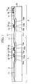
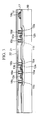
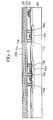
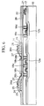
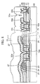
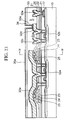
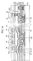
- FIGS.1 to 16 are sectional views showing a semiconductor device manufacturing method according to an embodiment of the present invention in order of the manufacturing step.
- FeRAM will be explained by way of example of the semiconductor device of the embodiment.
- a device isolation insulating film 11 is formed on a part of a surface of a p-type silicon (semiconductor) substrate 10 selectively.
- LOCOS Local Oxidation of Silicon
- Other device isolation structure forming method in addition to LOCOS, a method of STI (Shallow Trench Isolation) may be employed as the device isolation insulating film 11.
- a p-well 12a and an n-well 12b are formed by doping selectively p-type impurity and n-type impurity into predetermined active regions (transistor forming regions) of a memory cell region 1 and a peripheral circuit region 2 on the silicon substrate 10.
- a p-well (not shown) used to form CMOS is also formed in the peripheral circuit region 2.
- a silicon oxide film is formed as a gate insulating film 10a by thermally oxidising a surface of the active region of the silicon substrate 10.
- an amorphous silicon film and a tungsten silicide film are formed in sequence on the overall upper surface of the silicon substrate 10, and then the amorphous silicon film and the tungsten silicide film are patterned into predetermined shapes by the photolithography method.
- gate electrodes 13a to 13c and a wiring 14 are formed.
- a polysilicon film may be formed in place of the amorphous silicon film constituting the gate electrodes 13a to 13c.
- two gate electrodes 13a, 13b are arranged in almost parallel on one p-well 12a. These gate electrodes 13a, 13b constitute a part of the word line WL.
- n-type impurity diffusion regions 15a serving as source/drain of the n-channel MOS transistor are formed by implanting n-type impurity into the p-well 12a on both sides of the gate electrodes 13a, 13b.
- an n-type impurity diffusion region may be formed on the p-well (not shown) of the peripheral circuit region 2.
- p-type impurity diffusion regions 15b serving as source/drain of the p-channel MOS transistor are formed by implanting p-type impurity into the n-well 12b on both sides of the gate electrode 13c. The implantation of the n-type impurity and the p-type impurity is separated by using the resist pattern.
- Silicon oxide (SiO 2 ) may be formed as the insulating film by the CVD method, for example.
- a silicon oxide-nitride (SiON) film of about 200 nm thickness is formed as a cover film 3 on the overall surface of the silicon substrate 10 by the plasma enhanced CVD method.
- the silicon oxide (SiO 2 ) of about 1.0 ⁇ m thickness is grown on the cover film 3 by the plasma enhanced CVD method using a TEOS gas, whereby a first interlayer insulating film 17 is formed.
- the SiO 2 film that is formed by the plasma enhanced CVD method using the TEOS gas is also referred to as a TEOS film hereinafter.
- the densifying process of the first interlayer insulating film 17 such first interlayer insulating film 17 is annealed at the temperature of 700 °C for 30 minutes in the nitrogen atmosphere at the atmospheric pressure. Then, an upper surface of the first interlayer insulating film 17 is planarized by polishing the first interlayer insulating film 17 by using the CMP (Chemical Mechanical Polishing) method.
- CMP Chemical Mechanical Polishing
- contact holes 17a to 17d whose depth reaches the impurity diffusion regions 15a, 15b and a via hole whose depth reaches the wiring 14 are formed in the first interlayer insulating film 17 by the photolithography method respectively.
- a Ti (titanium) thin film of 20 nm thickness and a TiN (titanium nitride) thin film of 50 nm thickness are formed in sequence on the first interlayer insulating film 17 and in the holes 17a to 17e by the sputter method.
- W tungsten
- the tungsten film is buried in the contact holes 17a to 17d and the via hole 17e.
- the tungsten film, the TiN thin film, and the Ti thin film are polished by the CMP method until the upper surface of the first interlayer insulating film 17 is exposed.
- the tungsten film, etc. remained in the holes 17a to 17e after this polishing are used as plugs 18a to 18e that are used to electrically connect a wiring (interconnection) described later to the impurity diffusion regions 15a, 15b and the wiring 14.
- the first plug 18a formed on the n-type impurity diffusion region 15a, that is put between two gate electrodes 13a, 13b on one p-well 12a in the memory cell region 1, is connected to the bit line described later, and two remaining second plugs 18b are connected to the capacitor described later.
- impurity may be ion-implanted into the impurity diffusion regions 15a, 15b for the purpose of contact compensation.
- an SiON film (insulating film) 21 of 100 nm thickness is formed on the first interlayer insulating film 17 and the plugs 18a to 18e by the plasma enhanced CVD method using silane (SiH 4 ) and then an SiO 2 film 22 of 150 nm thickness is formed by the plasma enhanced CVD method using TEOS and oxygen as a reaction gas.
- This SiON film 21 is formed to prevent the penetration of the moisture into the first interlayer insulating film 17.
- these films are annealed at the temperature of 650 °C for 30 minutes in the nitrogen atmosphere at the atmospheric pressure.
- the first interlayer insulating film 17 and the SiO 2 film 22, that are formed by the plasma enhanced CVD method using the TEOS gas, are annealed at the temperatures of 700 °C and 650 °C respectively.
- the metal film such as the aluminum film with a low melting point does not exit below these films, the annealing of these films to such extent exerts no bad influence upon the underlying film.
- a first conductive film 23a having a double-layered structure is formed on the SiO 2 film 22 by depositing Ti and Pt (platinum) in sequence with the use of the DC (Direct Current) sputter method.
- a thickness of the Ti film is set to about 10 to 30 nm
- a thickness of the Pt film is set to about 100 to 300 nm.
- a thickness of the Ti film is set to 20 nm
- a thickness of the Pt film is set to 175 nm.
- a film made of iridium, ruthenium, ruthenium oxide, iridium oxide, strontium ruthenium oxide (SrRuO 3 ), or the like may be formed as the first conductive film 23a.
- a PZT film 24a of 100 to 300 nm thickness is formed on the first conductive film 23a by depositing lead zirconate titanate (PZT: Pb(Zr 1 - x Ti x )O 3 ) as the ferroelectric material by using the RF (Radio Frequency) sputter method.
- PZT lead zirconate titanate
- RF Radio Frequency
- the RTA Rapid Thermal Annealing
- the PZT film 24a is annealed at the temperature of 750 °C for 60 seconds.
- the method of forming the ferroelectric film there are the spin-on method, the sol-gel process, the MOD (Metal Organic Deposition) method, and the MOCVD method in addition to the above sputter method.
- the ferroelectric material there are lanthanum lead zirconate titanate (PLZT), SrBi 2 (Ta x Nb 1-x ) 2 O 9 (where 0 ⁇ x ⁇ 1), Bi 4 Ti 2 O 12 , etc. in addition to PZT.
- the high-dielectric material such as (BaSr)TiO 3 (BST), strontium titanate (STO), etc. may be used in place of the above ferroelectric material.
- a Pt film of 100 to 300 nm thickness is formed as a second conductive film 25a on the PZT film 24a by the DC sputter method.
- a thickness of the second conductive film 25a is set to 200 nm.
- an iridium oxide (IrO 2 ) film or ruthenium strontium oxide (SRO) may be formed by the sputter method.
- a capacitor Q having a predetermined shape is formed by patterning the second conductive film 25a, the PZT film 24a, and the first conductive film 23a in sequence by virtue of the photolithography method.
- the second conductive film 25a serves as an upper electrode 25
- the PZT film 24a serves as a dielectric film 24
- the first conductive film 23a serves as a lower electrode 23.
- the capacitor Q is formed of the upper electrode 25, the electric film 24, and the lower electrode 23.
- the capacitors Q of the same number as the MOS transistors formed in one p-well 12a are formed around the p-well 12a.
- the recovery annealing is applied to remove the damage of the capacitor Q. More particularly, after the silicon substrate 10 is placed in the oxygen atmosphere, the capacitor Q is annealed at the temperature of 500 to 700 °C for 30 to 120 minutes. For example, the recovery annealing is applied by heating at the temperature of 650 °C for 60 minutes. Also, after the lower electrode 23 is formed by patterning the first conductive film 23a, the recovery annealing is applied under the same conditions.
- a second interlayer insulating film 26 having a double-layered structure consisting of the TEOS film and the SOG (Spin-On-Glass) film is formed on the overall surface such that the capacitor Q is covered by the second interlayer insulating film 26.
- the TEOS film of 100 to 300 nm thickness is formed on the overall upper surface of the silicon substrate 10 by the plasma enhanced CVD method using the TEOS gas at the growth temperature of 390 °C and the electric power of 400 W.
- the SOG film is forced by coating an SCG solution on the TEOS film to have a thickness of 80 to 200 nm and then heating the SOG solution.
- a thickness of the TEOS film is set to 200 nm and a thickness of the SOG film is set to 100 nm.
- the SOG film is a coating insulating film, surface unevenness of the SOG film becomes small.
- the SOG film may be removed.
- the thickness of the SOG film is 100 nm
- the thickness of the TEOS film is 500 nm.
- a contact hole 26a is formed on the upper electrode 25 of the capacitor Q by patterning the second interlayer insulating film 26 by virtue of the photolithography method.
- the recovery annealing is applied the dielectric film 24. More particularly, the capacitor Q is annealed in the oxygen atmosphere at the temperature of 500 to 650 °C for 30 to 120 minutes. In this example, the recovery annealing is applied by heating at the temperature of 550 °C for 60 minutes.
- a contact hole 26b is formed on the second plug 18b in the memory cell region 1 by patterning the second interlayer insulating film 26, the SiON film 21, and the SiO 2 film 22 by virtue of the photolithography method to expose the second plug 18b.
- a TiN film of 100 nm thickness is formed on the second interlayer insulating film 26 and in the contact holes 26a, 26b by the sputter method.
- a local interconnection 27 that is used to connect electrically the second plug 18b on the p-well 12a and the upper electrode 23 of the capacitor via the contact holes 26a, 26b in the memory cell region 1 is formed by patterning the TiN film by virtue of the photolithography method.
- the TEOS film of 200 to 400 nm, e.g., 300 nm thickness is formed on the local interconnection 27 and the second interlayer insulating film 26 by the plasma enhanced CVD method.
- This TEOS film is used as a third interlayer insulating film 31.
- the unevenness of the upper surface of the third interlayer insulating film 31 is not large to need the polishing, owing to the unevenness of the upper surface of the underlying second interlayer insulating film 26.
- a contact hole 31a is formed on the first plug 18a positioned in a center area of the p-well 12a in the memory cell region 1 and also contact holes 31c to 31e are formed on respective plugs 18c to 18e in the peripheral circuit region 2.
- a Ti film, a TiN film, an Al (aluminum) film, and a TiN film are stacked in sequence on the third interlayer insulating film 31 and in the contact holes 31c to 31e to constitute four layers. If these metal films are patterned, a bit line 32a is formed in the memory cell region 1 and also wirings 32c to 32e are formed in the peripheral circuit region 2. The bit line 32a and the wirings 32c to 32e act as the first-layer aluminum wiring (interconnection).
- the bit line 32a in the memory cell region 1 is connected to the first plug 18a, and the wirings 32c to 32e in the peripheral circuit region 2 are connected to the plugs 18c to 18e.
- a thickness of the Ti film as the lowest layer is set to 20 nm
- a thickness of the underlying TiN film is set to 50 nm
- a thickness of the Al film is set to 500 nm
- a thickness of the overlying TiN film is set to 100 nm.
- a fourth interlayer insulating film 33 that is formed of SiO 2 and has a thickness of 2.0 ⁇ m is formed on the third interlayer insulating film 31, the bit line 32a, and the wirings 32c to 32e by the plasma enhanced CVD method using the TEOS gas and the oxygen (O 2 ) gas.
- the plasma CVD equipment includes a chamber in which a first electrode for loading the silicon substrate 10 thereon and a second electrode opposed to the first electrode are arranged, and a single frequency applying structure which applies a high frequency power to the second electrode and keeps the first electrode at a constant voltage.
- the growth temperature is less than 400 °C, e.g., 390 °C, and the pressure is set to 1.2 Pa.
- the frequency of the high frequency power is 13.56 MHz, and the power is set to 400 W.
- a flow rate ratio of the oxygen to the TEOS gas is set to about 1, for example. According to these conditions, the ferroelectric material constituting the capacitor Q is hardly degraded during film formation and the bit line 32a and the wirings 32c to 32e are not affected badly.
- the fourth interlayer insulating film 33 that is formed by the plasma enhanced CVD method using the TEOS gas and the oxygen gas is grown isotropically, the upper surface shape of the fourth interlayer insulating film 33 is easily affected by the shape the underlying first-layer aluminum wiring such as the bit line 32a, the wirings 32c to 32e, etc. Accordingly, when the second-layer aluminum wiring is to be formed on the TEOS film serving as the bit line 32a and the wirings 32c to 32e, such problems are caused that patterning precision of the second-layer aluminum wiring is deteriorated, the disconnection of the wiring easily occurs, etc.
- the step of polishing the upper surface by the CMP method may be employed.
- An amount of polishing is set to an about 1.0 ⁇ m in thickness from the uppermost surface.
- the ferroelectric material constituting the dielectric film 24 of the capacitor is reduced by the moisture in the interlayer insulating film to loss the ferroelectric property, or interfaces between the ferroelectric material and the electrodes are degraded by the moisture.
- the fourth interlayer insulating film 33 and the third interlayers insulating film 31 are annealed in the situation that the fourth interlayer insulating film 33 is covered with a metal film described later, the moisture absorbed in the fourth interlayer insulating film 33 becomes hard to be discharged to the outside.
- the moisture penetrates into the third interlayer insulating film 31 through a clearance between the bit wirings 32a to reach the periphery of the capacitor Q, so that degradation of the capacitor Q due to the moisture is accelerated.
- the dehydration process is applied to the fourth interlayer insulating film 33 by the plasma annealing.
- the silicon substrate 10 is loaded in the chamber of the plasma generation equipment (not shown), then an N 2 O gas and an N 2 gas are supplied into the chamber at flow rates of 700 scan and 200 scan respectively and are plasmanized, and then the fourth interlayer insulating film 33 is exposed to the plasma at the substrate temperature of less than 450°C, e.g., 350 °C, for three minutes, preferably more than four minutes. Accordingly, the moisture in the fourth interlayer insulating film 33 is discharged to the outside, and SiON is formed in at least the surface of the fourth interlayer insulating film 33 by introducing nitrogen and thus the moisture is hard to enter there into after this.
- the nitrogenizing temperature is required more than 1000 °C. Because, the N 2 is inactive, when more active gas than N 2 gas, for example, ammonia (NH 3 ) gas, is employed to nitrogenize the plasma TEOS, the heating temperature is required more than 750 °C . Such temperature melts the aluminium wiring under the plasma TEOS film.
- N 2 is inactive, when more active gas than N 2 gas, for example, ammonia (NH 3 ) gas, is employed to nitrogenize the plasma TEOS, the heating temperature is required more than 750 °C . Such temperature melts the aluminium wiring under the plasma TEOS film.
- NH 3 ammonia
- the plasma annealing is most effective nitrogenizing of the plasma TEOS film.
- the plasma annealing is performed at the temperature of less than 450 °C, such annealing never affects adversely the first-layer aluminum wirings 32a, 32c to 32e formed below the fourth interlayer insulating film 33.
- the plasma annealing is applied to the fourth interlayer insulating film 33.
- the N 2 O plasma annealing is effective to remove the moisture that enters in the polishing process.
- it becomes apparent that good characteristics of the dielectric or high-dielectric capacitor Q can be maintained via the plasma annealing under the above conditions.
- the TEOS film as a redeposited interlayer insulating film 34 is formed on the fourth interlayer insulating film 33 to have a thickness of more than 100 nm, e.g., 200 nm.
- the redeposited interlayer insulating film 34 is formed to cover cavities that appear on the polished surface of the fourth interlayer insulating film 33.
- the redeposited interlayer insulating film 34 acts as a cap layer and also has an advantage to prevent the moisture reabsorption of the fourth interlayer insulating film 33. An optimum film thickness of the redeposited interlayer insulating film 34 will be described later.
- the N 2 O plasma annealing may be applied to the redeposited interlayer insulating film 34.
- the TEOS film is formed by the plasma enhanced CVD method, such TEOS film is grown isotropically. Then, the film thickness becomes about 2.0 ⁇ m, the cavities are ready to generate between the first-layer aluminum wirings, i.e. between the bit lines 32a in the memory cell region 1 and the first-layer aluminum wirings 32c to 32e in the peripheral circuit region 2.
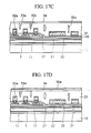
- FIG.17A is a sectional view showing a sactional shape taken along a I-I line in FIG.8, and FIG.17B is a sectional view showing a sectional shape taken along a II-II line in FIG.9.
- references 32f, 32g denotes the first-layer aluminum wiring respectively.
- the cavities 33u exposed from the fourth interlayer insulating film 33 in the memory cell region 1 appear like a slit along the bit lines 32a between them. Therefore, if a wiring forming metal film is directly formed on the fourth interlayer insulating film 33 in the situation that the cavities 33u are exposed, the metal film is filled into the cavities. Thus, after the wiring is formed by patterning the metal film, the metal film in the cavities 33u is not removed and be still left. Since the metal film in the cavities 33u acts as the medium that short-circuits the mutual wirings formed of the same metal film, it is necessary not to form previously the metal film in the cavities 33u.
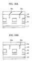
- FIG.18A is a sectional view showing the fourth interlayer insulating film 33 and an underlying structure if no redeposited interlayer insulating film 34 is provided
- FIG.18B is a sectional view showing the state that the redeposited interlayer insulating film 34 is formed on the fourth interlayer insulating film 33.
- FIGS.18A and 18B are illustrated based on a sectional microphotographs of the memory cell region of the FeRAM.
- the process is advanced to the step of forming the second-layer aluminum wiring, as shown in FIG.12 to FIG.16.
- a via hole 33a that reaches the first-layer aluminum wiring, e.g., the wiring 32d in the peripheral circuit region 2 is formed by patterning the redeposited interlayer insulating film 34 and the fourth interlayer insulating film 33 by using the photolithography method. After this, the surface of the wiring 32d formed under the fourth interlayer insulating film 33 is etched by a predetermined depth, e.g. a depth of 35 nm, through the via hole 33a.
- FIG.17D is a sectional view showing a sectional shape taken along a IV-IV line in FIG.13.
- tungsten seed (not shown) is formed on the glue layer 35a by the CVD method using a tungsten hexafluoride (WF 6 ) gas and a silane (SiH 4 ) gas.
- a tungsten film 35b is formed on the glue layer 35a at the growth temperature of 430 °C by adding a hydrogen (H 2 ) gas to the WF 6 gas and the silane (SiH 4 ) gas.
- H 2 hydrogen
- FIG.15 shows the case where the glue layer 35a is removed from the upper surface of the redeposited interlayer insulating film 34 by the CMP method.
- a via (plug) 35 that electrically connects the wiring 32 to the overlying wiring 36 is formed in the via hole 33a.
- a width of the cavity 33u appeared from the polished surface of the fourth interlayer insulating film 33 is not uniform because of variaton in polishing by the CMP method and so on. If the exposed width of the cavity 33u is varied, following problems are caused. That is, as shown in FIG.19A, when the thin redeposited interlayer insulating film 34 is formed on the cavities 33u exposed from the fourth interlayer insulating film 33, the cavities 33u are not completely covered with the redeposited interlayer insulating film 34 and a part of them is still exposed, as shown in FIG.19B. Then, as shown in FIG.19C, if the above glue layer 35a is formed under such condition, there is a possibility that such glue layer 35a is disconnected on the cavities 33u to form slits.
- hydrogen in the reaction gas employed in forming the tungsten film 35b enters into the fourth interlayer insulating film 33 via the slits, as shown in FIG.19D.
- the hydrogen penetrated into the fourth interlayer insulating film 33 is not preferable since it reduces the capacitor Q to degrade the capacitor characteristic.
- FIG.20 An ordinate of FIG.20 denotes a leakage occurring frequency between the wirings and an abscissa denotes a leakage current value.
- the film thickness of the redeposited interlayer insulating film 34 is 50 nm, the leakage occurring frequency between the wirings is large and then leakage occurring frequency between the wirings is reduced as the film thickness is increased, and the short-circuit between the wirings can be substantially prevented at the film thickness of 100 nm. Accordingly, it is desired that, in order to reduce the leakage between the wirings because of the exposure of the cavities 33u, the film thickness of the redeposited interlayer insulating film 34 should be set to at least 100 nm.
- Thickness of Second interlayer Insulating film polarization charge amount after process out after baking 0 nm 24.2 ⁇ C/cm 2 11.4 ⁇ C/cm 2 100 nm 25.1 ⁇ C/cm 2 17.5 ⁇ C/cm 2 300 nm 25.3 ⁇ C/cm 2 22.6 ⁇ C/cm 2
- the polarization charge amount is slightly larger if the redeposited interlayer insulating film is formed thicker. In contrast, after annealing, difference of the polarization charge amount between samples becomes remarkable. Especially, if the film thickness of the redeposited interlayer insulating film 34 is 0 nm, i.e., if the redeposited interlayer insulating film 34 is not formed, the polarization charge amount is reduced to the half or less after the annealing and the characteristic of the ferroelectric capacitor Q is considerably degraded. In addition, if the film thickness of the redeposited interlayer insulating film 34 is 300 nm, degradation of the ferroelectric capacitor Q is slight. Thus, the polarization charge amount after the annealing is reduced to 22.6 ⁇ C/cm 2 , which is a sufficient value to operate the FeRAM normally.
- the film thickness of the redeposited interlayer insulating film 34 such as 300 nm is decided with regard to the variation of the exposed portion of the cavities 33u.
- the redeposited interlayer insulating film 34 is formed excessively thick, an aspect ratio of the via hole 33a is increased, so that coverage of the glue layer 35a and the tungsten film 35b in the via hole 33a becomes worse. That is, the upper limit value of the film thickness of the redeposited interlayer insulating film 34 is decided based on the aspect ratio of the via hole 33a. For example, in the event that the aspect ratio of the via hole 33a is set to 2.3, the redeposited interlayer insulating film 34 needs the film thickness of about 0.4 ⁇ m (400 nm) if a diameter of the via hole 33a is set to 0.6 11 ⁇ m and the thickness of the fourth interlayer insulating film 33 is set to 1.0 ⁇ m.
- a wiring 36 is formed by forming a 50 nm thick first TiN film, a 500 nm Al film, and a 50 nm thick second TiN film in sequence on the redeposited interlayer insulating film 34 and then patterning these films. If the glue layer 35a is left on the upper surface of the redeposited interlayer insulating film 34, formation of the first TiN film is omitted and thus the aluminum film and thus the second TiN film are formed on the glue layer 35a.
- a second-layer aluminum wiring 36 is formed on the redeposited interlayer insulating film 34 by patterning the first and second TiN films and the Al film or the second TiN film, the Al film, and the glue layer by means of the photolithography method.
- an SiO 2 film of 200 nm thickness is formed as a first cover insulating film 37 on the second-layer aluminum wiring 36 and the redeposited interlayer insulating film 34 by the plasma enhanced CVD method using TEOS.
- a second cover insulating film 38 made of SiN and having a thickness of 500 nm is formed on the first cover insulating film 37 by the plasma enhanced CVD method.
- the second-layer wiring 36 is covered with the first cover insulating film 37 and the second cover insulating film 38.
- FIG.21 Planar positional relationships between various conductive patterns in the memory cell region 1 after the second-layer wiring 36 is formed are shown in FIG.21. In this case, insulating films except the device isolation insulating film 11 are omitted from FIG.21.
- the upper surface of the fourth interlayer insulating film 33 covering the capacitor Q and the first-layer aluminum wiring 32a is planarized by the CMP method. Accordingly, pattern precision of the second-layer aluminum wiring 36 that is formed flat on the fourth interlayer insulating film 33 formed on the capacitor Q and the wiring 32a can be improved.
- the moisture in the fourth interlayer insulating film 33 is removed by applying the N 2 O plasma annealing after the fourth interlayer insulating film 33 is polished, reduction and degradation of the ferroelectric film (capacitor dielectric film 24) can be avoided even when the heating is applied by succeeding steps. As a result, the FeRAM having the good characteristics can be manufactured.
- the N 2 O plasma annealing is carried out at the temperature of less than 450 °C, the first-layer aluminum wiring is never degraded.
- the polarization charge amount of the capacitor Q is axamined in both cases that the FeRAM is formed by applying the N 2 O plasma annealing step and the FeRAM is formed by omitting such N 2 O plasma annealing step. Then, the results shown in Table 2 are derived. It has been confirmed that the N 2 O plasma annealing is effective to prevent the degradation of the capacitor.
- the gas used in the dehydration process is not limited to the N 2 O gas.
- the same advantage can be achieved by the plasma annealing employing a single gas such as an N 2 gas or an O 2 gas or an NO gas or a mixed gas such as N 2 O + N 2 , or N 2 O +O 2 .
- the inert gas such as Ar, He, or Ne may be mixed with the single gas or the mixed gas.
- the redeposited interlayer insulating film 34 is formed after the dehydration process is applied to the fourth interlayer insulating film 33.
- the redeposited interlayer insulating film 34 is formed on the fourth interlayer insulating film 33 which has been subjected to the CMP polishing and then the dehydration process may be applied.
- the redeposited interlayer insulating film 34 is formed thin like the above embodiment, an amount of moisture contained in the redeposited interlayer insulating film 34 is very small. In contrast, if the redeposited interlayer insulating film 34 is formed thick, there is a possibility that the capacitor dielectric film is reduced by the moisture contained in the redeposited interlayer insulating film 34. In order to prevent this, after the redeposited interlayer insulating film 34 is formed, the dehydration process may applied by the plasma annealing using N 2 O or NO.
- the redeposited interlayer insulating film 34 is formed of the silicon oxide nitride (SiON) film by the plasma enhanced CVD method or the silicon nitride (SiN) film by the plasma enhanced CVD method, the moisture in the fourth interlayer insulating film 33 cannot be sufficiently removed since these films are hard to penetrate. Therefore, it is preferable that, if the plasma annealing is applied after the redeposited interlayer insulating film 34 is formed, the redeposited interlayer insulating film 34 should be formed of the plasma TEOS film, the O 3 -TEOS film, or the plasma SiO 2 film.
- the TEOS (O 3 -TEOS) film formed by the thermal CVD method using O 3 and TEOS, the SiO 2 (P-SiO 2 ) film formed by the plasma enhanced CVD method, the SiO 2 film formed by the non-bias HDP (High Density Plasma)-CVD, the SiON (P-SiON) film formed by the plasma enhanced CVD method, the SiN (P-SiN) film formed by the plasma enhanced CVD method, etc. may be employed as the redeposited interlayer insulating film 34.
- the P-TEOS film is employed in the above steps.
- the SiON film and the SiN film have low moisture permeability, if these films are used as the redeposited interlayer insulating film 34, the redeposited interlayer insulating film 34 must be formed after the dehydration process of the fourth interlayer insulating film 33 is performed.
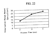
- FIG.22 is a graph showing a dependency of the polarization charge amount on a dehydration process time, wherein an abscissa denotes the plasma annealing process time of the interlayer insulating film and an ordinate denotes the polarization charge amount (QSW).
- the temperature is 350 °C
- the plasma applied power is 300 W
- a flow rate of N 2 O is 700 seem
- a flow rate of the N 2 gas is 200 seem. It is possible to say that, if a value of the polarization charge amount QSW is increased, the polarization characteristic can be improved.
- the sufficient characteristic can be obtained by setting the plasma annealing process time to three minutes or more.
- the polarization charge amount of the ferroelectric film in the initial state is about 28 ⁇ C/cm 2 .
- the polarization charge amount can be recovered up to the initial state by executing the plasma annealing for four minutes.
- the SiO 2 film formed by the plasma enhanced CVD method using the TEOS gas is employed as the fourth interlayer insulating film 33.
- the fourth interlayer insulating film 33 may be formed by the TEOS (O 3 -TEOS) film formed by the thermal CVD method using O 3 and TEOS, the SiO 2 (P-SiO 2 ) film formed by the plasma enhanced CVD method, etc.
- the growth rate of the O 3 TEOS film is smaller than that of the P-TEOS film. And, it is hard to form a cavity in the O 3 -TEOS film.
- the FeRAM and steps of forming the same are explained. Also, in the volatile memory having the high-dielectric capacitor (DRAM), insulating property of the high-dielectric material is deteriorated by the moisture and the annealing, and the interface between the high-dielectric material film and the electrode is ready to degrade. Therefore, like the above, after the upper surface of the insulating film formed on the ferroelectric capacitor is planarized by the CMP method, the dehydration process of the insulating film is performed by using the gas such as N 2 O, NO, etc., otherwise the redeposited interlayer insulating film may be formed on the surface planarized after the dehydration process or before the dehydration process by using P-TEOS.
- the high-dielectric material such as (BaSr)TiO 3 , etc. may be employed as the high-dielectric material.
- an embodiment of the present invention may be applied to the fabrication of the hybrid system LSI which consists of the ferroelectric nonvolatile semiconductor memory or the high-dielectric semiconductor memory and the logic device.
- the wiring formed on the capacitor and the wiring formed on the capacitor is planarized by polishing, the wiring can be easily formed with good precision on the flat surface of the insulating film.
- the hydration process is applied to the polished insulating film by the plasma annealing containing N 2 O or NO, the moisture attached to the surface of the insulating film or the moisture penetrated into the insulating film can be more surely removed and thus reduction of the ferroelectric material or the high-dielectric material constituting the capacitor can be prevented. As a result, the degradation of the dielectric characteristic of the ferroelectric material or the high-dielectric material can be avoided, and thus the FeRAM or DRAM having the good characteristic can be manufactured.
Landscapes
- Semiconductor Memories (AREA)
- Internal Circuitry In Semiconductor Integrated Circuit Devices (AREA)
Abstract
Description
- The present invention relates to a semiconductor device and a method of manufacturing the same and, more particularly, a semiconductor device represented by a nonvolatile semiconductor memory (FeRAM: Ferroelectric Random Access Memory) using ferroelectric material for a dielectric film of a capacitor, or a volatile semiconductor memory (DRAM: Dynamic Random Access Memory) using high-dielectric material for the dielectric film of the capacitor, or a hybrid system LSI consisting of such memory device and a logic device, and a method of manufacturing the same.
- In recent years, FeRAM , which uses ferroelectric material for the dielectric film of the capacitor, has become the focus of public attention as a nonvolatile semiconductor memory with low power consumption. Also, in recent years, miniaturization and higher integration of the semiconductor memory have been demanded. In order to satisfy such demand, DRAM that uses high-dielectric material for the dielectric film of the capacitor has been developed.
- Normally, metal oxides are used as the ferroelectric material of FeRAM and the high-dielectric material of DRAM respectively.
- Such ferroelectric material and high-dielectric material are weak in a reducing atmosphere. Ferroelectric material, especially, has such a property that the polarization characteristic is readily degraded.
- In Patent Application Publication (KOKAI) Hei 9-307074, as a method of preventing the degradation in the polarization characteristic of the ferroelectric material, it is set forth that reduction of the dielectric film of the capacitor can be prevented if an underlying insulating film formed of sputter silicon oxide or SOG (Spin-On-Glass) is formed on the capacitor and then an overlying insulating film formed of silicon oxide is formed on the underlying insulating film by using ozone and TEOS (tetraethoxysilane: Si(OC2H5)4). Also, in Patent Application Publication (KOKAI) Hei 10-275897, it is set forth that the degradation in the polarization characteristic of the capacitor formed below the wiring conductive film can be prevented if the wiring conductive film is not formed in the reducing atmosphere by using the metal CVD (Chemical Vapor Deposition) equipment or the MO (Metal Organic) CVD equipment, but formed by the DC sputter. In this Publication, it is also set forth that the SiO2 film is formed on the capacitor by the plasma enhanced CVD method using TEOS and then the wiring is connected the upper electrode of the capacitor via the hole formed in the SiO2 film.
- In addition, in Patent Application Publication (KOKAI) Hei 11-238855, such a structure is set forth that the thin conductive pattern (wiring) is connected the upper electrode of the capacitor via the hole formed in the thin insulating film covering the capacitor, then the thick aluminum wiring pattern is formed on the insulating film covering the conductive pattern, and then the insulating film is formed to cover the aluminum wiring pattern.
- However, in Patent Application Publication (KOKAI) Hei 11-238855, since the film thickness of the aluminum wiring pattern used as the bit line is thick, the level of surface unevenness of the interlayer insulating film formed on the wiring pattern is increased.
- Then, if the unevenness of the interlayer insulating film covering the aluminum wiring pattern is increased, the focus of the exposure light is ready to be defocused in the photolithography step applied to form the upper wiring on the interlayer insulating film. Thus, the problem that patterning precision of the upper wiring is lowered is caused. In particular, if the interlayer insulating film is formed by the plasma enhanced CVD method, the level of the surface unevenness of the interlayer insulating film is ready to increase.
- In contrast, it is possible to consider that the HDP (High Density Plasma) CVD SiO2 film which has small surface unevenness may be formed. In this case, there is a possibility that hydrogen attacks into the insulating film in forming the HDP CVD SiO2 film to thus reduce the oxide dielectric film of the capacitor
- It is therefore desirable to provide a semiconductor device capable of forming the wiring, that is formed over the capacitor using ferroelectric material or high-dielectric material and the bit line, with good precision and also preventing degradation of the capacitor, and a method of manufacturing the same.
- According to an embodiment of one aspect of the present invention, there is provided a semiconductor device which comprises the capacitor using the ferroelectric material or the high-dielectric material, the first wiring formed on the capacitor via the insulating film, the insulating film which is formed on the first wiring and whose upper surface is planarized, and the second wiring formed on the insulating film.
- Therefore, the pattern of the second wiring formed over the capacitor using the ferroelectric material or the high-dielectric material can be formed with good precision.
- According to an embodiment of another aspect of the present invention, there is provided a method of manufacturing a semiconductor device which includes the steps of forming the first insulating film over the capacitor after the capacitor using the ferroelectric material or the high-dielectric material as the dielectric film is formed, and then planarizing the first insulating film by the CMP (Chemical Mechanical Polishing) method, for example.
- In the polishing step, not only does the moisture in the abrasive agent or the moisture in the cleaning solution become attached to the surface of the first insulating film, but the moisture also enters into the first insulating film. In an embodiment of the present invention, in order to remove the moisture attached to the surface of the first insulating film and to prevent the moisture entering into the first insulating film, the dehydration process is applied to the polished surface of the first insulating film by the plasma annealing in the plasma atmosphere of the N2O gas or the NO gas, for example.
- Incidentally, if the moisture in/on the insulating film is removed in the electric furnace, the heating temperature in the electric furnace is limited to under 450 °C to prevent the metal wiring, for example, aluminum wiring, under the insulating film from deteriorating. However, annealing at such a low temperature is incapable of causing dehydration. In an embodiment of the present invention, plasma annealing is capable of removing the moisture in/on the insulating film under 450 °C. And, it is hard to oxidise the metal wiring under the insulating layer in the low temperature of under 450 °C.
- The moisture in the first insulating film can be removed more surely by the plasma annealing rather than the simple thermal process. Therefore, reduction of the ferroelectric film or the high-dielectric film and degradation of the capacitor due to the moisture on the surface of the first insulating film or in the first insulating film can be prevented, and thus good quality FeRAM or DRAM can be manufactured.
- When the first insulating film is formed of silicon oxide, at least the surface of the first insulating film includes nitrogen after the plasma annealing used N2O or N2.
- When the cavities (blowholes, voids or key holes) are formed in the first insulating film whose surface is planarized by the CMP method, the cavities are exposed from the polished surface like slits in some cases. Then, if the wiring layer is formed on the polished surface, there is a possibility that, because the conductive material constituting the wiring layer is filled into the cavities, a plurality of wwirings crossing the cavities are short-circuited. For this reason, it is preferable that the second insulating film should be formed on the polished surface of the first insulating film to cover or fill the cavities exposed from the polished surface of the first insulating film.
- In order to achieve the above advantage reliably, it is preferable that the thickness of the second insulating film is set to 100 nm or more.
- If the cavities not being covered with the second insulating film is produced partially since the width of the cavities exposed from the polished surface is varied, there is a possibility that slits are formed on a part of slits in the metal film formed on the second insulating film. If the slits exit on the metal film, the capacitor is degraded in some cases because the hydrogen enters into the first insulating film via the slits. Therefore, it is preferable that, in order to prevent generation of the slits on the metal film, the film thickness of the second insulating film should be set to at least 300 nm.
- In addition, the second insulating film is first formed on the first insulating film and then the above plasma annealing may be applied. In this case, not only can the degradation of the first and second insulating films be avoided, but also the moisture contained in the first and second insulating films can be removed simultaneously.
- Reference will now be made, by way of example, to the accompanying drawings, in which:
- FIGS.1 to 16 are sectional views showing a semiconductor device manufacturing method according to an embodiment of the present invention;
- FIG.17A is a sectional view showing a sectional shape taken along a I-I line in FIG.8, and FIG.17B is a sectional view showing a sectional shape taken along a II-II line in FIG.9, and FIG.17C is a sectional view showing a sectional shape taken along a III-III line in FIG.11, and FIG.17D is a sectional view showing a sectional shape taken along a IV-IV line in FIG.13;
- FIG.18A is a sectional view showing a sectional shape in FIG.17B depicted based on a microphotograph, and FIG.18B is a sectional view showing a sectional shape in FIG.17C depicted based on a microphotograph;
- FIGS.19A to 19D are sectional views showing steps by which cavities shown in FIG.17B are not sufficiently buried by an insulating film;
- FIG.20 is a graph showing a leakage current and a cumulative probability in a capacitor that is used in a memory cell of a semiconductor device according to the embodiment of the present invention, wherein an ordinate denoting the cumulative probability and an abscissa denoting the leakage current are plotted in a logarithmic scale;
- FIG.21 is a plane view showing arrangement of conductive patterns of a memory cell region of the semiconductor device according to the embodiment of the present invention; and
- FIG.22 is a graph showing a dependency of a polarization charge amount on a dehydration process time in the capacitor formed in the semiconductor device according to the embodiment of the present invention.
-
- Embodiments of the present invention will be explained in detail with reference to the accompanying drawings hereinafter.
- FIGS.1 to 16 are sectional views showing a semiconductor device manufacturing method according to an embodiment of the present invention in order of the manufacturing step. In this disclosure, FeRAM will be explained by way of example of the semiconductor device of the embodiment.
- First, steps required to obtain a sectional shape shown in FIG.1 will be explained hereunder.
- As shown in FIG.1, by using the LOCOS (Local Oxidation of Silicon) method, a device
isolation insulating film 11 is formed on a part of a surface of a p-type silicon (semiconductor)substrate 10 selectively. Other device isolation structure forming method in addition to LOCOS, a method of STI (Shallow Trench Isolation) may be employed as the deviceisolation insulating film 11. - After such a device
isolation insulating film 11 is formed, a p-well 12a and an n-well 12b are formed by doping selectively p-type impurity and n-type impurity into predetermined active regions (transistor forming regions) of amemory cell region 1 and aperipheral circuit region 2 on thesilicon substrate 10. Although not shown in FIG.1, a p-well (not shown) used to form CMOS is also formed in theperipheral circuit region 2. - Then, a silicon oxide film is formed as a
gate insulating film 10a by thermally oxidising a surface of the active region of thesilicon substrate 10. - Then, an amorphous silicon film and a tungsten silicide film are formed in sequence on the overall upper surface of the
silicon substrate 10, and then the amorphous silicon film and the tungsten silicide film are patterned into predetermined shapes by the photolithography method. Thus,gate electrodes 13a to 13c and awiring 14 are formed. A polysilicon film may be formed in place of the amorphous silicon film constituting thegate electrodes 13a to 13c. - In the
memory cell region 1, twogate electrodes well 12a. Thesegate electrodes - Then, in the
memory cell region 1, n-typeimpurity diffusion regions 15a serving as source/drain of the n-channel MOS transistor are formed by implanting n-type impurity into the p-well 12a on both sides of thegate electrodes peripheral circuit region 2. In turn, in theperipheral circuit region 2, p-typeimpurity diffusion regions 15b serving as source/drain of the p-channel MOS transistor are formed by implanting p-type impurity into the n-well 12b on both sides of thegate electrode 13c. The implantation of the n-type impurity and the p-type impurity is separated by using the resist pattern. - Then, an insulating film is formed on the overall surface of the
silicon substrate 10, and thensidewall insulating films 16 are formed on both sides of thegate electrodes wiring 14 by etching back the insulating film. Silicon oxide (SiO2) may be formed as the insulating film by the CVD method, for example. - Then, a silicon oxide-nitride (SiON) film of about 200 nm thickness is formed as a
cover film 3 on the overall surface of thesilicon substrate 10 by the plasma enhanced CVD method. Then, the silicon oxide (SiO2) of about 1.0 µm thickness is grown on thecover film 3 by the plasma enhanced CVD method using a TEOS gas, whereby a firstinterlayer insulating film 17 is formed. In this case, the SiO2 film that is formed by the plasma enhanced CVD method using the TEOS gas is also referred to as a TEOS film hereinafter. - Then, as the densifying process of the first
interlayer insulating film 17, such firstinterlayer insulating film 17 is annealed at the temperature of 700 °C for 30 minutes in the nitrogen atmosphere at the atmospheric pressure. Then, an upper surface of the firstinterlayer insulating film 17 is planarized by polishing the firstinterlayer insulating film 17 by using the CMP (Chemical Mechanical Polishing) method. - Next, steps required to obtain a sectional shape shown in FIG.2 will be explained hereunder.
- First,
contact holes 17a to 17d whose depth reaches theimpurity diffusion regions wiring 14 are formed in the firstinterlayer insulating film 17 by the photolithography method respectively. Then, a Ti (titanium) thin film of 20 nm thickness and a TiN (titanium nitride) thin film of 50 nm thickness are formed in sequence on the firstinterlayer insulating film 17 and in theholes 17a to 17e by the sputter method. Then, W (tungsten) is grown on the TiN thin film by the CVD method. As a result, the tungsten film is buried in the contact holes 17a to 17d and the viahole 17e. - Then, the tungsten film, the TiN thin film, and the Ti thin film are polished by the CMP method until the upper surface of the first
interlayer insulating film 17 is exposed. The tungsten film, etc. remained in theholes 17a to 17e after this polishing are used asplugs 18a to 18e that are used to electrically connect a wiring (interconnection) described later to theimpurity diffusion regions wiring 14. - The
first plug 18a formed on the n-typeimpurity diffusion region 15a, that is put between twogate electrodes well 12a in thememory cell region 1, is connected to the bit line described later, and two remainingsecond plugs 18b are connected to the capacitor described later. - In this case, after the contact holes 17a to 17d and the via
hole 17e are formed, impurity may be ion-implanted into theimpurity diffusion regions - Then, as shown in FIG.3, in order to prevent the oxidation of the
plugs 18a to 18e, an SiON film (insulating film) 21 of 100 nm thickness is formed on the firstinterlayer insulating film 17 and theplugs 18a to 18e by the plasma enhanced CVD method using silane (SiH4) and then an SiO2 film 22 of 150 nm thickness is formed by the plasma enhanced CVD method using TEOS and oxygen as a reaction gas. ThisSiON film 21 is formed to prevent the penetration of the moisture into the firstinterlayer insulating film 17. - Then, in order to densify the
SiON film 21 and the SiO2 film 22, these films are annealed at the temperature of 650 °C for 30 minutes in the nitrogen atmosphere at the atmospheric pressure. - The first
interlayer insulating film 17 and the SiO2 film 22, that are formed by the plasma enhanced CVD method using the TEOS gas, are annealed at the temperatures of 700 °C and 650 °C respectively. In this case, since the metal film such as the aluminum film with a low melting point does not exit below these films, the annealing of these films to such extent exerts no bad influence upon the underlying film. - Next, as shown in FIG.4, a first
conductive film 23a having a double-layered structure is formed on the SiO2 film 22 by depositing Ti and Pt (platinum) in sequence with the use of the DC (Direct Current) sputter method. In this case, a thickness of the Ti film is set to about 10 to 30 nm, and a thickness of the Pt film is set to about 100 to 300 nm. For example, a thickness of the Ti film is set to 20 nm, and a thickness of the Pt film is set to 175 nm. A film made of iridium, ruthenium, ruthenium oxide, iridium oxide, strontium ruthenium oxide (SrRuO3), or the like may be formed as the firstconductive film 23a. - Then, a
PZT film 24a of 100 to 300 nm thickness is formed on the firstconductive film 23a by depositing lead zirconate titanate (PZT: Pb(Zr1-xTix)O3) as the ferroelectric material by using the RF (Radio Frequency) sputter method. For example, a thickness of thePZT film 24a is set to 240 nm. - Then, as the crystallizing process of the
PZT film 24a, the RTA (Rapid Thermal Annealing) of thePZT film 24a is performed at the temperature of 650 °C to 850 °C for 30 to 120 seconds in the oxygen atmosphere. For example, thePZT film 24a is annealed at the temperature of 750 °C for 60 seconds. - As the method of forming the ferroelectric film, there are the spin-on method, the sol-gel process, the MOD (Metal Organic Deposition) method, and the MOCVD method in addition to the above sputter method. Also, as the ferroelectric material, there are lanthanum lead zirconate titanate (PLZT), SrBi2 (TaxNb1-x)2O9 (where 0<x<1), Bi4Ti2O12, etc. in addition to PZT. In addition, in order to construct the DRAM, the high-dielectric material such as (BaSr)TiO3 (BST), strontium titanate (STO), etc. may be used in place of the above ferroelectric material.
- After
such PZT film 24a is formed, a Pt film of 100 to 300 nm thickness is formed as a secondconductive film 25a on thePZT film 24a by the DC sputter method. For example, a thickness of the secondconductive film 25a is set to 200 nm. As the secondconductive film 25a, an iridium oxide (IrO2) film or ruthenium strontium oxide (SRO) may be formed by the sputter method. - Then, a capacitor Q having a predetermined shape, as shown in FIG.5, is formed by patterning the second
conductive film 25a, thePZT film 24a, and the firstconductive film 23a in sequence by virtue of the photolithography method. - At this time, the second
conductive film 25a serves as anupper electrode 25, thePZT film 24a serves as adielectric film 24, and the firstconductive film 23a serves as alower electrode 23. Thus, the capacitor Q is formed of theupper electrode 25, theelectric film 24, and thelower electrode 23. Actually, the capacitors Q of the same number as the MOS transistors formed in one p-well 12a are formed around the p-well 12a. - In the meanwhile, after the
upper electrode 25 is formed by patterning the secondconductive film 25a, the recovery annealing is applied to remove the damage of the capacitor Q. More particularly, after thesilicon substrate 10 is placed in the oxygen atmosphere, the capacitor Q is annealed at the temperature of 500 to 700 °C for 30 to 120 minutes. For example, the recovery annealing is applied by heating at the temperature of 650 °C for 60 minutes. Also, after thelower electrode 23 is formed by patterning the firstconductive film 23a, the recovery annealing is applied under the same conditions. - As shown in FIG.6, after the capacitor Q is formed via steps mentioned above, a second
interlayer insulating film 26 having a double-layered structure consisting of the TEOS film and the SOG (Spin-On-Glass) film is formed on the overall surface such that the capacitor Q is covered by the secondinterlayer insulating film 26. The TEOS film of 100 to 300 nm thickness is formed on the overall upper surface of thesilicon substrate 10 by the plasma enhanced CVD method using the TEOS gas at the growth temperature of 390 °C and the electric power of 400 W. Also, the SOG film is forced by coating an SCG solution on the TEOS film to have a thickness of 80 to 200 nm and then heating the SOG solution. In this example, a thickness of the TEOS film is set to 200 nm and a thickness of the SOG film is set to 100 nm. Here, since the SOG film is a coating insulating film, surface unevenness of the SOG film becomes small. - The SOG film may be removed. In this case, the thickness of the SOG film is 100 nm, and the thickness of the TEOS film is 500 nm.
- Then, a
contact hole 26a is formed on theupper electrode 25 of the capacitor Q by patterning the secondinterlayer insulating film 26 by virtue of the photolithography method. Then, the recovery annealing is applied thedielectric film 24. More particularly, the capacitor Q is annealed in the oxygen atmosphere at the temperature of 500 to 650 °C for 30 to 120 minutes. In this example, the recovery annealing is applied by heating at the temperature of 550 °C for 60 minutes. - Then, a
contact hole 26b is formed on thesecond plug 18b in thememory cell region 1 by patterning the secondinterlayer insulating film 26, theSiON film 21, and the SiO2 film 22 by virtue of the photolithography method to expose thesecond plug 18b. Then, a TiN film of 100 nm thickness is formed on the secondinterlayer insulating film 26 and in thecontact holes local interconnection 27 that is used to connect electrically thesecond plug 18b on the p-well 12a and theupper electrode 23 of the capacitor via thecontact holes memory cell region 1 is formed by patterning the TiN film by virtue of the photolithography method. - Then, steps required to construct a sectional shape shown in FIG.7 will be explained hereunder.
- First, the TEOS film of 200 to 400 nm, e.g., 300 nm thickness is formed on the
local interconnection 27 and the secondinterlayer insulating film 26 by the plasma enhanced CVD method. This TEOS film is used as a thirdinterlayer insulating film 31. In this case, the unevenness of the upper surface of the thirdinterlayer insulating film 31 is not large to need the polishing, owing to the unevenness of the upper surface of the underlying secondinterlayer insulating film 26. - Then, if respective films from the third
interlayer insulating film 31 to theSiON film 21 are patterned by virtue of the photolithography method, acontact hole 31a is formed on thefirst plug 18a positioned in a center area of the p-well 12a in thememory cell region 1 and also contactholes 31c to 31e are formed onrespective plugs 18c to 18e in theperipheral circuit region 2. - Then, a Ti film, a TiN film, an Al (aluminum) film, and a TiN film are stacked in sequence on the third
interlayer insulating film 31 and in the contact holes 31c to 31e to constitute four layers. If these metal films are patterned, abit line 32a is formed in thememory cell region 1 and also wirings 32c to 32e are formed in theperipheral circuit region 2. Thebit line 32a and the wirings 32c to 32e act as the first-layer aluminum wiring (interconnection). - The
bit line 32a in thememory cell region 1 is connected to thefirst plug 18a, and the wirings 32c to 32e in theperipheral circuit region 2 are connected to theplugs 18c to 18e. - As respective thicknesses of metal films constituting the
bit line 32a and the wirings 32c to 32e, for example, a thickness of the Ti film as the lowest layer is set to 20 nm, a thickness of the underlying TiN film is set to 50 nm, a thickness of the Al film is set to 500 nm, and a thickness of the overlying TiN film is set to 100 nm. - Then, as shown in FIG.8, a fourth
interlayer insulating film 33 that is formed of SiO2 and has a thickness of 2.0 µm is formed on the thirdinterlayer insulating film 31, thebit line 32a, and the wirings 32c to 32e by the plasma enhanced CVD method using the TEOS gas and the oxygen (O2) gas. - The plasma CVD equipment includes a chamber in which a first electrode for loading the
silicon substrate 10 thereon and a second electrode opposed to the first electrode are arranged, and a single frequency applying structure which applies a high frequency power to the second electrode and keeps the first electrode at a constant voltage. As the film forming conditions at this time, the growth temperature is less than 400 °C, e.g., 390 °C, and the pressure is set to 1.2 Pa. Also, the frequency of the high frequency power is 13.56 MHz, and the power is set to 400 W. A flow rate ratio of the oxygen to the TEOS gas is set to about 1, for example. According to these conditions, the ferroelectric material constituting the capacitor Q is hardly degraded during film formation and thebit line 32a and the wirings 32c to 32e are not affected badly. - Meanwhile, since the fourth
interlayer insulating film 33 that is formed by the plasma enhanced CVD method using the TEOS gas and the oxygen gas is grown isotropically, the upper surface shape of the fourthinterlayer insulating film 33 is easily affected by the shape the underlying first-layer aluminum wiring such as thebit line 32a, the wirings 32c to 32e, etc. Accordingly, when the second-layer aluminum wiring is to be formed on the TEOS film serving as thebit line 32a and the wirings 32c to 32e, such problems are caused that patterning precision of the second-layer aluminum wiring is deteriorated, the disconnection of the wiring easily occurs, etc. - Therefore, as shown in FIG.9, in order to planarize the upper surface of the TEOS film as the fourth
interlayer insulating film 33, the step of polishing the upper surface by the CMP method may be employed. An amount of polishing is set to an about 1.0 µm in thickness from the uppermost surface. - By the way, it becomes apparent based on the experiment that, if the fourth
interlayer insulating film 33 is annealed as described later after the fourthinterlayer insulating film 33 has been polished by the CMP method, a polarization charge amount of the capacitor Q can be reduced by such annealing. - This is because the moisture in the slurry used in the planarization by the CMP method and the moisture in the cleaning solution used in cleaning thereafter are attached to the surface of the TEOS film as the fourth
interlayer insulating film 33 or are absorbed into the inner region of the TEOS film to reach the underlying capacitor Q, and then such moisture degrades the capacitor Q in annealing. - More particularly, it may be guessed that, since the capacitor Q is annealed at the high temperature after the polishing of the fourth
interlayer insulating film 33, the ferroelectric material constituting thedielectric film 24 of the capacitor is reduced by the moisture in the interlayer insulating film to loss the ferroelectric property, or interfaces between the ferroelectric material and the electrodes are degraded by the moisture. In particular, if the fourthinterlayer insulating film 33 and the thirdinterlayers insulating film 31 are annealed in the situation that the fourthinterlayer insulating film 33 is covered with a metal film described later, the moisture absorbed in the fourthinterlayer insulating film 33 becomes hard to be discharged to the outside. Thus, the moisture penetrates into the thirdinterlayer insulating film 31 through a clearance between the bit wirings 32a to reach the periphery of the capacitor Q, so that degradation of the capacitor Q due to the moisture is accelerated. - Therefore, as shown in FIG.10, in order to prevent the degradation of the capacitor Q by removing the moisture that enters into the fourth
interlayer insulating film 33 in polishing or the moisture that is attached to the surface, the dehydration process is applied to the fourthinterlayer insulating film 33 by the plasma annealing. - In other words, after the fourth
interlayer insulating film 33 is planarized by the CMP method, thesilicon substrate 10 is loaded in the chamber of the plasma generation equipment (not shown), then an N2O gas and an N2 gas are supplied into the chamber at flow rates of 700 scan and 200 scan respectively and are plasmanized, and then the fourthinterlayer insulating film 33 is exposed to the plasma at the substrate temperature of less than 450°C, e.g., 350 °C, for three minutes, preferably more than four minutes. Accordingly, the moisture in the fourthinterlayer insulating film 33 is discharged to the outside, and SiON is formed in at least the surface of the fourthinterlayer insulating film 33 by introducing nitrogen and thus the moisture is hard to enter there into after this. - If the plasma TEOS film is nitrogenized by heating without plasma, in N2 atmosphere, the nitrogenizing temperature is required more than 1000 °C. Because, the N2 is inactive, when more active gas than N2 gas, for example, ammonia (NH3) gas, is employed to nitrogenize the plasma TEOS, the heating temperature is required more than 750 °C . Such temperature melts the aluminium wiring under the plasma TEOS film.
- The plasma annealing is most effective nitrogenizing of the plasma TEOS film.
- Since the plasma annealing is performed at the temperature of less than 450 °C, such annealing never affects adversely the first-
layer aluminum wirings interlayer insulating film 33. - Meanwhile, in Patent Application Publication (KOKAI) Hei 10-83990 (United States Patent 6017784), it is set forth that the silicon oxide film is formed by using the TEOS gas and then hydrogen in the silicon oxide film is degassed by the N2 or N2O plasma process. This plasma process is neither applied to the polished silicon oxide film nor the silicon oxide film covering the ferroelectric capacitor.
- In contrast, in this embodiment of the present invention, after the surface of the fourth
interlayer insulating film 33 made of SiO2 formed by using The TEOS is polished, the plasma annealing is applied to the fourthinterlayer insulating film 33. In the above reference, there is no recitation to the effect that the N2O plasma annealing is effective to remove the moisture that enters in the polishing process. Also, in the embodiment of the present invention, it becomes apparent that good characteristics of the dielectric or high-dielectric capacitor Q can be maintained via the plasma annealing under the above conditions. - As shown in FIG.11, after the above plasma annealing has been finished, the TEOS film as a redeposited
interlayer insulating film 34 is formed on the fourthinterlayer insulating film 33 to have a thickness of more than 100 nm, e.g., 200 nm. As described later, the redepositedinterlayer insulating film 34 is formed to cover cavities that appear on the polished surface of the fourthinterlayer insulating film 33. The redepositedinterlayer insulating film 34 acts as a cap layer and also has an advantage to prevent the moisture reabsorption of the fourthinterlayer insulating film 33. An optimum film thickness of the redepositedinterlayer insulating film 34 will be described later. - In this case, the N2O plasma annealing may be applied to the redeposited
interlayer insulating film 34. - Then, as described above, sometimes the cavities that are called key holes or slits (also called blowholes or voids) appear on the polished surface of the fourth
interlayer insulating film 33. The reason for this will be given in the following. - If the TEOS film is formed by the plasma enhanced CVD method, such TEOS film is grown isotropically. Then, the film thickness becomes about 2.0 µm, the cavities are ready to generate between the first-layer aluminum wirings, i.e. between the
bit lines 32a in thememory cell region 1 and the first-layer aluminum wirings 32c to 32e in theperipheral circuit region 2. - In this case, as shown in FIG.17A, since the
bit lines 32a are lifted up by the capacitor Q, thecavities 33u generated between thebit lines 32a are formed at the higher location than those in other regions. - Therefore, as shown in FIG.17B, after the fourth
interlayer insulating film 33 formed of the TEOS film is polished, thebit lines 32a formed in thememory cell region 1 are easily exposed from the polished surface. - FIG.17A is a sectional view showing a sactional shape taken along a I-I line in FIG.8, and FIG.17B is a sectional view showing a sectional shape taken along a II-II line in FIG.9. In FIG.17A and FIG.17B,
references - In this manner, the
cavities 33u exposed from the fourthinterlayer insulating film 33 in thememory cell region 1 appear like a slit along thebit lines 32a between them. Therefore, if a wiring forming metal film is directly formed on the fourthinterlayer insulating film 33 in the situation that thecavities 33u are exposed, the metal film is filled into the cavities. Thus, after the wiring is formed by patterning the metal film, the metal film in thecavities 33u is not removed and be still left. Since the metal film in thecavities 33u acts as the medium that short-circuits the mutual wirings formed of the same metal film, it is necessary not to form previously the metal film in thecavities 33u. - In the present embodiment, as shown in FIG.11, since the polished surface of the fourth
interlayer insulating film 33 is covered with the redepositedinterlayer insulating film 34 after the fourthinterlayer insulating film 33 is polished, the metal film is not formed in thecavities 33u exposed from the polished surface of the fourthinterlayer insulating film 33. A sactional shape taken along a III-III line in FIG.11 is shown like FIG.17C. - FIG.18A is a sectional view showing the fourth
interlayer insulating film 33 and an underlying structure if no redeposited interlayer insulatingfilm 34 is provided, and FIG.18B is a sectional view showing the state that the redepositedinterlayer insulating film 34 is formed on the fourthinterlayer insulating film 33. In this case, FIGS.18A and 18B are illustrated based on a sectional microphotographs of the memory cell region of the FeRAM. - After the above redeposited
interlayer insulating film 34 is formed, the process is advanced to the step of forming the second-layer aluminum wiring, as shown in FIG.12 to FIG.16. - First, as shown in FIG.12, a via
hole 33a that reaches the first-layer aluminum wiring, e.g., thewiring 32d in theperipheral circuit region 2 is formed by patterning the redepositedinterlayer insulating film 34 and the fourthinterlayer insulating film 33 by using the photolithography method. After this, the surface of thewiring 32d formed under the fourthinterlayer insulating film 33 is etched by a predetermined depth, e.g. a depth of 35 nm, through the viahole 33a. - Then, as shown in FIG.13, a Ti film of 20 nm thickness and a TiN film of 50 nm thickness are formed in sequence in the via
hole 33a and on the redepositedinterlayer insulating film 34 by the sputtering. These films constitute aglue layer 35a. Here, FIG.17D is a sectional view showing a sectional shape taken along a IV-IV line in FIG.13. - Then, tungsten seed (not shown) is formed on the
glue layer 35a by the CVD method using a tungsten hexafluoride (WF6) gas and a silane (SiH4) gas. Then, atungsten film 35b is formed on theglue layer 35a at the growth temperature of 430 °C by adding a hydrogen (H2) gas to the WF6 gas and the silane (SiH4) gas. Thus, as shown in FIG.14, theglue layer 35a and thetungsten film 35b are filled in the viahole 33a. - Then, the
tungsten film 35b formed on the redepositedinterlayer insulating film 34 is removed by the CMP method or the etching-back to be left only in the viahole 33a. At this time, theglue layer 35a formed on the redepositedinterlayer insulating film 34 may be removed or left as it is. FIG.15 shows the case where theglue layer 35a is removed from the upper surface of the redepositedinterlayer insulating film 34 by the CMP method. - Accordingly, a via (plug) 35 that electrically connects the
wiring 32 to the overlyingwiring 36 is formed in the viahole 33a. - Meanwhile, a width of the
cavity 33u appeared from the polished surface of the fourthinterlayer insulating film 33 is not uniform because of variaton in polishing by the CMP method and so on. If the exposed width of thecavity 33u is varied, following problems are caused. That is, as shown in FIG.19A, when the thin redepositedinterlayer insulating film 34 is formed on thecavities 33u exposed from the fourthinterlayer insulating film 33, thecavities 33u are not completely covered with the redepositedinterlayer insulating film 34 and a part of them is still exposed, as shown in FIG.19B. Then, as shown in FIG.19C, if theabove glue layer 35a is formed under such condition, there is a possibility thatsuch glue layer 35a is disconnected on thecavities 33u to form slits. If such slits exit, hydrogen in the reaction gas employed in forming thetungsten film 35b enters into the fourthinterlayer insulating film 33 via the slits, as shown in FIG.19D. The hydrogen penetrated into the fourthinterlayer insulating film 33 is not preferable since it reduces the capacitor Q to degrade the capacitor characteristic. - Therefore, it becomes apparent from the experimental results that, in order to cover without fail the
cavities 33u exposed from the fourthinterlayer insulating film 33, the film thickness of the redepositedinterlayer insulating film 34 in excess of at least 300 nm is needed. - Then, it is examined to which extent the film thickness of the redeposited
interlayer insulating film 34 should be formed in order to prevent the situation that theglue layer 35a and thetungsten film 35b are filled into thecavities 33u. Thus, the result shown in FIG.20 is derived. An ordinate of FIG.20 denotes a leakage occurring frequency between the wirings and an abscissa denotes a leakage current value. According to the result in FIG.20, it can be understood that, if the film thickness of the redepositedinterlayer insulating film 34 is 50 nm, the leakage occurring frequency between the wirings is large and then leakage occurring frequency between the wirings is reduced as the film thickness is increased, and the short-circuit between the wirings can be substantially prevented at the film thickness of 100 nm. Accordingly, it is desired that, in order to reduce the leakage between the wirings because of the exposure of the cavities 33u, the film thickness of the redepositedinterlayer insulating film 34 should be set to at least 100 nm. - In contrast, a relationship between the film thickness of the redeposited
interlayer insulating film 34 and change in the polarization charge amount of the capacitor is examined based on the accelerated test after a series steps are finished such that theglue layer 35a and thetungsten film 35b are formed on the redepositedinterlayer insulating film 34, then theplug 35 is formed by patterning tham, the second-layer aluminum wiring described later is formed thereon, and then the second-layer aluminum wiring is covered with the insulating film. Then, the result shown in Table 1 are obtained. In this case, the accelerated test is performed by heating the substrate up to the temperature of 200 °C for one hour in the atmosphere.Thickness of Second interlayer Insulating film polarization charge amount after process out after baking 0 nm 24.2 µC/cm2 11.4 µC/cm2 100 nm 25.1 µC/cm2 17.5 µC/cm2 300 nm 25.3 µC/cm2 22.6 µC/cm2 - According to Table 1, in the state prior to the accelerated test, the polarization charge amount is slightly larger if the redeposited interlayer insulating film is formed thicker. In contrast, after annealing, difference of the polarization charge amount between samples becomes remarkable. Especially, if the film thickness of the redeposited
interlayer insulating film 34 is 0 nm, i.e., if the redepositedinterlayer insulating film 34 is not formed, the polarization charge amount is reduced to the half or less after the annealing and the characteristic of the ferroelectric capacitor Q is considerably degraded. In addition, if the film thickness of the redepositedinterlayer insulating film 34 is 300 nm, degradation of the ferroelectric capacitor Q is slight. Thus, the polarization charge amount after the annealing is reduced to 22.6 µC/cm2, which is a sufficient value to operate the FeRAM normally. - The film thickness of the redeposited
interlayer insulating film 34 such as 300 nm is decided with regard to the variation of the exposed portion of the cavities 33u. - On the contrary, if the redeposited
interlayer insulating film 34 is formed excessively thick, an aspect ratio of the viahole 33a is increased, so that coverage of theglue layer 35a and thetungsten film 35b in the viahole 33a becomes worse. That is, the upper limit value of the film thickness of the redepositedinterlayer insulating film 34 is decided based on the aspect ratio of the viahole 33a. For example, in the event that the aspect ratio of the viahole 33a is set to 2.3, the redepositedinterlayer insulating film 34 needs the film thickness of about 0.4 µm (400 nm) if a diameter of the viahole 33a is set to 0.6 11 µm and the thickness of the fourthinterlayer insulating film 33 is set to 1.0 µm. - After the steps of forming the redeposited
interlayer insulating film 34 and the via 35 according to above steps have been completed, awiring 36 is formed by forming a 50 nm thick first TiN film, a 500 nm Al film, and a 50 nm thick second TiN film in sequence on the redepositedinterlayer insulating film 34 and then patterning these films. If theglue layer 35a is left on the upper surface of the redepositedinterlayer insulating film 34, formation of the first TiN film is omitted and thus the aluminum film and thus the second TiN film are formed on theglue layer 35a. - Then, as shown in FIG.16, a second-
layer aluminum wiring 36 is formed on the redepositedinterlayer insulating film 34 by patterning the first and second TiN films and the Al film or the second TiN film, the Al film, and the glue layer by means of the photolithography method. - Then, an SiO2 film of 200 nm thickness is formed as a first
cover insulating film 37 on the second-layer aluminum wiring 36 and the redepositedinterlayer insulating film 34 by the plasma enhanced CVD method using TEOS. Then, a secondcover insulating film 38 made of SiN and having a thickness of 500 nm is formed on the firstcover insulating film 37 by the plasma enhanced CVD method. The second-layer wiring 36 is covered with the firstcover insulating film 37 and the secondcover insulating film 38. - Planar positional relationships between various conductive patterns in the
memory cell region 1 after the second-layer wiring 36 is formed are shown in FIG.21. In this case, insulating films except the deviceisolation insulating film 11 are omitted from FIG.21. - With the above steps, a basic structure of the FeRAM using the ferroelectric substance as the
capacitor dielectric film 24 can be completed. - In the present embodiment, the upper surface of the fourth
interlayer insulating film 33 covering the capacitor Q and the first-layer aluminum wiring 32a is planarized by the CMP method. Accordingly, pattern precision of the second-layer aluminum wiring 36 that is formed flat on the fourthinterlayer insulating film 33 formed on the capacitor Q and thewiring 32a can be improved. - Also, since the moisture in the fourth
interlayer insulating film 33 is removed by applying the N2O plasma annealing after the fourthinterlayer insulating film 33 is polished, reduction and degradation of the ferroelectric film (capacitor dielectric film 24) can be avoided even when the heating is applied by succeeding steps. As a result, the FeRAM having the good characteristics can be manufactured. In addition, since the N2O plasma annealing is carried out at the temperature of less than 450 °C, the first-layer aluminum wiring is never degraded. - The polarization charge amount of the capacitor Q is axamined in both cases that the FeRAM is formed by applying the N2O plasma annealing step and the FeRAM is formed by omitting such N2O plasma annealing step. Then, the results shown in Table 2 are derived. It has been confirmed that the N2O plasma annealing is effective to prevent the degradation of the capacitor.
polarization charge amount (QSW) N2O plasma annealing 21.3 µC/cm2 No N2O plasma annealing 15.4 µC/cm2 - In the above embodiment, the case is discussed where the dehydration process is applied to the fourth
interlayer insulating film 33 by the N2O plasma annealing. But, the gas used in the dehydration process is not limited to the N2O gas. For example, the same advantage can be achieved by the plasma annealing employing a single gas such as an N2 gas or an O2 gas or an NO gas or a mixed gas such as N2O + N2, or N2O +O2. The inert gas such as Ar, He, or Ne may be mixed with the single gas or the mixed gas. - Furthermore, in the above embodiment, the redeposited
interlayer insulating film 34 is formed after the dehydration process is applied to the fourthinterlayer insulating film 33. In this case, the redepositedinterlayer insulating film 34 is formed on the fourthinterlayer insulating film 33 which has been subjected to the CMP polishing and then the dehydration process may be applied. - If the redeposited
interlayer insulating film 34 is formed thin like the above embodiment, an amount of moisture contained in the redepositedinterlayer insulating film 34 is very small. In contrast, if the redepositedinterlayer insulating film 34 is formed thick, there is a possibility that the capacitor dielectric film is reduced by the moisture contained in the redepositedinterlayer insulating film 34. In order to prevent this, after the redepositedinterlayer insulating film 34 is formed, the dehydration process may applied by the plasma annealing using N2O or NO. However, in this case, if the redepositedinterlayer insulating film 34 is formed of the silicon oxide nitride (SiON) film by the plasma enhanced CVD method or the silicon nitride (SiN) film by the plasma enhanced CVD method, the moisture in the fourthinterlayer insulating film 33 cannot be sufficiently removed since these films are hard to penetrate. Therefore, it is preferable that, if the plasma annealing is applied after the redepositedinterlayer insulating film 34 is formed, the redepositedinterlayer insulating film 34 should be formed of the plasma TEOS film, the O3-TEOS film, or the plasma SiO2 film. - More particularly, in place of the TEOS film (P-TEOS film) formed by the above plasma enhanced CVD method, the TEOS (O3-TEOS) film formed by the thermal CVD method using O3 and TEOS, the SiO2 (P-SiO2) film formed by the plasma enhanced CVD method, the SiO2 film formed by the non-bias HDP (High Density Plasma)-CVD, the SiON (P-SiON) film formed by the plasma enhanced CVD method, the SiN (P-SiN) film formed by the plasma enhanced CVD method, etc. may be employed as the redeposited
interlayer insulating film 34. In this case, since a moisture containing amount of the O3-TEOS film is larger than the P-TEOS film, the P-TEOS film is employed in the above steps. However, since the SiON film and the SiN film have low moisture permeability, if these films are used as the redepositedinterlayer insulating film 34, the redepositedinterlayer insulating film 34 must be formed after the dehydration process of the fourthinterlayer insulating film 33 is performed. - FIG.22 is a graph showing a dependency of the polarization charge amount on a dehydration process time, wherein an abscissa denotes the plasma annealing process time of the interlayer insulating film and an ordinate denotes the polarization charge amount (QSW). As the plasma annealing conditions, the temperature is 350 °C , the plasma applied power is 300 W, a flow rate of N2O is 700 seem, and a flow rate of the N2 gas is 200 seem. It is possible to say that, if a value of the polarization charge amount QSW is increased, the polarization characteristic can be improved.
- As can be seen from FIG.22, the sufficient characteristic can be obtained by setting the plasma annealing process time to three minutes or more. The polarization charge amount of the ferroelectric film in the initial state is about 28 µC/cm2. Thus, the polarization charge amount can be recovered up to the initial state by executing the plasma annealing for four minutes.
- In the above embodiment, the SiO2 film formed by the plasma enhanced CVD method using the TEOS gas is employed as the fourth
interlayer insulating film 33. In addition to this, the fourthinterlayer insulating film 33 may be formed by the TEOS (O3-TEOS) film formed by the thermal CVD method using O3 and TEOS, the SiO2 (P-SiO2) film formed by the plasma enhanced CVD method, etc. The growth rate of the O3 TEOS film is smaller than that of the P-TEOS film. And, it is hard to form a cavity in the O3-TEOS film. - In the above embodiment, the FeRAM and steps of forming the same are explained. Also, in the volatile memory having the high-dielectric capacitor (DRAM), insulating property of the high-dielectric material is deteriorated by the moisture and the annealing, and the interface between the high-dielectric material film and the electrode is ready to degrade. Therefore, like the above, after the upper surface of the insulating film formed on the ferroelectric capacitor is planarized by the CMP method, the dehydration process of the insulating film is performed by using the gas such as N2O, NO, etc., otherwise the redeposited interlayer insulating film may be formed on the surface planarized after the dehydration process or before the dehydration process by using P-TEOS. The high-dielectric material such as (BaSr)TiO3, etc. may be employed as the high-dielectric material.
- Also, an embodiment of the present invention may be applied to the fabrication of the hybrid system LSI which consists of the ferroelectric nonvolatile semiconductor memory or the high-dielectric semiconductor memory and the logic device.
- As described above, according to an embodiment of the present invention, since the insulating film formed on the capacitor and the wiring formed on the capacitor is planarized by polishing, the wiring can be easily formed with good precision on the flat surface of the insulating film.
- Also, since the hydration process is applied to the polished insulating film by the plasma annealing containing N2O or NO, the moisture attached to the surface of the insulating film or the moisture penetrated into the insulating film can be more surely removed and thus reduction of the ferroelectric material or the high-dielectric material constituting the capacitor can be prevented. As a result, the degradation of the dielectric characteristic of the ferroelectric material or the high-dielectric material can be avoided, and thus the FeRAM or DRAM having the good characteristic can be manufactured.
Claims (19)
- A semiconductor device comprising:a transistor having a first impurity region (15a) and a second impurity region (15a) formed on a semiconductor substrate (10), and a gate electrode (13a, 13b) formed on the semiconductor substrate (10);a first insulating film (17) for covering the transistor;a capacitor (Q) formed on the first insulating film (17), the capacitor (Q) having a dielectric film (24) formed of either ferroelectric material or high-dielectric material and an upper electrode (23) and a lower electrode (25) positioned to put the dielectric film (24) therebetween; anda silicon oxide film (33) formed over the capacitor (Q) and having its planarized surface, at least the planarized surface of the silicon oxide film (33) including nitrogen.
- A semiconductor device according to claim 1, wherein cavities (33u) are formed in an inside of the silicon oxide film (33).
- A semiconductor device according to claim 1 or 2, further comprising,a second insulating film (31) formed between the capacitor (Q) and the silicon oxide film (33); anda wiring (32a) formed on the second insulating film (31).
- A semiconductor device according to claim 2, further comprising:
a third insulating film (34) formed on the silicon oxide film (33). - A semiconductor device comprising:a transistor having a first impurity region (15a) and a second impurity region (15a) formed on a semiconductor substrate (10), and a gate electrode (13a, 13b) formed on the semiconductor substrate (10);a first insulating film (17) for covering the transistor;a capacitor (Q) formed on the first insulating film (17), the capacitor (Q) having a dielectric film (24) formed of either ferroelectric material or high-dielectric material, and an upper electrode (25) and a lower electrode (23) positioned to put the dielectric film (24) therebetween;a second insulating film (31) formed on the capacitor (Q);a local interconnection formed on the second insulating film (31), for electrically connecting the upper electrode (25) of the capacitor (Q) to the first impurity region (15a);a third insulating film (31) formed on the local interconnection and the second insulating film (26);a first wiring (32a, 32d) formed on the third insulating film (31) and electrically connected to the second impurity region (15a) a via hole (17b) which is formed on the first insulating film (31), the second insulating film (26), and the third insulating film (31);a fourth insulating film (33) formed on the first wiring (32a) and having its upper planarized surface; anda second wiring (36) formed on the fourth insulating film (33).
- A semiconductor device according to claim 5, wherein cavities (33u), a part of which are exposed from the upper surface of the fourth insulating film (33), are formed in an inside of the fourth insulating film (33).
- A semiconductor device according to claim 6, wherein the cavities (33u) are located in regions between a plurality of capacitors (Q).
- A semiconductor device according to claim 6 or 7, further comprising:
a fifth insulating film (34) formed on the fourth insulating film (33) to cover the cavities (33u) which are exposed from the upper surface of the fourth insulating film (33). - A semiconductor device according to any one of the claims 5 to 8, wherein the second wiring (36) is connected to the first wiring (32d) via the hole (33a) formed in the fourth insulating film (33).
- A semiconsuctor device according to any of claims 5 to 9, wherein the third insulating film (31) and the fourth insulating film (33) are formed of a silicon oxide film.
- A semiconductor device according to any one of claim 5 to 10, wherein an upper surface of the first insulating film (17) is a planarized surface.
- A semiconductor device comprising:a transistor having a first impurity region (15a) and a second impurity region (15b) formed on a semiconductor substrate (10), and a gate electrode (13a, 13b) formed on the semiconductor substrate (10);a first insulating film (17) for covering the transistor;a capacitor (Q) formed on the first insulating film (17), the capacitor (Q) having a dielectric film (24) formed of either ferroelectric material or high-dielectric material, and an upper electrode (25) and a lower electrode (23) positioned to put the dielectric film (24) therebetween;a second insulating film (33) covering the capacitor (Q); and wherein a surface of the second insulating film (33) is planarized and plasma annealed.
- A method of manufacturing a semiconductor device comprising the steps of:forming a transistor on a semiconductor substrate (10);forming a first insulating film (17) on the semiconductor substrate (10) to cover the transistor;forming a capacitor (Q), which includes a dielectric film (24) formed of either a ferroelectric material or a high-dielectric material and an upper electrode (23) and a lower electrode (25) formed to put the dielectric film (24) therebetween, on the first insulating film (17);forming a second insulating film (33) over the capacitor (Q);planarizing an upper surface by polishing the second insulating film (33); andapplying a dehyfration process to the second insulating film (33) by plasma annealing.
- A method according to claim 13, wherein the plasma annealing is performed by plasmanizing a single gas of one of N2O, N2, NO, and O2, or a mixed gas including one of N2O, N2, NO and O2.
- A method of manufacturing a semiconductor device according to claim 13 or 14, wherein the second insulating film (33) is formed by a plasma enhanced CVD method using a TEOS gas.
- A method of manufacturing a semiconductor device according to claim 13, 14 or 15, wherein cavity (33u) is formed in the second insulating film (33).
- A method of manufacturing a semiconductor device according to claim 16, wherein upper portions of the cavity (33u) is exposed by polishing the second insulating film.
- A method of manufacturing a semiconductor device according to claim 13, further comprising the step of:
forming a third insulating film (34) on the second insulating film (33) after the dehydration process. - A method of manufacturing a semiconductor device according to any one of claims 13 to 18, further comprising the step of:forming a fourth insulating film (31) between the capacitor (Q) and the second insulating film (33) to cover the capacitor (Q); andforming a wiring (32a) between the second insulating film (33) and the fourth insulating film (31).
Applications Claiming Priority (2)
| Application Number | Priority Date | Filing Date | Title |
|---|---|---|---|
| JP17066799 | 1999-06-17 | ||
| JP17066799 | 1999-06-17 |
Publications (2)
| Publication Number | Publication Date |
|---|---|
| EP1061573A2 true EP1061573A2 (en) | 2000-12-20 |
| EP1061573A3 EP1061573A3 (en) | 2003-10-15 |
Family
ID=15909151
Family Applications (1)
| Application Number | Title | Priority Date | Filing Date |
|---|---|---|---|
| EP00305095A Ceased EP1061573A3 (en) | 1999-06-17 | 2000-06-16 | Semiconductor device and method of manufacturing the same |
Country Status (4)
| Country | Link |
|---|---|
| US (2) | US6911686B1 (en) |
| EP (1) | EP1061573A3 (en) |
| KR (1) | KR100691675B1 (en) |
| TW (1) | TW472384B (en) |
Cited By (6)
| Publication number | Priority date | Publication date | Assignee | Title |
|---|---|---|---|---|
| US6872617B2 (en) | 2002-08-28 | 2005-03-29 | Fujitsu Limited | Semiconductor device manufacturing method |
| US6908867B2 (en) | 2002-06-20 | 2005-06-21 | Fujitsu Limited | Method of manufacturing a FeRAM with annealing process |
| US6953950B2 (en) | 2002-08-30 | 2005-10-11 | Fujitsu Limited | Semiconductor device and method of manufacturing the same |
| US7153735B2 (en) | 2002-12-25 | 2006-12-26 | Fujitsu Limited | Method of manufacturing semiconductor device |
| US7221015B2 (en) | 2002-03-18 | 2007-05-22 | Fujitsu Limited | Semiconductor device and method of manufacturing the same |
| US8552484B2 (en) | 2004-07-02 | 2013-10-08 | Fujitsu Semiconductor Limited | Semiconductor device and method for fabricating the same |
Families Citing this family (14)
| Publication number | Priority date | Publication date | Assignee | Title |
|---|---|---|---|---|
| KR100338781B1 (en) * | 2000-09-20 | 2002-06-01 | 윤종용 | Semiconductor memory device and method for manufacturing the same |
| KR100418568B1 (en) * | 2001-05-02 | 2004-02-14 | 주식회사 하이닉스반도체 | Method for fabricating semiconductor device with hydrogen barrier |
| KR100421048B1 (en) * | 2001-09-07 | 2004-03-04 | 삼성전자주식회사 | Semiconductor device having local interconnection layer & fabricating method thereof |
| JP2003152165A (en) * | 2001-11-15 | 2003-05-23 | Fujitsu Ltd | Semiconductor device and method of manufacturing the same |
| JP2005098981A (en) * | 2003-08-27 | 2005-04-14 | Nec Corp | Semiconductor integrated circuit device, measurement result management system, and management server |
| KR20050051140A (en) * | 2003-11-27 | 2005-06-01 | 삼성에스디아이 주식회사 | Capacitor and flat panel display therewith |
| WO2005117119A1 (en) * | 2004-05-27 | 2005-12-08 | Fujitsu Limited | Semiconductor device and its fabricating process |
| KR100722787B1 (en) * | 2005-04-25 | 2007-05-30 | 삼성전자주식회사 | Semiconductor device and manufacturing method thereof |
| US8742540B2 (en) * | 2005-08-31 | 2014-06-03 | Taiwan Semiconductor Manufacturing Company, Ltd. | Insulation layer to improve capacitor breakdown voltage |
| JP4984558B2 (en) * | 2006-02-08 | 2012-07-25 | 富士通セミコンダクター株式会社 | Manufacturing method of semiconductor device |
| JP4838026B2 (en) * | 2006-03-27 | 2011-12-14 | 富士通セミコンダクター株式会社 | Manufacturing method of semiconductor device |
| KR101460868B1 (en) * | 2009-07-10 | 2014-11-11 | 가부시키가이샤 한도오따이 에네루기 켄큐쇼 | Semiconductor device |
| JP2011066126A (en) * | 2009-09-16 | 2011-03-31 | Elpida Memory Inc | Semiconductor memory device and method of manufacturing the same |
| CN113809085A (en) * | 2020-06-17 | 2021-12-17 | 和舰芯片制造(苏州)股份有限公司 | Flash memory and preparation method thereof |
Citations (2)
| Publication number | Priority date | Publication date | Assignee | Title |
|---|---|---|---|---|
| JPH1083990A (en) * | 1996-09-06 | 1998-03-31 | Fujitsu Ltd | Method for manufacturing semiconductor device |
| EP0877422A1 (en) | 1997-05-09 | 1998-11-11 | Ramtron International Corporation | Dual-level metalization method for integrated circuit ferroelectric devices |
Family Cites Families (24)
| Publication number | Priority date | Publication date | Assignee | Title |
|---|---|---|---|---|
| JPS5110023B2 (en) * | 1973-08-28 | 1976-04-01 | ||
| JPH0750295A (en) | 1993-08-05 | 1995-02-21 | Fujitsu Ltd | Method for manufacturing semiconductor device |
| JPH07302912A (en) * | 1994-04-29 | 1995-11-14 | Semiconductor Energy Lab Co Ltd | Semiconductor device |
| JP3331795B2 (en) | 1994-09-06 | 2002-10-07 | ソニー株式会社 | Flattening method for stepped substrate |
| KR0169602B1 (en) * | 1994-12-29 | 1999-02-01 | 김영환 | How to Form Multilayer Wiring |
| JPH08203890A (en) | 1995-01-25 | 1996-08-09 | Sony Corp | Method for forming interlayer insulating film of semiconductor device |
| JP3368726B2 (en) | 1995-08-07 | 2003-01-20 | ヤマハ株式会社 | Semiconductor memory device and manufacturing method thereof |
| US5847464A (en) * | 1995-09-27 | 1998-12-08 | Sgs-Thomson Microelectronics, Inc. | Method for forming controlled voids in interlevel dielectric |
| JPH09199495A (en) | 1995-12-29 | 1997-07-31 | Hyundai Electron Ind Co Ltd | Sog film forming method of semiconductor device |
| JP3027941B2 (en) | 1996-05-14 | 2000-04-04 | 日本電気株式会社 | Storage device using dielectric capacitor and manufacturing method |
| US5990507A (en) * | 1996-07-09 | 1999-11-23 | Kabushiki Kaisha Toshiba | Semiconductor device having ferroelectric capacitor structures |
| JP3343055B2 (en) | 1996-07-09 | 2002-11-11 | 株式会社東芝 | Semiconductor device manufacturing method and semiconductor device |
| JPH1079491A (en) | 1996-07-10 | 1998-03-24 | Fujitsu Ltd | Semiconductor device and manufacturing method thereof |
| JPH10189578A (en) | 1996-12-20 | 1998-07-21 | Toshiba Corp | Method for manufacturing semiconductor device |
| JPH1117124A (en) | 1997-06-24 | 1999-01-22 | Toshiba Corp | Semiconductor device and manufacturing method thereof |
| JPH1187633A (en) * | 1997-09-02 | 1999-03-30 | Fujitsu Ltd | Method for manufacturing semiconductor device |
| JPH1187647A (en) | 1997-09-04 | 1999-03-30 | Hitachi Ltd | Semiconductor integrated circuit device and method of manufacturing the same |
| JP3509510B2 (en) * | 1997-11-05 | 2004-03-22 | セイコーエプソン株式会社 | Semiconductor device and manufacturing method thereof |
| JP3718034B2 (en) | 1997-11-11 | 2005-11-16 | 株式会社ルネサステクノロジ | Manufacturing method of semiconductor integrated circuit device |
| JPH11238855A (en) | 1998-02-19 | 1999-08-31 | Fujitsu Ltd | Semiconductor device and manufacturing method thereof |
| JP2000036568A (en) | 1998-07-17 | 2000-02-02 | Toshiba Corp | Semiconductor memory device and method of manufacturing the same |
| US6046490A (en) * | 1998-08-10 | 2000-04-04 | Matsushita Electronics Corporation | Semiconductor device having a capacitor dielectric element and wiring layers |
| JP4501170B2 (en) | 1999-03-18 | 2010-07-14 | ソニー株式会社 | Semiconductor device and manufacturing method thereof |
| JP3907921B2 (en) * | 2000-06-19 | 2007-04-18 | 富士通株式会社 | Manufacturing method of semiconductor device |
-
2000
- 2000-06-14 TW TW089111628A patent/TW472384B/en not_active IP Right Cessation
- 2000-06-15 KR KR1020000032926A patent/KR100691675B1/en not_active Expired - Fee Related
- 2000-06-15 US US09/594,091 patent/US6911686B1/en not_active Expired - Lifetime
- 2000-06-16 EP EP00305095A patent/EP1061573A3/en not_active Ceased
-
2004
- 2004-09-23 US US10/947,202 patent/US7074625B2/en not_active Expired - Lifetime
Patent Citations (2)
| Publication number | Priority date | Publication date | Assignee | Title |
|---|---|---|---|---|
| JPH1083990A (en) * | 1996-09-06 | 1998-03-31 | Fujitsu Ltd | Method for manufacturing semiconductor device |
| EP0877422A1 (en) | 1997-05-09 | 1998-11-11 | Ramtron International Corporation | Dual-level metalization method for integrated circuit ferroelectric devices |
Cited By (9)
| Publication number | Priority date | Publication date | Assignee | Title |
|---|---|---|---|---|
| US7221015B2 (en) | 2002-03-18 | 2007-05-22 | Fujitsu Limited | Semiconductor device and method of manufacturing the same |
| US6908867B2 (en) | 2002-06-20 | 2005-06-21 | Fujitsu Limited | Method of manufacturing a FeRAM with annealing process |
| US6872617B2 (en) | 2002-08-28 | 2005-03-29 | Fujitsu Limited | Semiconductor device manufacturing method |
| US6953950B2 (en) | 2002-08-30 | 2005-10-11 | Fujitsu Limited | Semiconductor device and method of manufacturing the same |
| US7285460B2 (en) | 2002-08-30 | 2007-10-23 | Fujitsu Limited | Semiconductor device and method of manufacturing the same |
| US7476921B2 (en) | 2002-08-30 | 2009-01-13 | Fujitsu Limited | Semiconductor device and method of manufacturing the same |
| US7781284B2 (en) | 2002-08-30 | 2010-08-24 | Fujitsu Semiconductor Limited | Semiconductor device and method of manufacturing the same |
| US7153735B2 (en) | 2002-12-25 | 2006-12-26 | Fujitsu Limited | Method of manufacturing semiconductor device |
| US8552484B2 (en) | 2004-07-02 | 2013-10-08 | Fujitsu Semiconductor Limited | Semiconductor device and method for fabricating the same |
Also Published As
| Publication number | Publication date |
|---|---|
| KR100691675B1 (en) | 2007-03-09 |
| US20050037569A1 (en) | 2005-02-17 |
| US6911686B1 (en) | 2005-06-28 |
| US7074625B2 (en) | 2006-07-11 |
| EP1061573A3 (en) | 2003-10-15 |
| KR20010020995A (en) | 2001-03-15 |
| TW472384B (en) | 2002-01-11 |
Similar Documents
| Publication | Publication Date | Title |
|---|---|---|
| US6911686B1 (en) | Semiconductor memory device having planarized upper surface and a SiON moisture barrier | |
| US6706540B2 (en) | Method of manufacturing a semiconductor device with a hydrogen barrier layer | |
| US6509593B2 (en) | Semiconductor device and method of manufacturing the same | |
| US7476921B2 (en) | Semiconductor device and method of manufacturing the same | |
| US6673672B2 (en) | Semiconductor device and method of manufacturing the same | |
| EP1276139B1 (en) | Capacitor and method of manufacturing the same | |
| US7465657B2 (en) | Method of manufacturing a semiconductor device having a capacitor | |
| JP3260737B2 (en) | Method for manufacturing semiconductor device | |
| KR100614067B1 (en) | Semiconductor device | |
| JP3813476B2 (en) | Semiconductor device | |
| US20070042541A1 (en) | Semiconductor device and its manufacture method | |
| JP3813475B2 (en) | Semiconductor device |
Legal Events
| Date | Code | Title | Description |
|---|---|---|---|
| PUAI | Public reference made under article 153(3) epc to a published international application that has entered the european phase |
Free format text: ORIGINAL CODE: 0009012 |
|
| AK | Designated contracting states |
Kind code of ref document: A2 Designated state(s): AT BE CH CY DE DK ES FI FR GB GR IE IT LI LU MC NL PT SE |
|
| AX | Request for extension of the european patent |
Free format text: AL;LT;LV;MK;RO;SI |
|
| PUAL | Search report despatched |
Free format text: ORIGINAL CODE: 0009013 |
|
| AK | Designated contracting states |
Kind code of ref document: A3 Designated state(s): AT BE CH CY DE DK ES FI FR GB GR IE IT LI LU MC NL PT SE |
|
| AX | Request for extension of the european patent |
Extension state: AL LT LV MK RO SI |
|
| RIC1 | Information provided on ipc code assigned before grant |
Ipc: 7H 01L 21/8242 B Ipc: 7H 01L 21/8239 A Ipc: 7H 01L 27/115 B Ipc: 7H 01L 21/8246 B Ipc: 7H 01L 21/316 B Ipc: 7H 01L 21/3105 B |
|
| 17P | Request for examination filed |
Effective date: 20040114 |
|
| AKX | Designation fees paid |
Designated state(s): DE FR GB |
|
| 17Q | First examination report despatched |
Effective date: 20070124 |
|
| RAP1 | Party data changed (applicant data changed or rights of an application transferred) |
Owner name: FUJITSU MICROELECTRONICS LIMITED |
|
| RAP1 | Party data changed (applicant data changed or rights of an application transferred) |
Owner name: FUJITSU SEMICONDUCTOR LIMITED |
|
| APBK | Appeal reference recorded |
Free format text: ORIGINAL CODE: EPIDOSNREFNE |
|
| APBN | Date of receipt of notice of appeal recorded |
Free format text: ORIGINAL CODE: EPIDOSNNOA2E |
|
| APBR | Date of receipt of statement of grounds of appeal recorded |
Free format text: ORIGINAL CODE: EPIDOSNNOA3E |
|
| APAF | Appeal reference modified |
Free format text: ORIGINAL CODE: EPIDOSCREFNE |
|
| RAP1 | Party data changed (applicant data changed or rights of an application transferred) |
Owner name: FUJITSU SEMICONDUCTOR LIMITED |
|
| APBT | Appeal procedure closed |
Free format text: ORIGINAL CODE: EPIDOSNNOA9E |
|
| STAA | Information on the status of an ep patent application or granted ep patent |
Free format text: STATUS: THE APPLICATION HAS BEEN REFUSED |
|
| 18R | Application refused |
Effective date: 20171128 |
|
| RIC1 | Information provided on ipc code assigned before grant |
Ipc: H01L 27/115 20170101ALI20030828BHEP Ipc: H01L 21/8246 20060101ALI20030828BHEP Ipc: H01L 21/316 20060101ALI20030828BHEP Ipc: H01L 21/8239 20060101AFI20001003BHEP Ipc: H01L 21/3105 20060101ALI20030828BHEP Ipc: H01L 21/8242 20060101ALI20030828BHEP |