EP1058358B1 - Dispositif à laser semi-conducteur intégré accordable en longeur d'onde étendue - Google Patents
Dispositif à laser semi-conducteur intégré accordable en longeur d'onde étendue Download PDFInfo
- Publication number
- EP1058358B1 EP1058358B1 EP20000870105 EP00870105A EP1058358B1 EP 1058358 B1 EP1058358 B1 EP 1058358B1 EP 20000870105 EP20000870105 EP 20000870105 EP 00870105 A EP00870105 A EP 00870105A EP 1058358 B1 EP1058358 B1 EP 1058358B1
- Authority
- EP
- European Patent Office
- Prior art keywords
- sections
- resonation
- maxima
- recited
- transmission
- Prior art date
- Legal status (The legal status is an assumption and is not a legal conclusion. Google has not performed a legal analysis and makes no representation as to the accuracy of the status listed.)
- Expired - Lifetime
Links
Images


Classifications
-
- H—ELECTRICITY
- H01—ELECTRIC ELEMENTS
- H01S—DEVICES USING THE PROCESS OF LIGHT AMPLIFICATION BY STIMULATED EMISSION OF RADIATION [LASER] TO AMPLIFY OR GENERATE LIGHT; DEVICES USING STIMULATED EMISSION OF ELECTROMAGNETIC RADIATION IN WAVE RANGES OTHER THAN OPTICAL
- H01S5/00—Semiconductor lasers
- H01S5/02—Structural details or components not essential to laser action
- H01S5/026—Monolithically integrated components, e.g. waveguides, monitoring photo-detectors, drivers
-
- H—ELECTRICITY
- H01—ELECTRIC ELEMENTS
- H01S—DEVICES USING THE PROCESS OF LIGHT AMPLIFICATION BY STIMULATED EMISSION OF RADIATION [LASER] TO AMPLIFY OR GENERATE LIGHT; DEVICES USING STIMULATED EMISSION OF ELECTROMAGNETIC RADIATION IN WAVE RANGES OTHER THAN OPTICAL
- H01S5/00—Semiconductor lasers
- H01S5/10—Construction or shape of the optical resonator, e.g. extended or external cavity, coupled cavities, bent-guide, varying width, thickness or composition of the active region
- H01S5/1003—Waveguide having a modified shape along the axis, e.g. branched, curved, tapered, voids
-
- H—ELECTRICITY
- H01—ELECTRIC ELEMENTS
- H01S—DEVICES USING THE PROCESS OF LIGHT AMPLIFICATION BY STIMULATED EMISSION OF RADIATION [LASER] TO AMPLIFY OR GENERATE LIGHT; DEVICES USING STIMULATED EMISSION OF ELECTROMAGNETIC RADIATION IN WAVE RANGES OTHER THAN OPTICAL
- H01S5/00—Semiconductor lasers
- H01S5/10—Construction or shape of the optical resonator, e.g. extended or external cavity, coupled cavities, bent-guide, varying width, thickness or composition of the active region
- H01S5/1028—Coupling to elements in the cavity, e.g. coupling to waveguides adjacent the active region, e.g. forward coupled [DFC] structures
- H01S5/1032—Coupling to elements comprising an optical axis that is not aligned with the optical axis of the active region
- H01S5/1035—Forward coupled structures [DFC]
-
- H—ELECTRICITY
- H01—ELECTRIC ELEMENTS
- H01S—DEVICES USING THE PROCESS OF LIGHT AMPLIFICATION BY STIMULATED EMISSION OF RADIATION [LASER] TO AMPLIFY OR GENERATE LIGHT; DEVICES USING STIMULATED EMISSION OF ELECTROMAGNETIC RADIATION IN WAVE RANGES OTHER THAN OPTICAL
- H01S5/00—Semiconductor lasers
- H01S5/10—Construction or shape of the optical resonator, e.g. extended or external cavity, coupled cavities, bent-guide, varying width, thickness or composition of the active region
- H01S5/1071—Ring-lasers
-
- H—ELECTRICITY
- H01—ELECTRIC ELEMENTS
- H01S—DEVICES USING THE PROCESS OF LIGHT AMPLIFICATION BY STIMULATED EMISSION OF RADIATION [LASER] TO AMPLIFY OR GENERATE LIGHT; DEVICES USING STIMULATED EMISSION OF ELECTROMAGNETIC RADIATION IN WAVE RANGES OTHER THAN OPTICAL
- H01S5/00—Semiconductor lasers
- H01S5/10—Construction or shape of the optical resonator, e.g. extended or external cavity, coupled cavities, bent-guide, varying width, thickness or composition of the active region
- H01S5/12—Construction or shape of the optical resonator, e.g. extended or external cavity, coupled cavities, bent-guide, varying width, thickness or composition of the active region the resonator having a periodic structure, e.g. in distributed feedback [DFB] lasers
- H01S5/1206—Construction or shape of the optical resonator, e.g. extended or external cavity, coupled cavities, bent-guide, varying width, thickness or composition of the active region the resonator having a periodic structure, e.g. in distributed feedback [DFB] lasers having a non constant or multiplicity of periods
- H01S5/1209—Sampled grating
-
- H—ELECTRICITY
- H01—ELECTRIC ELEMENTS
- H01S—DEVICES USING THE PROCESS OF LIGHT AMPLIFICATION BY STIMULATED EMISSION OF RADIATION [LASER] TO AMPLIFY OR GENERATE LIGHT; DEVICES USING STIMULATED EMISSION OF ELECTROMAGNETIC RADIATION IN WAVE RANGES OTHER THAN OPTICAL
- H01S5/00—Semiconductor lasers
- H01S5/10—Construction or shape of the optical resonator, e.g. extended or external cavity, coupled cavities, bent-guide, varying width, thickness or composition of the active region
- H01S5/12—Construction or shape of the optical resonator, e.g. extended or external cavity, coupled cavities, bent-guide, varying width, thickness or composition of the active region the resonator having a periodic structure, e.g. in distributed feedback [DFB] lasers
- H01S5/1206—Construction or shape of the optical resonator, e.g. extended or external cavity, coupled cavities, bent-guide, varying width, thickness or composition of the active region the resonator having a periodic structure, e.g. in distributed feedback [DFB] lasers having a non constant or multiplicity of periods
- H01S5/1215—Multiplicity of periods
Definitions
- the invention relates to multi-section integrated semiconducting devices or lasers, comprising resonator sections, being either distributed reflection or transmission sections.
- the invention also relates to methods for widely wavelength tuning semiconductor devices or lasers.
- Tuning of a conventional Distributed Bragg Reflector (DBR) semiconductor laser is limited by the fact that the relative tuning range is restricted to the relative change in the refractive index of the tuning region. This means that the tuning range, under normal operating conditions, cannot exceed 10 nm. This is substantially less than the potential bandwidth, restricted by the width of the gain curve, which is about 100 nm.
- Such conventional DBR lasers can functionally be characterized as comprising a first part being a two-sided active section, for creating radiation, for instance a light beam, by spontaneous emission over a bandwidth around one center frequency. Said first part also guides said radiation or light beam.
- Such conventional DBR lasers further have two reflectors. Said reflectors are bounding said two-sided active section, thus one at each side.
- a sampled grating DBR laser comprises of two sampled gratings exhibiting a comb-shaped reflectance spectrum, with slightly different peak spacing due to the different sampling periods.
- other grating shapes can be used: these are normally referred to as "super structure gratings" (SSG).
- SSG super structure gratings
- Lasers of this type have been fabricated with tuning ranges up to about 100 nm. The operation of the device is such that through current injection in the two DBR sections, a peak of the front and rear reflectance comb are aligned at the desired wavelength.
- the phase section is used to align a longitudinal cavity mode with the peaks of the two reflectors.
- the SG-DBR laser and the SSG-DBR laser are functionally characterized as comprising a two-sided active region for light creation and two reflectors one at each side of the active region, said reflectors having a reflection characteristic with a plurality of reflection peaks. Said characteristic has spaced reflection maxima points providing a maximum reflection of an associated wavelength. Such a characteristic can be obtained via sampled gratings, which exhibit a comb-shaped reflection spectrum or via the so-called supergratings. Said gratings or supergratings can also be characterized as distributed reflectors.
- Sampled gratings can be described as structures in a waveguide system, having a periodically broken short-period structure including short period stripped regions alternating with non-stripped regions.
- the supergratings can be described as structures in a waveguide system having a diffractive grating having a plurality of repeating unit regions, each having a constant length, thus forming a modulation period, and at least one parameter that determines the optical reflectivity of said diffractive grating varying depending on its position in each of said repeating unit regions along a direction of optical transmission in said laser, said diffractive grating extending by at least two modulation periods.
- the SG-DBR laser and the SSG-DBR laser are exploiting constructive interference of the periodic characteristics of reflectors, located at different sides of the active section, with different periodicity, to obtain a wide tunability.
- the alignment of the reflector peaks can be described by stating that the spacing of said reflective maxima points of the reflectors are different or are essentially not equal and only one said reflective maxima of each of said reflectors is in correspondence with a wavelength of said created lightbeam.
- patent US-A-4,896,325 related to multi-section tunable lasers with differing multi-element mirrors, hereby incorporated by reference.
- EP-A-0926787 describes a series of strongly complex coupled DFB lasers.
- gratings are made within the active sections. Said gratings are selected such that no substantial interaction between the lasers, defined by a grated active section, in series is obtained.
- the disclosed structure enables generation of multiple wavelengths, even sumultaneously, but does not address the issue of selectivity and tuneability.
- a parallel structure with a plurality of waveguides is disclosed in the PATENT ABSTRACT OF JAPAN, vol. 013, no. 026, 20 January 1989 , JP 63 229796 (Fujitsu Ltd.
- the disclosed structure again enables radiation of a plurality of wavelengths but does not address the issue of tuneability.
- the optical switch is operated for selecting a waveguide, thus no simultaneously optical connection between said waveguide is obtained.
- the aim of the present invention is to disclose laser structures which are easy to manufacture and which are widely tuneable and have low lasing output power losses.
- An integrated/semiconductor tunable laser comprising a substrate made of a semiconducting material, a two-sided active section on said substrate, and a plurality of sections on said substrate, is disclosed.
- Said laser can be denoted as a multi-section integrated semiconductor laser.
- Said active section is radiation generating, for instance, but not limited to the range of optical radiation. All said sections are connected to one side of said active section. Note that this does not mean that they are directly coupled to said active section. In case of optical radiation said connection can be denoted as an optical connection.
- At least two of said sections include a waveguide system. Each of said sections defines a resonator.
- resonator sections have a spectra with spaced maxima resonation points themselves. They are themselves either a filter or a reflector with a comb mode spectra.
- the resonators used in the present invention have resonation characteristics with a plurality of resonation peaks. Alternatively it can be said that said resonators have spaced resonation maxima points providing a maximum resonance of an associated wavelength.
- the transmission filters used in the present invention have a transmission characteristic with a plurality of transmission peaks. Alternatively it can be said that said transmission filters have spaced transmission maxima points providing a maximum transmission of an associated wavelength.
- the reflectors used in the present invention have a reflection characteristic with a plurality of reflection peaks. Alternatively it can be said that said reflectors have spaced reflective maxima points providing a maximum reflection of an associated wavelength.
- the spacing of said resonator maxima points corresponding to the transmission or reflective maxima points of at least two of said sections are selected to be essentially not equal or different.
- Said laser is therefore denoted as an integrated semiconductor laser with different reflection or transmission sections.
- the transmission and reflection characteristic of said transmission filters and reflectors are positioned relative to each other such that at least one said transmission or reflective maxima of each of said two sections being overlapping each other. This means that said sections have at least one transmission or reflective maxima for a same first frequency. Due to the different spacings of said transmission or reflective maxima points a small shift of one of said transmission or reflective characteristics can result in overlapping of at least one other transmission or reflective maxima of each of said two sections.
- Said sections have then at least one second frequency in common, which can be largely different from said first frequency.
- Said shift can be due to current injections in said transmission or reflective sections.
- said laser comprises means for injecting current into some of said plurality of sections, resulting in said transmission or reflection characteristic being shifted in wavelength.
- Said overlapping maxima points define a plurality of lasing wavelengths. Due to the small shifting of at least one resonator characteristic, said device jumps from a first set of lasing wavelengths to another set of lasing wavelengths. The spacings of the maxima resonation points are accordingly essentially determined by the grating instead of the length of the sections.
- said active section creates a radiation or a lightbeam by emission and that the device emits an emitted laser beam with the wavelength of said emitted lightbeam being in correspondence with said overlapping maxima of said transmission filters or reflectors.
- Said active section is thus creating radiation or a light beam by spontaneous emission over a bandwidth around a center frequency and guides said radiation or light beam and has (optical) amplification actions.
- Said emitted radiation or lightbeam does not pass through said plurality of sections.
- the combination of said plurality of sections, having a combinated reflection action, and said (optical) amplification action of said active section causes lasing at said set of lasing wavelengths. Due to the fact that small shifting of resonator characteristics results in large difference in the set of lasing wavelenghts, an optical laser having a wide tunability, is obtained. Said laser is therefore denoted widely wavelength tunable integrated semiconductor laser.
- the active radiation-generating section is connected at one side to a plurality of grated sections, but said gratings are not included in said active section.
- the gratings are selected such that substantial interaction between the spectra of said gratings can be used because this is the working principle used for improving the selectivity. Therefore at least one of said resonation maxima of each of two said sections are overlapping with each other.
- only one of said resonator maxima points is overlapping. It can then be said that said active section creates a radiation or a lightbeam by emission and the device emits an emitted laser beam with the wavelength of said emitted lightbeam being in correspondence with said overlapping maxima of said transmission filters or reflectors.
- the combination of said plurality of sections, having a combinated reflection action with a single reflection wavelength, and said (optical) amplification action of said active section causes lasing at said single reflection wavelength, defined by said overlapping resonator maxima points.
- At least one of said plurality of sections is inactive. This means that such inactive section is not creating a lightbeam by emission.
- At least one of said plurality of sections is active. This means that such active section also creates a lightbeam by emission.
- At least one of said waveguide systems has a periodically broken short-period structure including short period stripped regions alternating with non-stripped regions.
- Such waveguide systems are also denoted distributed, hence said laser is denoted a semiconductor laser with distributed reflection or transmission sections.
- two such waveguides can be found on the same side of the active region.
- At least one of said waveguide systems has a diffractive grating having a plurality of repeating unit regions each having a constant length, thus forming a modulation period, and at least one parameter that determines the optical reflectivity or transmission of said diffractive grating varying depending on its position in each of said repeating unit regions along a direction of optical transmission in said laser, said diffractive grating extending by at least two modulation periods.
- At least one of said waveguide systems is a ring resonator.
- the laser comprises further of a plurality of power splitters, being exploited for optically connecting part of said plurality of sections and connecting part of said plurality of sections with said active section.
- said laser is a serial concatenation of said active section and a plurality of said sections.
- said laser is a connection of said active section to one single port side of a power splitter and a parallel connection of a plurality of sections to the other multi port side of said power splitter.
- said laser comprises phase sections, being exploiting for adjusting the round trip cavity phase and thus a lasing mode wavelength of the laser.
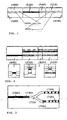
- Fig. 1 is a longitudinal cross-section of an SG-DBR laser.
- the reflectors are formed by two periodically modulated (sampled) gratings with different sampling periods.
- Fig. 2 is a schematic diagram of a GCSR laser structure.
- Fig. 3 is a top view (schematic) of the proposed "Y-SSG" laser.
- Fig. 4 is a schematic view of a ring resonator (S)SG laser.
- Fig. 5 is a transmission characteristic of a ring resonator.
- Fig. 6 is a principle scheme of the laser according to the inevntion, comprising an active element and a plurality of sections, being either transmission filters or reflectors.
- Fig. 7 is a principle scheme of prior-art lasers, comprising an active element and reflectors, said active element being bounded by said reflectors.
- Fig. 8 is a principle scheme of the second embodiment of the invention, comprising an active element and a plurality of sections, being parallel.
- Fig. 9 is a principle scheme of the fourth embodiment of the invention, comprising an active element and a serial concatenation of transmission filters ended by a reflector.
- the present invention discloses alternative laser structures, which ahe potentially the same tuning performance as (S)SG-DBR and GCSR lasers and which the output power does not pass through a long passive region.
- said devices there are passive or inactive regions on one side of the active region only.
- FIG. 7 A principle scheme of prior-art conventional Distributed Bragg Reflector (DBR) semiconductor laser is shown in Figure 7 .
- a schematic description of such a laser is shown in Figure 1 , showing a front (500) reflector, a rear reflector (510), an AR (anti-reflective coating), an active section (530) and a phase section (540).
- Tuning of said laser is limited by the fact that the relative tuning range (360) is restricted to the relative change in the refractive index of the tuning region. This means that the tuning range, under normal operating conditions, cannot exceed 10 nm. This is substantially less than the potential bandwidth, restricted by the width of the gain curve (350), which is about 100 nm.
- Such conventional DBR lasers can functionally be characterized as comprising a first part being a two-sided active section (300), for creating a light beam (310) by spontaneous emission over a bandwidth around some center frequency (370), as observed in said lasers characteristic (340). Said first part also guides said light beam.
- Such conventional DBR lasers further have two reflectors (330)(320). Said reflectors are bounding said two-sided active section (300), thus one at each side.
- a classical laser structure comprises (i) a two-sided active section/region, creating a light beam by spontaneous emission over a bandwidth around some center frequency and guiding said light beam, said active section performing optical amplification actions and (ii) two (inactive or passive) sections/regions, acting as reflectors. Said active section is bounded by said two reflectors.
- the invention can be characterized as comprising a two-sided active section/region (just as a classical laser) and a plurality of sections/regions.
- Said plurality of sections/regions defines a network of sections/regions.
- Said network of sections/regions is connected to one side of the active region.
- Said network comprises at least two resonator regions/sections.
- Said resonator regions/section can be either reflectors and regions/sections with a transmission characteristic.
- the principle scheme of the laser according to the invention comprising an active element (30) and a plurality of sections (50) (90) (100) (110), being resonators, thus being either transmission filters or reflectors, is shown in Figure 6 .
- the invention can be characterized as a device comprising (i) a substrate made of a semiconducting material, (ii) a two-sided active section on said substrate, said active section generating radiation by spontaneous emission over a bandwidth around some center frequency and guiding said radiation, said active section having amplification actions, and (iii) a plurality of sections on said substrate, all said sections being connected to one side of said active section, at least two of said sections including a waveguide system, defining either a transmission filter or a reflector.
- the device can further be comprising a plurality of power splitters, being exploited for interconnecting part of said inactive sections and connecting part of said sections with said active section. Said sections can be either active or inactive.
- connection of said network with said active section is an optical connection.
- Said connections of said sections are then also optical.
- Said device can then be denoted as a tunable integrated/semiconductor optical laser.
- Said amplification is then denoted to be an optical amplification.
- Said active section then also guides said light beam.
- Said reflectors and sections with transmission characteristics are commonly denoted as resonators.
- Said reflection and transmission sections are functionally characterized as having a reflection or transmission characteristic with a plurality of reflection or transmission peaks, commonly denoted as resonation peaks.
- Said reflection or transmission characteristic has spaced reflection or transmission maxima points providing a maximum reflection or transmission of an associated wavelength.
- the resonator characteristic thus has a plurality of spectral response peaks, preferably narrow spectral response peaks.
- Said resonator characteristic can be either regular, meaning that its resonation frequencies are all spaced apart by a same value, being the periodicity, or irregular, meaning that there is no fixed spacing between its resonation frequencies. Irregularity can be a random pattern of resonation frequencies or some structured pattern.
- Such a characteristic can be obtained via sampled gratings, which exhibit a comb-shaped reflection or transmission spectrum or via the so-called supergratings.
- Said gratings or supergratings can also be characterized as distributed reflectors or transmission sections.
- Sampled gratings can be described as structures in a waveguide system, having a periodically broken short-period structure including short period stripped regions alternating with non-stripped regions.
- the supergratings can be described as structures in a waveguide system having a diffractive grating having a plurality of repeating unit regions each having a constant length, thus forming a modulation period, and at least one parameter that determines the optical reflectivity or transmission of said diffractive grating varying depending on its position in each of said repeating unit regions along a direction of optical transmission in said laser, said diffractive grating extending by at least two modulation periods.
- Such a ring resonator has a comb-shaped transmission characteristic ( Figure 5 ).
- the operation of a ring resonator is similar to that of a classic Fabry-Perot resonator, which can easily be understood if one thinks of the cross-coupling of the two couplers in the ring as being the transmission mirrors in the FP-resonator.
- the invention can be further characterized by stating that the spacing of at least two transmission or reflective maxima points of the respective (inactive or even active) sections being essentially not equal or different, and at least one said transmission or reflective maxima of each of said (inactive or even active) sections being in correspondence with a wavelength of said created lightbeam. This correspondence is obtained by having at least one of said resonation peaks of at least two sections being overlapping or coinciding.
- the combination of said plurality of sections can be considered as a combined reflector, having a combination reflection action.
- Said optical amplification action of said active section and said combination reflection action of said combined reflector are causing lasing at least one of the reflection wavelengths of said combined reflector.
- FIG. 6 shows an example of a possible configuration although the invention is not limited hereto.
- the active section (30) is optically at one side connected with a plurality of sections (120), said plurality of sections comprising a transmission filter (50) and three reflectors (90)(100)(110).
- the lasing light (10) leaves the laser at the other side of the active section.
- (20) indicates the amplification action within said active section (10).
- Said connections (40), (60), (70) and (80) indicate the optical interconnectivity and should not be considered as physical connections.
- the transmission filters exploited in the invention have a transmission characteristic (150) with a plurality of transmission peaks. Alternatively it can be said that said transmission filters have spaced (spacing (130)) transmission maxima points providing a maximum transmission of an associated wavelength.
- the reflectors exploited in the invention have reflection characteristic (160) with a plurality of reflection peaks. Alternatively it can be said that said reflectors have spaced (spacing period (140)) reflective maxima points providing a maximum reflection of an associated wavelength.
- the spacing (130) (140) of said transmission or reflective maxima points of at least two of said sections are selected to be different. Said laser is therefore denoted an integrated semiconductor laser with different reflection or transmission sections.
- the transmission and reflection characteristic of said transmission filters and reflectors are positioned such that only one said transmission or reflective maxima of each of said sections being overlapping, meaning having a transmission or reflective maxima for the same frequency. Due to the different spacings of said transmission or reflective maxima points a small shift of one of said transmission or reflective maxima points results in an optical laser having a wide tunability. Said laser is therefore denoted widely wavelength tunable integrated semiconductor laser. Said shift can be due to current injections in said transmission or reflective sections. It can be said that said laser comprises of means for injecting current into part of said plurality of sections, resulting in said transmission or reflection characteristic being shifted in wavelength.
- the configuration of Figure 6 can for instance be achieved by using a power splitter (200) for connecting section (50) with sections (90)(100)(110).
- Said power splitter has a single port side (side connected to (50)) and a multi port side (side connected to (90)(100)(110), with three ports.
- FIG. 2 A schematic view of a prior art GCSR laser structure is shown in Figure 2 , showing an active section (600), a coupler section (610), a phase section (620), and a reflector (630), and the cross sections of said sections.
- Said coupler section and said reflector section have an essentially different resonance characteristic.
- Said coupler section does not have spaced resonation maxima points.
- a Y-structure as in Figure 3 is proposed with two reflectors (710), (720), placed on the same side of the active region (700). These two reflectors use sampled or super structure gratings to provide reflection combs with different periods; their design is the same as for (S)SG-DBR lasers.
- the power splitter (730) is used to split/combine the light leaving/entering the active region.
- Two phase control sections (740), (750) are shown in Figure 3 . One provides the correct phase relation between the signals reflected by the two reflectors, whereas the second provides control of the overall phase of the combined reflected signal.
- a separate phase control section could be placed in each of the arms of the Y.
- the branches of the Y-structure could be all-active, thus avoiding a (technologically more complex) transition from an active waveguide to a passive one.
- this has the disadvantage that the device will be more difficult to control, because power and wavelength control will be mixed. Therefore, passive waveguides for both branches of the Y-structure are preferred.
- a second structure which in a top view looks like in Figure 8 , is proposed.
- a plurality of reflectors (440) including reflectors (410, 420, 430) are placed on the same side of the active region. At least two of said reflectors use sampled or super structure gratings to provide reflections combs. At least two of said reflectors have reflection combs with different periods.
- the design of said reflectors is the same as for (S)SG-DBR lasers.
- the power splitter (450) is used to split and combine the light leaving/entering the active region.
- Phase control sections can be introduced. In one configuration one phase control section is placed between the active region and the reflectors and in all reflectors, except one, also a phase control section is provided. In another configuration only phase control sections are provided in said reflectors.
- a third structure as shown in Figure 4 , is proposed.
- the reflector consists of an active section (830), a ring resonator (800), which has a comb-shaped transmission characteristic ( Figure 5 ) and a (S)SG-reflector (810) with potentially even an anti-reflective coating (820).
- the operation of a ring resonator is similar to that of a classic Fabry-Perot resonator, which can easily be understood if one thinks of the cross-coupling of the two couplers in the ring as being the transmission mirrors in the FP-resonator.
- the tuning is again based on the "Vernier"-principle, as in conventional (S)SG-DBR lasers: the ring resonator and the (S)SG-reflector are designed to have slightly different peak-spacing in their transmission and reflection characteristics respectively, and lasing occurs at or near the wavelength where two peaks overlap each other.
- a phase section, used to align a longitudinal cavity mode with the two aligned peaks, could also be included in this structure. It could be placed either between the active section and the ring resonator, or between the ring and the (S)SG-reflector.
- a fourth structure as shown in Figure 9 , is proposed.
- This structure comprises an active region (900) bounded at one side by a serial concatenation of sections, being a plurality of transmission filters (940), including filters (910) (920), said concatenation ends with a reflector (930).
- At least two of said sections being either transmission filter or reflector, have a comb-shaped transmission characteristic.
- At least two of said sections, being either transmission filter or reflector are designed to have a slightly different peak-spacing in their characteristic.
- a phase section can be placed between any of said sections and between said active section and said sections.
- Said transmission filters can be either (S)SG-transmission filters or a ring-resonator.
- Said reflector is a (S)SG-reflector.
- a main feature of the proposed Y and ring-structures and any structure, exploiting a combination of the principles on which the proposed Y and ring structures are based, is that light is emitted directly from the active region without going through a passive region. This is expected to result in a higher efficiency and a lower degree of power variation during tuning.
- Typical reflectors can be designed to have a uniform envelope of the reflection peaks. These designs require long passive waveguides and the reflectivity at the reflection peaks is quite high. Both of these factors lead to a reduced efficiency in a two-sided reflector structure.
- the output power is not passing through a reflector, hence a high efficiency can be expected, and the high reflectivity is now an advantage. Therefore in the invention all said sections are optically connected to one side of said active region.
- the reflectors are preferably passive, the Y structure (of the first embodiment) and the structure of the second embodiment, does not suffer from the control problems present in the Y-laser, known from prior-art.
- the performance with respect to tuning and output power is expected to be similar to that of a GCSR laser, but the fabrication is easier.
- the number of process steps will be the same as for an SG/SSG, but lower than for a GCSR laser. Except for mask design the fabrication is nearly identical to that for SG/SSG DBR lasers, but AR coating of the facets may not be necessary when the grating is designed for high peak reflectivity. As an alternative one could use an absorbing region to kill off any unwanted reflection from the facet.
Claims (25)
- Appareil laser semi-conducteur intégré comprenant- un substrat constitué d'un matériau semi-conducteur,- une section active générant un rayonnement des deux côtés (30) sur ledit substrat,- une pluralité de sections non utilisée pour générer un rayonnement sur ledit substrat (120), ladite pluralité de sections étant optiquement connectée à une surface latérale de ladite section active des deux côtés, toutes lesdites sections étant connectées ensemble, chacune d'au moins deux desdites sections comprend un système de guide d'onde et comporte des points de maxima de résonance espacés fournissant une résonance maximale avec une longueur d'onde associée, moyennant quoi l'espacement d'au moins deux desdits points de maxima de résonance des sections respectives n'est pas égal, moyennant quoi lesdites au moins deux sections sont soit un filtre de transmission et un réflecteur couplés en série, soit deux réflecteurs couplés en parallèle, et- comprenant en outre un moyen pour injecter du courant dans au moins certaines desdites deux sections de sorte que lesdits points de maxima de résonance espacés sont décalés en longueur d'onde de sorte qu'au moins un desdits maxima de résonance de chacune des deux sections chevauche les autres, caractérisé en ce que lesdites au moins deux sections sont des résonateurs.
- Appareil selon la revendication 1, comprenant en outre au moins une section en phase.
- Appareil selon la revendication 2, dans lequel une section en phase est placée entre la section générant un rayonnement (30) et ladite pluralité de sections (120).
- Appareil selon la revendication 3, comprenant en outre une section en phase placée dans ladite pluralité de sections.
- Appareil selon l'une quelconque des revendications précédentes, comprenant en outre une pluralité de sections de phase, qui sont utilisées pour ajuster la phase de cavité ronde.
- Appareil selon l'une quelconque des revendications précédentes, dans lequel au moins une desdites sections comporte un revêtement anti-réfléchissant sur ses facettes.
- Appareil selon l'une quelconque des revendications précédentes, dans lequel au moins une desdites sections ne comporte pas de revêtement anti-réfléchissant sur ses facettes.
- Appareil selon l'une quelconque des revendications précédentes, dans lequel lesdits réflecteurs sont conçus afin d'avoir une enveloppe uniforme des pics de réflexion.
- Appareil selon l'une quelconque des revendications précédentes, dans lequel seulement un des maxima de résonance de chacune desdites sections est un résonateur chevauchant l'autre.
- Appareil selon l'une quelconque des revendications précédentes, dans lequel soit ledit filtre de transmission (50) présente des points de maxima de transmission espacés (130) fournissant une transmission maximale avec une longueur d'onde associée en tant que points de maxima de résonance, soit ledit réflecteur (90), (100), (110) présente des points de maxima réfléchissants espacés (140) fournissant une réflexion maximale avec une longueur d'onde associée en tant que points de maxima de résonance.
- Appareil selon l'une quelconque des revendications précédentes, dans lequel au moins l'une de ladite pluralité de sections est inactive.
- Appareil selon l'une quelconque des revendications précédentes, dans lequel au moins une de ladite pluralité de sections est active.
- Appareil selon l'une quelconque des revendications précédentes, dans lequel au moins un desdits systèmes de guide d'onde présente une structure ayant une période courte interrompue périodiquement comprenant des régions dépouillées de période courte alternant avec des régions non dépouillées.
- Appareil selon l'une quelconque des revendications précédentes, dans lequel au moins un desdits résonateurs comporte des maxima de résonance irréguliers.
- Appareil selon l'une quelconque des revendications 1 à 14 précédentes, dans lequel au moins un desdits systèmes de guide d'onde comporte une grille de diffraction ayant une pluralité de régions de motif de répétition ayant chacun une longueur constante, formant ainsi une période de modulation, et au moins un paramètre qui détermine la réflectivité optique ou la transmission de ladite grille de déviation variant en fonction de sa position dans chacune desdites régions de motif de répétition le long d'une direction de transmission optique dans ledit laser, ladite grille de diffraction s'étendant par au moins deux périodes de modulation.
- Appareil selon l'une quelconque des revendications précédentes, dans lequel au moins un desdits résonateurs présente des maxima de résonance réguliers.
- Appareil selon l'une quelconque des revendications 1 à 12 précédentes, dans lequel au moins un desdits systèmes de guide d'onde est un résonateur de cycle (800).
- Appareil selon l'une quelconque des revendications 11 à 16 précédentes, dans lequel ladite section active crée un faisceau lumineux par émission spontanée sur une bande passante autour d'une fréquence centrale et guide ledit faisceau lumineux et présente des actions d'amplification optique.
- Appareil selon la revendication 18, dans lequel la combinaison de ladite pluralité de sections présente une action de réflexion combinée et ladite action d'amplification optique de ladite section active entraînant une émission laser à au moins l'une des longueurs d'onde de réflexion de ladite combinaison.
- Appareil selon l'une quelconque des revendications précédentes, dans lequel la combinaison de ladite pluralité de sections présentant une action de réflexion combinée et ladite action d'amplification optique desdites sections actives est agencée afin d'entraîner une émission laser auxdits maxima de résonance.
- Appareil selon l'une quelconque des revendications 11 à 20 précédentes, comprenant en outre une pluralité de diviseurs de puissance (200), qui sont utilisés pour connecter certaines de ladite pluralité de sections et être connectés à ladite section active.
- Appareil selon les revendications 12 à 21, dans lequel ledit appareil est une concaténation en série de ladite section active (900) et une pluralité desdites sections (910), (920), (930).
- Appareil selon la revendication 21, dans lequel une connexion de ladite section active (400) est effectuée à un côté à port unique d'un diviseur de puissance (450) avec une connexion parallèle d'une pluralité de sections (410), (420), (430) à l'autre côté à port multiple dudit diviseur de puissance.
- Procédé destiné à fixer des fréquences d'émission laser d'un appareil laser semi-conducteur intégré, comprenant un substrat constitué d'un matériau semi-conducteur, une section active générant un rayonnement des deux côtés sur ledit substrat, une pluralité de sections non utilisées pour générer un rayonnement sur ledit substrat, ladite pluralité de sections étant connectée à une face latérale de ladite section active des deux côtés, toutes lesdites sections étant connectées ensemble, moyennant quoi au moins deux desdites sections ont des points de maxima de résonance espacés fournissant une résonance maximale avec une longueur d'onde associée, moyennant quoi l'espacement d'au moins deux desdits points de maxima de résonance des sections respectives est égal, moyennant quoi lesdites au moins deux sections sont soit un filtre de transmission et un réflecteur couplés en séries, soit deux réflecteurs couplés en parallèle, ledit procédé comprenant l'étape consistant à positionner lesdits points de maxima de résonance desdits résonateurs de sorte qu'une pluralité desdits maxima de résonance de chacune desdites sections soit des résonateurs qui se chevauchent les uns les autres, ladite pluralité définissant lesdites fréquences d'émission laser, caractérisé en ce que lesdites au moins deux desdites sections sont des résonateurs.
- Procédé destiné à modifier la fréquence d'émission laser d'un appareil laser semi-conducteur intégré selon la revendication 1, à partir d'une première fréquence vers une seconde fréquence, ladite seconde fréquence étant espacée de ladite première fréquence d'une première distance, ledit appareil laser semi-conducteur intégré comprenant un substrat constitué d'un matériau semi-conducteur, une section active générant un rayonnement des deux côtés sur ledit substrat, une pluralité de sections sur ledit substrat, ladite pluralité de sections étant connectée à un côté de ladite section active des deux côtés, toutes lesdites sections étant connectées ensemble, moyennant quoi au moins deux desdites sections ont des points de maxima de résonance espacés fournissant une résonance maximale avec une longueur d'onde associée, dans lequel l'espacement d'au moins deux desdits points de maxima de résonance des sections respectives n'est pas égal, moyennant quoi lesdites au moins deux sections sont soit un filtre de transmission et un réflecteur couplés en série, soit deux réflecteurs couplés en parallèle, ledit procédé comprenant l'étape consistant à modifier la position relative desdits points de maxima de résonance desdits résonateurs avec une seconde distance, qui est sensiblement plus petite que ladite première distance, caractérisé en ce que lesdites au moins deux desdites sections sont des résonateurs.
Priority Applications (1)
| Application Number | Priority Date | Filing Date | Title |
|---|---|---|---|
| EP20000870105 EP1058358B1 (fr) | 1999-05-17 | 2000-05-15 | Dispositif à laser semi-conducteur intégré accordable en longeur d'onde étendue |
Applications Claiming Priority (5)
| Application Number | Priority Date | Filing Date | Title |
|---|---|---|---|
| EP99870105 | 1999-05-17 | ||
| EP99870105 | 1999-05-17 | ||
| EP99870214A EP1094574A1 (fr) | 1999-10-18 | 1999-10-18 | Dispositif semiconducteur integré accordable en longeur d'onde étendu et méthode d'accorder en longeur d'onde étendu des dispositifs semiconducteur |
| EP99870214 | 1999-10-18 | ||
| EP20000870105 EP1058358B1 (fr) | 1999-05-17 | 2000-05-15 | Dispositif à laser semi-conducteur intégré accordable en longeur d'onde étendue |
Publications (2)
| Publication Number | Publication Date |
|---|---|
| EP1058358A1 EP1058358A1 (fr) | 2000-12-06 |
| EP1058358B1 true EP1058358B1 (fr) | 2008-10-29 |
Family
ID=27223754
Family Applications (1)
| Application Number | Title | Priority Date | Filing Date |
|---|---|---|---|
| EP20000870105 Expired - Lifetime EP1058358B1 (fr) | 1999-05-17 | 2000-05-15 | Dispositif à laser semi-conducteur intégré accordable en longeur d'onde étendue |
Country Status (1)
| Country | Link |
|---|---|
| EP (1) | EP1058358B1 (fr) |
Cited By (1)
| Publication number | Priority date | Publication date | Assignee | Title |
|---|---|---|---|---|
| WO2020128098A1 (fr) | 2018-12-21 | 2020-06-25 | Fraunhofer-Gesellschaft zur Förderung der angewandten Forschung e.V. | Système et procédé de génération et de vérification de rayonnement térahertz |
Families Citing this family (6)
| Publication number | Priority date | Publication date | Assignee | Title |
|---|---|---|---|---|
| DE10105731A1 (de) * | 2001-02-08 | 2002-09-05 | Infineon Technologies Ag | Laserstruktur und Verfahren zur Einstellung einer definierten Wellenlänge |
| US6891865B1 (en) | 2002-02-15 | 2005-05-10 | Afonics Fibreoptics, Ltd. | Wavelength tunable laser |
| US8218151B2 (en) | 2009-03-12 | 2012-07-10 | Tel Aviv University Future Technology Development Ltd | Light-emitting intra-cavity interferometric sensors |
| EP2993743B1 (fr) | 2014-09-02 | 2017-05-10 | Huawei Technologies Co., Ltd. | Laser accordable et procédé de réglage d'un mode d'émission laser |
| EP3029783B1 (fr) | 2014-12-01 | 2020-03-04 | Huawei Technologies Co., Ltd. | Laser accordable à canaux multiples |
| EP3051638A1 (fr) | 2015-01-27 | 2016-08-03 | Huawei Technologies Co., Ltd. | Laser accordable et procédé de réglage d'un laser |
Family Cites Families (5)
| Publication number | Priority date | Publication date | Assignee | Title |
|---|---|---|---|---|
| JPS63229796A (ja) * | 1987-03-18 | 1988-09-26 | Fujitsu Ltd | 光半導体素子 |
| US5325392A (en) * | 1992-03-06 | 1994-06-28 | Nippon Telegraph And Telephone Corporation | Distributed reflector and wavelength-tunable semiconductor laser |
| US5537432A (en) * | 1993-01-07 | 1996-07-16 | Sdl, Inc. | Wavelength-stabilized, high power semiconductor laser |
| US5398256A (en) * | 1993-05-10 | 1995-03-14 | The United States Of America As Represented By The United States Department Of Energy | Interferometric ring lasers and optical devices |
| US6104739A (en) * | 1997-12-24 | 2000-08-15 | Nortel Networks Corporation | Series of strongly complex coupled DFB lasers |
-
2000
- 2000-05-15 EP EP20000870105 patent/EP1058358B1/fr not_active Expired - Lifetime
Cited By (1)
| Publication number | Priority date | Publication date | Assignee | Title |
|---|---|---|---|---|
| WO2020128098A1 (fr) | 2018-12-21 | 2020-06-25 | Fraunhofer-Gesellschaft zur Förderung der angewandten Forschung e.V. | Système et procédé de génération et de vérification de rayonnement térahertz |
Also Published As
| Publication number | Publication date |
|---|---|
| EP1058358A1 (fr) | 2000-12-06 |
Similar Documents
| Publication | Publication Date | Title |
|---|---|---|
| US6728279B1 (en) | Widely wavelength tunable integrated semiconductor device and method for widely tuning semiconductor devices | |
| US7145923B2 (en) | Tuneable laser | |
| EP1281221B1 (fr) | Modeles de miroir et de cavite ameliores destines a des lasers pour reflecteur de bragg repartis a reseau de diffraction echantillonne | |
| US5333219A (en) | Asymmetric Y-branch optical device | |
| US7653093B2 (en) | Widely tunable twin guide laser structure | |
| US7643532B2 (en) | Manufacturable sampled grating mirrors | |
| US7382817B2 (en) | V-coupled-cavity semiconductor laser | |
| EP1094574A1 (fr) | Dispositif semiconducteur integré accordable en longeur d'onde étendu et méthode d'accorder en longeur d'onde étendu des dispositifs semiconducteur | |
| EP2064785B9 (fr) | Dispositif laser à cavité couplé et accordé par vernier avec une moulure comprenant des évidements pour suppression du mode longitudinal | |
| JP2002299755A (ja) | 迅速かつ広帯域にわたって同調可能なレーザ | |
| US7106778B2 (en) | Tuneable laser | |
| EP1413021B1 (fr) | Laser accordable | |
| EP1058358B1 (fr) | Dispositif à laser semi-conducteur intégré accordable en longeur d'onde étendue | |
| Ishii et al. | A tunable distributed amplification DFB laser diode (TDA-DFB-LD) | |
| JP4690521B2 (ja) | 広い範囲の波長で同調可能な集積化された半導体装置及び広い範囲の波長で同調可能な半導体装置のための方法 | |
| US7106765B2 (en) | Tuneable laser | |
| Rigole et al. | Access to 20 evenly distributed wavelengths over 100 nm using only a single current tuning in a four-electrode monolithic semiconductor laser | |
| JP2000223774A (ja) | 波長可変光源 | |
| US20040081211A1 (en) | Tunable laser | |
| Sarlet et al. | Tunable laser diodes | |
| Rana et al. | Microring resonator based widely tunable semiconductor lasers | |
| GB2378315A (en) | tuneable Laser |
Legal Events
| Date | Code | Title | Description |
|---|---|---|---|
| PUAI | Public reference made under article 153(3) epc to a published international application that has entered the european phase |
Free format text: ORIGINAL CODE: 0009012 |
|
| AK | Designated contracting states |
Kind code of ref document: A1 Designated state(s): AT BE CH CY DE DK ES FI FR GB GR IE IT LI LU MC NL PT SE |
|
| AX | Request for extension of the european patent |
Free format text: AL;LT;LV;MK;RO;SI |
|
| 17P | Request for examination filed |
Effective date: 20010207 |
|
| AKX | Designation fees paid |
Free format text: AT BE CH CY DE DK ES FI FR GB GR IE IT LI LU MC NL PT SE |
|
| 17Q | First examination report despatched |
Effective date: 20060317 |
|
| GRAP | Despatch of communication of intention to grant a patent |
Free format text: ORIGINAL CODE: EPIDOSNIGR1 |
|
| RTI1 | Title (correction) |
Free format text: TUNABLE INTEGRATED SEMICONDUCTOR LASER APPARATUS |
|
| RIN1 | Information on inventor provided before grant (corrected) |
Inventor name: BUUS, JENS Inventor name: BAETS, ROEL Inventor name: SARLET, GERT |
|
| GRAS | Grant fee paid |
Free format text: ORIGINAL CODE: EPIDOSNIGR3 |
|
| GRAA | (expected) grant |
Free format text: ORIGINAL CODE: 0009210 |
|
| AK | Designated contracting states |
Kind code of ref document: B1 Designated state(s): AT BE CH CY DE DK ES FI FR GB GR IE IT LI LU MC NL PT SE |
|
| REG | Reference to a national code |
Ref country code: GB Ref legal event code: FG4D |
|
| REG | Reference to a national code |
Ref country code: CH Ref legal event code: EP |
|
| REG | Reference to a national code |
Ref country code: IE Ref legal event code: FG4D |
|
| REF | Corresponds to: |
Ref document number: 60040634 Country of ref document: DE Date of ref document: 20081211 Kind code of ref document: P |
|
| REG | Reference to a national code |
Ref country code: SE Ref legal event code: TRGR |
|
| NLV1 | Nl: lapsed or annulled due to failure to fulfill the requirements of art. 29p and 29m of the patents act | ||
| PG25 | Lapsed in a contracting state [announced via postgrant information from national office to epo] |
Ref country code: AT Free format text: LAPSE BECAUSE OF FAILURE TO SUBMIT A TRANSLATION OF THE DESCRIPTION OR TO PAY THE FEE WITHIN THE PRESCRIBED TIME-LIMIT Effective date: 20081029 Ref country code: ES Free format text: LAPSE BECAUSE OF FAILURE TO SUBMIT A TRANSLATION OF THE DESCRIPTION OR TO PAY THE FEE WITHIN THE PRESCRIBED TIME-LIMIT Effective date: 20090209 |
|
| PG25 | Lapsed in a contracting state [announced via postgrant information from national office to epo] |
Ref country code: NL Free format text: LAPSE BECAUSE OF FAILURE TO SUBMIT A TRANSLATION OF THE DESCRIPTION OR TO PAY THE FEE WITHIN THE PRESCRIBED TIME-LIMIT Effective date: 20081029 Ref country code: PT Free format text: LAPSE BECAUSE OF FAILURE TO SUBMIT A TRANSLATION OF THE DESCRIPTION OR TO PAY THE FEE WITHIN THE PRESCRIBED TIME-LIMIT Effective date: 20090330 Ref country code: FI Free format text: LAPSE BECAUSE OF FAILURE TO SUBMIT A TRANSLATION OF THE DESCRIPTION OR TO PAY THE FEE WITHIN THE PRESCRIBED TIME-LIMIT Effective date: 20081029 |
|
| PG25 | Lapsed in a contracting state [announced via postgrant information from national office to epo] |
Ref country code: DK Free format text: LAPSE BECAUSE OF FAILURE TO SUBMIT A TRANSLATION OF THE DESCRIPTION OR TO PAY THE FEE WITHIN THE PRESCRIBED TIME-LIMIT Effective date: 20081029 |
|
| RAP2 | Party data changed (patent owner data changed or rights of a patent transferred) |
Owner name: UNIVERSITEIT GENT Owner name: IMEC |
|
| PLBE | No opposition filed within time limit |
Free format text: ORIGINAL CODE: 0009261 |
|
| STAA | Information on the status of an ep patent application or granted ep patent |
Free format text: STATUS: NO OPPOSITION FILED WITHIN TIME LIMIT |
|
| 26N | No opposition filed |
Effective date: 20090730 |
|
| PG25 | Lapsed in a contracting state [announced via postgrant information from national office to epo] |
Ref country code: MC Free format text: LAPSE BECAUSE OF NON-PAYMENT OF DUE FEES Effective date: 20090531 |
|
| REG | Reference to a national code |
Ref country code: CH Ref legal event code: PL |
|
| PG25 | Lapsed in a contracting state [announced via postgrant information from national office to epo] |
Ref country code: LI Free format text: LAPSE BECAUSE OF NON-PAYMENT OF DUE FEES Effective date: 20090531 Ref country code: CH Free format text: LAPSE BECAUSE OF NON-PAYMENT OF DUE FEES Effective date: 20090531 |
|
| REG | Reference to a national code |
Ref country code: IE Ref legal event code: MM4A |
|
| PG25 | Lapsed in a contracting state [announced via postgrant information from national office to epo] |
Ref country code: IE Free format text: LAPSE BECAUSE OF NON-PAYMENT OF DUE FEES Effective date: 20090515 |
|
| PG25 | Lapsed in a contracting state [announced via postgrant information from national office to epo] |
Ref country code: GR Free format text: LAPSE BECAUSE OF FAILURE TO SUBMIT A TRANSLATION OF THE DESCRIPTION OR TO PAY THE FEE WITHIN THE PRESCRIBED TIME-LIMIT Effective date: 20090130 |
|
| PG25 | Lapsed in a contracting state [announced via postgrant information from national office to epo] |
Ref country code: LU Free format text: LAPSE BECAUSE OF NON-PAYMENT OF DUE FEES Effective date: 20090515 |
|
| PG25 | Lapsed in a contracting state [announced via postgrant information from national office to epo] |
Ref country code: CY Free format text: LAPSE BECAUSE OF FAILURE TO SUBMIT A TRANSLATION OF THE DESCRIPTION OR TO PAY THE FEE WITHIN THE PRESCRIBED TIME-LIMIT Effective date: 20081029 |
|
| REG | Reference to a national code |
Ref country code: FR Ref legal event code: PLFP Year of fee payment: 17 |
|
| REG | Reference to a national code |
Ref country code: FR Ref legal event code: PLFP Year of fee payment: 18 |
|
| REG | Reference to a national code |
Ref country code: FR Ref legal event code: PLFP Year of fee payment: 19 |
|
| PGFP | Annual fee paid to national office [announced via postgrant information from national office to epo] |
Ref country code: DE Payment date: 20190418 Year of fee payment: 20 Ref country code: IT Payment date: 20190418 Year of fee payment: 20 |
|
| PGFP | Annual fee paid to national office [announced via postgrant information from national office to epo] |
Ref country code: BE Payment date: 20190424 Year of fee payment: 20 Ref country code: FR Payment date: 20190418 Year of fee payment: 20 Ref country code: SE Payment date: 20190425 Year of fee payment: 20 |
|
| PGFP | Annual fee paid to national office [announced via postgrant information from national office to epo] |
Ref country code: GB Payment date: 20190423 Year of fee payment: 20 |
|
| REG | Reference to a national code |
Ref country code: DE Ref legal event code: R071 Ref document number: 60040634 Country of ref document: DE |
|
| REG | Reference to a national code |
Ref country code: GB Ref legal event code: PE20 Expiry date: 20200514 |
|
| REG | Reference to a national code |
Ref country code: SE Ref legal event code: EUG |
|
| REG | Reference to a national code |
Ref country code: BE Ref legal event code: MK Effective date: 20200515 |
|
| PG25 | Lapsed in a contracting state [announced via postgrant information from national office to epo] |
Ref country code: GB Free format text: LAPSE BECAUSE OF EXPIRATION OF PROTECTION Effective date: 20200514 |