EP1413021B1 - Laser accordable - Google Patents
Laser accordable Download PDFInfo
- Publication number
- EP1413021B1 EP1413021B1 EP02747608A EP02747608A EP1413021B1 EP 1413021 B1 EP1413021 B1 EP 1413021B1 EP 02747608 A EP02747608 A EP 02747608A EP 02747608 A EP02747608 A EP 02747608A EP 1413021 B1 EP1413021 B1 EP 1413021B1
- Authority
- EP
- European Patent Office
- Prior art keywords
- grating
- laser
- wavelength
- chirp
- mirror
- Prior art date
- Legal status (The legal status is an assumption and is not a legal conclusion. Google has not performed a legal analysis and makes no representation as to the accuracy of the status listed.)
- Expired - Fee Related
Links
Images


Classifications
-
- H—ELECTRICITY
- H01—ELECTRIC ELEMENTS
- H01S—DEVICES USING THE PROCESS OF LIGHT AMPLIFICATION BY STIMULATED EMISSION OF RADIATION [LASER] TO AMPLIFY OR GENERATE LIGHT; DEVICES USING STIMULATED EMISSION OF ELECTROMAGNETIC RADIATION IN WAVE RANGES OTHER THAN OPTICAL
- H01S5/00—Semiconductor lasers
- H01S5/06—Arrangements for controlling the laser output parameters, e.g. by operating on the active medium
- H01S5/062—Arrangements for controlling the laser output parameters, e.g. by operating on the active medium by varying the potential of the electrodes
- H01S5/0625—Arrangements for controlling the laser output parameters, e.g. by operating on the active medium by varying the potential of the electrodes in multi-section lasers
- H01S5/06255—Controlling the frequency of the radiation
- H01S5/06256—Controlling the frequency of the radiation with DBR-structure
-
- H—ELECTRICITY
- H01—ELECTRIC ELEMENTS
- H01S—DEVICES USING THE PROCESS OF LIGHT AMPLIFICATION BY STIMULATED EMISSION OF RADIATION [LASER] TO AMPLIFY OR GENERATE LIGHT; DEVICES USING STIMULATED EMISSION OF ELECTROMAGNETIC RADIATION IN WAVE RANGES OTHER THAN OPTICAL
- H01S5/00—Semiconductor lasers
- H01S5/10—Construction or shape of the optical resonator, e.g. extended or external cavity, coupled cavities, bent-guide, varying width, thickness or composition of the active region
- H01S5/12—Construction or shape of the optical resonator, e.g. extended or external cavity, coupled cavities, bent-guide, varying width, thickness or composition of the active region the resonator having a periodic structure, e.g. in distributed feedback [DFB] lasers
- H01S5/1206—Construction or shape of the optical resonator, e.g. extended or external cavity, coupled cavities, bent-guide, varying width, thickness or composition of the active region the resonator having a periodic structure, e.g. in distributed feedback [DFB] lasers having a non constant or multiplicity of periods
- H01S5/1212—Chirped grating
Definitions
- This invention relates to tuneable lasers and has particular, but not necessarily exclusive, reference to tuneable lasers for use in telecommunications systems operating in the C-band, namely within the band of 1530 to 1570 nm.
- the term "light” will be used in the sense that it is used in optical systems to meari not just visible light but also electromagnetic radiation having a wavelength between 1000 nanometres (nm) and 3000 nm.
- Narrowband lasers are important for a number of applications in optical telecommunications and signal processing applications. These include multiple channel optical telecommunications networks using wavelength division multiplexing (WDM). Such networks can provide advanced features, such as wavelength routing, wavelength conversion, adding and dropping of channels and wavelength manipulation in much the same way as in time slot manipulation in time division multiplexed systems. Many of these systems operate in the C-band in the range 1530 to 1570 nm.
- WDM wavelength division multiplexing
- Tuneable lasers for use in such optical communications systems, particularly in connection with the WDM telecommunication systems, are known.
- a known uneable system comprises a plurality of individually wavelength distributed Bragg reflectors (DBR) lasers, which can be individually selected, or by a wide tuning range tuneable laser that can be electronically driven to provide the wavelength required.
- DBR distributed Bragg reflectors
- Limited tuning range tuneable lasers that rely upon thermal effects for tuning are also known.
- the document EP 0 559 192 A discloses a distributed reflector and wavelength tunable semiconductor laser.
- US 4896325 discloses a wavelength tuneable laser having sampled gratings at the front and rear of its gain region.
- the gratings produce slightly different reflection combs which provide feedback into the device.
- the gratings can be current tuned in wavelength with respect to each other.
- Coincidence of a maximum from each of the front and rear gratings is referred to as a supermode.
- To switch the device between supermodes requires a small incremental electrical current into one of the gratings to cause a different pair of maxima to coincide in the manner of a vernier.
- electrical currents to the two gratings so that the corresponding maxima track, continuous tuning within a supermode can be achieved.
- the reflection spectrum of the known sampled grating structures have a Sinc squared envelope which limits the total optical bandwidth over which the laser can reliably operate as a single mode device.
- the front and rear gratings operate in a vernier mode, in which the wavelengths of correspondence determine a supermode wavelength.
- the sampled grating DBR does not have a constant ptical cavity length as it goes from one supermode to another, which can result in mode hopping if great care is not taken to avoid it.
- the present invention is defined in claim 1.
- a monolithic tuneable laser comprising an active section bounded at one end by a first mirror and at the other end by a second mirror, characterised in that each of the mirrors is in the form of a chirp grating, and in that at least one of the mirrors has a plurality of selectable electrodes to enable the grating to be selectively activated to produce a selective reflection at a predetermined wavelength.
- the gratings may be located in a material having a refractive index variable in response by the passage of a current therethrough and the grating may be activated at the specific wavelength by the variation in a local region of the refractive index.
- the wavelength position of the specific reflection may be altered by varying the refractive index of at least that region of the grating and also the portion of the grating between the region and the gain section.
- One of the gratings is a front grating and the other a rear grating, with the selectable electrodes being located on either the rear or the front grating, or both.
- the pitch characteristics of the front and rear chirp gratings being the grating pitch against distance along the grating, may be substantially identical and the chirp gratings may be linear.
- the two chirp profiles have different chirp characteristics so that the optical cavity length is constant or substantially constant at different wavelengths.
- the reflectivity of the rear mirror may be greater then the reflectivity of the front mirror.
- the front and rear mirrors may be formed by electron beam writing of the grating patterns and the mark space ratio of the rear mirror may be substantially unity and the mark space ratio of the front mirror may be substantially different to unity.
- the reflectivity of the rear mirror is typically 50% and the reflectivity of the front mirror is typically 30%.
- the pitch spacings of the rear mirror chirp may be at its lowest adjacent the gain section and the pitch spacings of the front mirror may be at its highest adjacent the gain section.
- phase change section between the gain section and the rear grating.
- One or more of the tuning electrodes within the optical cavity may be utilised as a phase control means to reduce or eliminate mode hopping.
- Light power may be coupled out from both ends of the laser, and both gratings may be substantially identical.
- composition of the mirror sections typically is formed of Group III-V semiconductor layers of different refractive index.
- the present invention also provides a method of operating a laser in which the rear grating has a plurality of selectable electrodes and in which the selection of a wavelength occurs by passing current through one of the electrodes to reduce the refractive index of the portion of the chirp grating affected by the electrode in which those electrodes capable of reducing the refractive index of the portion of the chirp effective at a shorter wavelength are also actuated to prevent the formation of a distorted reflection peak.
- the wavelengths of interest referred to above are the wavelengths of light in free space.
- n eff refractive index
- the actual wavelength of the light within that medium which will be referred to herein as ⁇ ' is the wavelength ⁇ divided by the value for the refractive index n eff .
- ⁇ ' ⁇ / n eff where n eff is the effective refractive index of the medium as seen by the propagating light.
- the glass (silica) fibres which are commonly used in telecommunications systems, have low loss regions at about 1100 nm 1300 nm and 1500 nm. These regions are about 100 nm wide and consequently much work is done on producing lasers that produce light in the low loss regions. The same is true for the tuneable laser of the present invention.
- the specific examples of the invention are designed to work in the C- Band, but the invention could be used for other wavelengths if required and if new types of fibre optical cables become available.
- a chirp grating is a form of Bragg grating which has a substantially continuous variation in the wavelength at which it reflects light along its length. It is thus distinguished from a normal DBR, which reflects at a single wavelength, and also from a sampled grating DBR which reflects at a plurality of discrete wavelengths.
- a chirp grating is formed at the interface between two materials of different refractive index and can be represented graphically as a sinusoidal shaped waveform, or as a castellated form.
- the physical shape of the grating is dependant upon the etching technique employed and may result in a castellated form, particularly when a dry etching process is used to produce the grating, e.g. reactive ion etching.
- the grating is formed as an interface 1 between the upper layer of material 2 of a low refractive index and a lower layer 3 of a higher refractive index.
- the pitch ⁇ of the grating is gradually increased along the length of the grating from ⁇ s at the short pitch end of the chirp grating to ⁇ L at the long pitch end of the grating.
- the increase in pitch is deliberately exaggerated to demonstrate what is happening. In practise, for typical telecommunications bands, the increase in pitch length over the whole of the grating will be small, namely about 2.5%.
- the grating reflects light of a wavelength corresponding to 1530 nm and at the long end the grating reflects light at a wavelength corresponding to 1570 nm.
- the reflection wavelength there is a 40 nm variation in the reflection wavelength over the length of the grating, which is about 2.5% of the average wavelength of 1550 nm.
- the refractive index n of the material used in the production of the chirp grating through which the majority of the light passes is quarternary material (InGaAsP) and the refractive index n of the material varies, as stated above, with the wavelength of light passing through the material.
- n at 1570 nm is 3.33
- at 1550 nm n is 3.38
- at 1530 nm n is 3.43.
- n decreases by about 3% from 1530 nm to 1570 nm.
- Fig 1b there is a graph showing how the pitch of the grating varies along its length, with the pitch, ⁇ , in the vertical axis and the length of the grating x on the horizontal axis.
- the pitch values, ⁇ , along the length of the grating can be plotted directly against the length and a line 4 is generated.
- the line 4 can be straight or can be curved depending on how the pitch is varied along the length of the grating. If the increase in grating pitch is at a constant rate, the line is straight and the grating is called a linear chirp grating. If the increase in grating pitch along the grating is uniform, in other words in the direction of increasing ⁇ , each ⁇ is a certain small constant amount greater in length than the one before it, then in this case line 4 will not be linear but will curve downwards as the line increasingly goes to the right as shown in the drawing at 4a.
- this demonstrates the effect of light passing along a chirp grating.
- the grating is shown as a sinusoidal interface 5 between an upper layer 6 of a lower refractive index and a lower layer 7 of higher refractive index.
- the waveguide of the assembly of high refractive index is shown at 8, separated from the lower layer 7 of the chirp grating by an intermediate layer 10 of low refractive index.
- the waveguide 8 is a low refractive index substrate 11.
- the two layers 10 and 11 serve to contain the light passing through the waveguide 8.
- superimposed on the layer structure is a graphical representation of the wave front of the light passing through from left to right as at 12 in the direction of the arrows 12a.
- Trace 13 is an indication of the intensity of the light in the layers of the assembly with the higher intensity levels to the right of the figure. It can be seen that most of the light passes through the waveguide 8 of high refractive index.
- Fig 3 are box diagrams of intensity of light, I, in the vertical axis and wavelength, ⁇ ', in the horizontal axis.
- a box of light consisting of a plurality of wavelengths is admitted into the grating as shown at 14 on the left hand side of the drawing, the envelope is complete and represents all of the wavelengths between ⁇ ' 1 and ⁇ ' 2 , which are widely, separated wavelengths.
- the chirp grating reflects certain of the wavelengths, for example between ⁇ ' s and ⁇ ' L
- the emerging box of wavelengths 15 has a gap 16 which corresponds to those wavelengths between ⁇ ' s and ⁇ ' L reflected by the chirp grating.
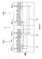
- two chirp gratings shown generally by 17 and 18 can be created on either side of a gain section 19. Initially, for the ease of understanding of the invention, the gain section will be ignored.
- the two chirp gratings 17 and 18 are shown superimposed on the pitch vs distance plots 20 and 21, which form the lower portion of Fig 5.
- These pitch vs distance plots show pitch ⁇ in the vertical axis and distance x along the grating in the horizontal axis.
- the grating 17 will be termed the front grating and the grating 18 will be termed the rear grating.
- the shape of the graph of pitch spacing from ⁇ S to ⁇ L vs. distance as represented by trace 22 for grating 17 is the same as that for grating 18 as shown by trace 23.
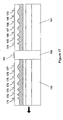
- the interface between the materials of different refractive index which goes to make up the chirp grating can be produced in the form of castellations, and are illustrated in Fig 6a at 24 and 25.
- the preferred method of producing the castellations is to produce layer 7 and to etch grooves into the layer and then to grow layer 6 on top of the layer 7 containing the grooves.
- the width of the grooves is then conventionally referred to as a space, S, and the distance between the grooves is referred to as a mark, M.
- the width of the mark M and the spacing S can be varied, so as to alter the mark/space ratio (M/S ratio).
- the rear grating has a mark/space ratio of 1 whereas the front grating has a mark/space ratio greater or less than 1.
- Fig 6b is a graph of reflection ⁇ against distance x, and it can be seen that the front chirp has a reflection coefficient of about 30% and the rear grating has a reflection coefficient of about 50%. This is shown by the traces 26 for the front grating and 27 for the rear grating.
- the front and rear chirp gratings can be either of the same chirp profile, or have different profiles, for reasons that are set out in a later part of the specification. If the chirp gratings have the same profile then a phase section functionality is required. In the circumstance where the front and rear chirps have the same chirp profile then this means that the slopes 22 and 23 are identical, as shown in Fig 5.
- the distance 28 between two corresponding positions 33, 34 at the short ends of the gratings, as shown in Fig 4, will be the same as the distance 29 between two corresponding positions 35, 36 at the long ends of the gratings. The significance of this will be seen below.
- the effect of placing a gain medium in the region 19 is that light can be generated in that region and this generated light will initially pass outwards in both directions from the centre.
- Light which is of a longer wavelength than that which can be reflected by the grating at any point does not in effect "see” the grating and is unaffected by it.
- light of a wavelength longer than ⁇ ' L will be substantially unaffected by the grating but be partially absorbed by the waveguide, and light of shorter wavelengths will be variously affected.
- light having wavelengths between ⁇ ' L and ⁇ ' S passing to the left of the gain section in the direction of the front grating will be reflected back as at 30 to 31.
- the light passing to the right into the rear grating will also be reflected back but as the shorter wavelengths are reflected first, and do not have to pass through the longer wavelength sections of the grating, they are not attenuated to the same extent as light of the same wavelengths passing through the front grating. Again the light of longer wavelengths, which is reflected by the rear gratings of pitch ⁇ L , does not "see" the shorter pitch gratings. Thus, the light at all wavelengths is reflected more uniformly by the rear grating than by the front grating.
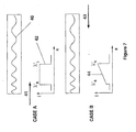
- FIG 7 illustrates what happens with a higher strength reflecting grating.
- Case A the reflection of a box of wavelengths passing along a chirp grating 40, from shorter to longer pitch in the direction 41, is illustrated at 42 in the box diagram of light intensity I vs. distance x.
- the reflection is substantially the same at the shorter wavelengths ⁇ ' S as at the longer wavelengths ⁇ ' L .
- Case B the short wavelengths ⁇ ' S are reflected to a far lesser extent than the longer wavelengths ⁇ ' L This is as shown in the lower box diagram at 44. It can be seen that the shorter wavelengths are strongly attenuated compared to the longer wavelengths.
- the rear strong mirror has ⁇ S adjacent the gain section and the front mirror has ⁇ L adjacent the gain section.
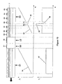
- FIG. 9 illustrates in cross section the upper portion a laser assembly in accordance with one embodiment of the invention.
- the laser comprises a four-part assembly of a central gain section 50 with a front mirror in the form of a chirp grating 51 and a rear mirror in the form of a chirp grating 52.
- a phase change section 53 the function of which will be described below.
- Fig 10 is a plot of grating pitch A against distance x, for an embodiment where the front and rear gratings have identical chirp profiles. This is shown by the traces 54, 55. It will be seen that trace 55 has a region 56, shown dotted below the main portion of the trace, for reasons which will be explained below.
- the electrode 57 can be used to inject current into the gain section to make it create light.
- the electrode 58 can be used to control the phase section as described below and the electrodes 59 to 65 are able to inject current into different regions of the rear grating 52.
- the chirp sections are capable of reflecting light in the range of 1530 to 1570 nm the wavelengths of light within that range will be internally reflected. Light outside of the reflecting wavelengths will be absorbed or will be emitted from the ends of the laser. The laser will not lase because the intensity of the light at all of the frequencies in the range 1530 to 1570 nm is below the lasing threshold.
- the selection of the particular wavelength is effected by passing a current through an electrode such as electrode 62 above the portion of the chirp grating which corresponds to the region 56 in the trace 55.
- the effect of the passage of current is to increase the current density in that region of the grating, which lowers the refractive index of the grating layer 7 just below the electrode 62.
- the lowering of the refractive index has the effect of making the grating reflect at a lower wavelength, which is the same effect as would be obtained by shortening the grating pitches in that region.
- the laser could only be tuned to as many different wavelengths as there are electrodes 59 to 65.
- the device can be made continuously tuneable if the materials from which the chirp gratings are constructed have a sufficiently variable refractive index.
- Fig 12 illustrates how this can be put into effect.
- Fig 12 there is shown the rear mirror chirp grating under three different conditions.
- a current is passed through electrode 106.
- the current is half that required to cause the maximum reduction in the refractive index, n, of the material of the chirp grating below the electrode 106, which is equivalent to material 7 in Fig 10.
- the result of this is to displace downwards the portion 111 of the line 110. This results in a selection of a particular wavelength at which the laser can lase in exactly the same manner as described above with reference to Fig 10.
- the electrodes 100 to 105 When the current passing through the electrode 106 is the maximum which can be applied to reduce n, and thus the maximum amount of fine tuning has occurred, the electrodes 100 to 105 will be passing a current which corresponds to half of the total reduction of n in the material in layer 7 below electrodes 100 to 105.
- the current is removed from electrode 106 and is applied to the next adjacent electrode (or any other selected electrode) and the sequence of actions is repeated.
- the laser can be tuned over the entire 1530nm to 1570nm waveband.
- Fig 13 The selectivity of the chirp at a particular wavelength can be enhanced as shown schematically in Fig 13. This Figure is closely similar to Fig 12 but shows what happens when two adjacent sections of the chirp grating are moved together.
- Fig 13 In the upper portion of Fig 13 the rear chirp grating is shown in the same position as in Fig 12. This is also the case for the central portion of Fig 13, where current applied to electrode 106 has caused a lowering of the line 111 to the position half way down to its maximum extent. If the current is passed through electrode 105 this causes the line 113 to be lowered and the current passing through electrode 106 is increased at the same rate so that lines 111a and 113 move down in synchronism. This means that the grating selectivity is increased by the enhanced reflectivity.
- each of the 104, 103 and 102 electrodes have just sufficient current injection to avoid degradation of the reflection peak.
- the current in lower wavelength adjacent electrodes will be in excess of half that of the higher wavelength adjacent electrode.
- these profiled currents are referred to as half currents..
- each electrode that can be installed over the chirp, the greater the number of regions that can be brought into coincidence and the smaller each reduction in refractive index needed at any point to tune the laser. For example, for a range of 40 nm total tuning, if twelve different electrode positions are used, then each is only required to tune through a range of 4 nm, whilst ensuring the desired band coverage is obtained.
- the laser can be tuned over the whole of the desired wavelength range, depending on the bandwidth of the original gratings.
- a constant optical cavity length is a length in which a constant number of unit standing wave periods can be supported.
- N is the number of standing wave periods, which can be supported
- L is the physical cavity length
- n is the cavity refractive index
- phase change section 53 controllable by electrode 58 is to give a constant optical cavity length for the embodiment of the invention shown in Fig 9.
- the phase change section can also be used to compensate for ageing of the laser. It can also be used to correct small changes occurring as a result of thermal effects.
- a number of ways of substantially eliminating or ameliorating the optical cavity length change have been developed.
- a number of alternative methods of operating the laser to effect optimum performance have also been developed.
- a way to substantially eliminate the change in the optical cavity length, as the laser is tuned to different wavelengths, is to design and construct the chirp gratings so that as they are written, the chirp characteristics of the front and rear chirps are slightly different, so that the number of standing waves as set out in the above equation (2) is the same irrespective of the wavelength selected.
- Tuning is thus carried out in a system in which the number of standing waves, N, is constant or as near constant as can be manufactured so that the laser is not prone to mode hopping and little phase control is required. This constitutes optimised chirp gratings for front and rear mirrors.
- Fig 16 this shows a chirped laser assembly in accordance with the invention in which there is provided a central gain section 140 having on one side a rear chirped mirror 141 and on the other side a front chirped mirror 142.
- the gain section 140 and the rear mirror section 14 are provided with electrodes 143 to 150 which function in the same manner as described above for electrodes 57 and 59 to 65 in Fig 9.
- electrode 151 over the front mirror which can be used to inject current into the front mirror.
- This introduces a change of refractive index over the whole of the front mirror so as to cause a variation in the effective optical cavity length.
- a virtue of this laser design is that it is a mode hop free design brought about without the need to introduce a separate phase control section.
- the integration of the mirror with a phase control functionality gives advantages of shorter laser cavity length and a reduction in the current induced waveguide losses.
- a gain section 160 a rear mirror 161 and a front mirror 162.
- the gain section has an electrode 163 and the rear mirror has electrodes 164 to 170.
- the front mirror 162 has a series of electrodes 171 to 177, which can be individually selected. Any available tuning electrodes within the lasing optical cavity can be utilised as a phase control means to reduce or eliminate mode hoping.
- the segmented electrode front mirror arrangement is preferably used in combination with the optimised chirp gratings for front and rear mirrors.
- the front chirp grating has a single electrode whilst the rear chirp grating has multiple electrodes; embodiments in which the front chirp grating has multiple electrodes and the rear chirp grating has a single electrode; and further embodiments in which both the front and rear chirp gratings have multiple electrodes.
- the strengths of the gratings can be strong or weak in dependence of the laser end from which it is desired to couple out light power.
- both the front and rear chirp gratings are each equipped with multiple gratings
- the gratings it is possible for the gratings to be of equal strength such that light power may be coupled out from both ends at substantially the same power level. This might be an advantage where the laser is required to feed two different paths, and avoids the need to provide an external power splitting means. It is frequently the case that a laser has light coupled out at both ends but, normally one of these out couplings is low power for monitoring purposes only.
- waveguide losses may be balanced by controlling the mark space ratio along the chirp gratings, or by adjusting the chirp profiles of the front and rear mirror in a corresponding manner.
Claims (24)
- Laser monolithique accordable comprenant une section de gain limitée à une extrémité par un premier miroir et à l'autre extrémité par un second miroir, caractérisé en ce que chacun des miroirs revêt la forme d'un réseau de diffraction dispersif, et en ce que l'un au moins des miroirs est pourvu d'une pluralité d'électrodes sélectionnables pour rendre possible une activation sélective du réseau afin de produire une réflexion sélective à une longueur d'onde prédéterminée.
- Laser selon la revendication 1, dans lequel la réflexion sélective par le réseau activé sélectivement à la longueur d'onde prédéterminée est obtenue en renforçant la réflexion par le réseau à cette longueur d'onde.
- Laser selon la revendication 2, dans lequel le renforcement de la réflexion à la longueur d'onde prédéterminée est obtenu en activant sélectivement le réseau de sorte qu'au moins deux régions du réseau réfléchissent à cette longueur d'onde.
- Laser selon la revendication 3, dans lequel le renforcement de la réflexion à la longueur d'onde prédéterminée fait que l'intensité à cette longueur d'onde dépasse le seuil d'émission du laser, d'où une émission du laser à la longueur d'onde prédéterminée.
- Laser selon l'une quelconque des revendications précédentes, dans lequel les réseaux sont placés dans un matériau ayant un indice de réfraction qui varie en réponse au passage d'un courant qui le traverse, et le réseau est activé à la longueur d'onde prédéterminée par la variation de l'indice de réfraction dans une région locale.
- Laser selon la revendication 5 lorsque dépendante de la revendication 3 ou de la revendication 4, dans lequel les deux régions - ou davantage - du réseau qui réfléchissent à la longueur d'onde prédéterminée le font par abaissement de l'indice de réfraction d'au moins une de ces régions du réseau, de sorte que la région réfléchit à une longueur d'onde inférieure qui correspond à la longueur d'onde réfléchie par une autre de ces régions, étant la longueur d'onde prédéterminée.
- Laser selon la revendication 5 ou la revendication 6, dans lequel la position de la longueur d'onde de la réflexion sélective est modifiée en faisant varier l'indice de réfraction d'au moins cette région du réseau, ainsi que la partie du réseau comprise entre ladite région et la section de gain.
- Laser selon l'une quelconque des revendications précédentes, dans lequel l'un des réseaux est pourvu d'une pluralité d'électrodes sélectionnables, et l'autre réseau est pourvu d'une seule électrode.
- Laser selon l'une quelconque des revendications précédentes, dans lequel l'un des réseaux est un réseau antérieur et l'autre un réseau postérieur, les électrodes sélectionnables étant placées sur le réseau postérieur.
- Laser selon la revendication 9, dans lequel les caractéristiques de pas des réseaux de diffraction dispersifs antérieur et postérieur, c'est à dire les pas des réseaux relativement à la distance le long du réseau, sont sensiblement identiques.
- Laser selon la revendication 9 ou la revendication 10, dans lequel les caractéristiques de pas des réseaux de diffraction dispersifs antérieur et postérieur sont tels que la longueur de la cavité optique du laser est sensiblement constante à des longueurs d'onde différentes.
- Laser selon l'une quelconque des revendications précédentes, dans lequel les réseaux de diffraction dispersifs sont des réseaux de diffraction dispersifs linéaires.
- Laser selon l'une quelconque des revendications précédentes, dans lequel la réflectivité du second miroir est supérieure à la réflectivité du premier miroir.
- Laser selon l'une quelconque des revendications précédentes, dans lequel les premier et second miroirs sont formés par gravure des motifs de réseaux par faisceau d'électrons dirigé.
- Laser selon la revendication 14, dans lequel le rapport cyclique du second miroir égale sensiblement l'unité, et le rapport cyclique du premier miroir diffère de l'unité.
- Laser selon l'une quelconque des revendications 13 à 15, dans lequel la réflectivité du second miroir est de l'ordre de 50% et la réflectivité du premier miroir est de l'ordre de 30%.
- Laser selon l'une quelconque des revendications précédentes, dans lequel l'espacement du pas du réseau du second miroir est à son minimum à proximité de la section de gain, et l'espacement du pas du premier miroir est à son maximum à proximité de la région de gain.
- Laser selon l'une quelconque des revendications précédentes, dans lequel est prévue une section de changement de phase entre la section de gain et le second réseau.
- Laser selon l'une quelconque des revendications précédentes, dans lequel les sections à miroir sont formées de couches semiconductrices du Groupe III-V dont les indices de réfraction diffèrent.
- Laser selon l'une quelconque des revendications 1 à 7 ou 9 à 19, dans lequel les deux réseaux sont pourvus d'une pluralité d'électrodes, de sorte à rendre possible l'activation sélective des deux miroirs pour produire une réflexion sélective à la longueur d'onde prédéterminée.
- Laser selon la revendication 20, dans lequel l'une ou des électrodes d'accord, ou davantage, est utilisée comme moyen de contrôle de phase pour réduire ou éliminer les instabilités de mode.
- Laser selon l'une quelconque des revendications précédentes, dans lequel la puissance lumineuse est couplée en sortie des deux extrémités du laser.
- Laser selon la revendication 22, dans lequel les deux réseaux sont sensiblement identiques.
- Procédé pour utiliser un laser selon l'une quelconque des revendications précédentes, selon lequel le second réseau est pourvu d'une pluralité d'électrodes sélectionnables et selon lequel la sélection d'une longueur d'onde survient lorsque l'on fait passer un courant à travers l'une des électrodes pour réduire l'indice de réfraction de la partie du réseau de diffraction dispersif influencée par cette électrode, et selon lequel des électrodes capables de réduire l'indice de réfraction du réseau de diffraction dispersif de parties du réseau de diffraction dispersif qui fonctionnent à une longueur d'onde plus courte sont également activées afin d'empêcher la formation d'une crête de réflexion déformée.
Applications Claiming Priority (3)
| Application Number | Priority Date | Filing Date | Title |
|---|---|---|---|
| GB0118971A GB2378311A (en) | 2001-08-03 | 2001-08-03 | Tunable Laser |
| GB0118971 | 2001-08-03 | ||
| PCT/GB2002/003563 WO2003015230A2 (fr) | 2001-08-03 | 2002-08-02 | Laser accordable |
Publications (2)
| Publication Number | Publication Date |
|---|---|
| EP1413021A2 EP1413021A2 (fr) | 2004-04-28 |
| EP1413021B1 true EP1413021B1 (fr) | 2005-01-19 |
Family
ID=9919758
Family Applications (1)
| Application Number | Title | Priority Date | Filing Date |
|---|---|---|---|
| EP02747608A Expired - Fee Related EP1413021B1 (fr) | 2001-08-03 | 2002-08-02 | Laser accordable |
Country Status (6)
| Country | Link |
|---|---|
| US (1) | US7529279B2 (fr) |
| EP (1) | EP1413021B1 (fr) |
| AU (1) | AU2002317996A1 (fr) |
| DE (1) | DE60202683T2 (fr) |
| GB (1) | GB2378311A (fr) |
| WO (1) | WO2003015230A2 (fr) |
Families Citing this family (13)
| Publication number | Priority date | Publication date | Assignee | Title |
|---|---|---|---|---|
| US7009679B2 (en) * | 2002-03-14 | 2006-03-07 | Chiral Photonics, Inc. | Chiral boardband tuning apparatus and method |
| GB2430760A (en) * | 2005-09-29 | 2007-04-04 | Bookham Technology Plc | Chirped Bragg grating structure |
| GB2433160B (en) * | 2005-12-08 | 2010-04-21 | Bookham Technology Plc | Bragg reflector grating |
| US8040933B2 (en) * | 2008-03-10 | 2011-10-18 | Sumitomo Electric Industries, Ltd. | Diffraction grating device, laser diode, and wavelength tunable filter |
| JP5287460B2 (ja) * | 2009-04-17 | 2013-09-11 | 富士通株式会社 | 半導体レーザ |
| DE102009026449B4 (de) * | 2009-05-25 | 2014-04-30 | Universität Kassel | Optische Dünnschichtstruktur mit einer verteilten Kavität |
| US8861556B2 (en) * | 2012-07-05 | 2014-10-14 | Jds Uniphase Corporation | Tunable Bragg grating and a tunable laser diode using same |
| WO2015039273A1 (fr) * | 2013-09-17 | 2015-03-26 | 华为技术有限公司 | Dispositif laser, procédé de modulation de signal optique et système réseau optique |
| CN103746288B (zh) * | 2013-12-23 | 2017-07-14 | 南京大学 | 基于叠印啁啾结构的dfb半导体激光器及激光器阵列 |
| DE102016110790B4 (de) * | 2016-06-13 | 2022-01-13 | OSRAM Opto Semiconductors Gesellschaft mit beschränkter Haftung | Halbleiterlaserdiode |
| CN107565381B (zh) * | 2017-09-14 | 2019-12-06 | 常州工学院 | 分布反馈式半导体激光器装置及光子集成发射芯片模块 |
| CN108649427B (zh) * | 2018-05-10 | 2020-09-01 | 常州工学院 | 高效激射输出dfb半导体激光器装置及光子集成发射芯片 |
| DE102022209044B3 (de) * | 2022-08-31 | 2024-01-25 | Humboldt-Universität zu Berlin, Körperschaft des öffentlichen Rechts | Bauelement und verfahren zu dessen herstellung |
Family Cites Families (9)
| Publication number | Priority date | Publication date | Assignee | Title |
|---|---|---|---|---|
| JP2825508B2 (ja) * | 1987-10-09 | 1998-11-18 | 株式会社日立製作所 | 半導体レーザ装置および光通信システム |
| US5325392A (en) | 1992-03-06 | 1994-06-28 | Nippon Telegraph And Telephone Corporation | Distributed reflector and wavelength-tunable semiconductor laser |
| US5379318A (en) * | 1994-01-31 | 1995-01-03 | Telefonaktiebolaget L M Ericsson | Alternating grating tunable DBR laser |
| FR2737353B1 (fr) * | 1995-07-25 | 1997-09-05 | Delorme Franck | Laser a reflecteur de bragg distribue et a reseau echantillonne, tres largement accordable par variation de phase, et procede d'utilisation de ce laser |
| FR2737942B1 (fr) * | 1995-08-18 | 1997-11-07 | Delorme Franck | Composant d'emission laser accordable en longueur d'onde par variation d'absorption |
| US5905745A (en) * | 1997-03-17 | 1999-05-18 | Sdl, Inc. | Noise suppression in cladding pumped fiber lasers |
| US6275629B1 (en) * | 1998-09-11 | 2001-08-14 | Lucent Technologies Inc. | Optical grating devices with adjustable chirp |
| JP3307905B2 (ja) * | 1999-12-28 | 2002-07-29 | 日本電気株式会社 | 光半導体装置およびその製造方法 |
| US6947463B2 (en) * | 2000-10-23 | 2005-09-20 | The Furukawa Electric Co., Ltd. | Semiconductor laser device for use in a laser module |
-
2001
- 2001-08-03 GB GB0118971A patent/GB2378311A/en not_active Withdrawn
-
2002
- 2002-08-02 EP EP02747608A patent/EP1413021B1/fr not_active Expired - Fee Related
- 2002-08-02 DE DE60202683T patent/DE60202683T2/de not_active Expired - Fee Related
- 2002-08-02 AU AU2002317996A patent/AU2002317996A1/en not_active Abandoned
- 2002-08-02 WO PCT/GB2002/003563 patent/WO2003015230A2/fr not_active Application Discontinuation
- 2002-08-02 US US10/485,787 patent/US7529279B2/en not_active Expired - Lifetime
Also Published As
| Publication number | Publication date |
|---|---|
| DE60202683T2 (de) | 2006-01-05 |
| DE60202683D1 (de) | 2005-02-24 |
| US7529279B2 (en) | 2009-05-05 |
| GB0118971D0 (en) | 2001-09-26 |
| WO2003015230A2 (fr) | 2003-02-20 |
| WO2003015230A3 (fr) | 2003-09-25 |
| US20050053102A1 (en) | 2005-03-10 |
| AU2002317996A1 (en) | 2003-02-24 |
| GB2378311A (en) | 2003-02-05 |
| EP1413021A2 (fr) | 2004-04-28 |
Similar Documents
| Publication | Publication Date | Title |
|---|---|---|
| US7145923B2 (en) | Tuneable laser | |
| US6728279B1 (en) | Widely wavelength tunable integrated semiconductor device and method for widely tuning semiconductor devices | |
| EP1281221B1 (fr) | Modeles de miroir et de cavite ameliores destines a des lasers pour reflecteur de bragg repartis a reseau de diffraction echantillonne | |
| Kobayashi et al. | Single frequency and tunable laser diodes | |
| US5208822A (en) | Semiconductor element having opposite signs of α parameter | |
| JP3434257B2 (ja) | アドレス指定可能半導体適応可能ブラッグ格子(asabg) | |
| EP1413021B1 (fr) | Laser accordable | |
| JPH07263817A (ja) | 半導体レーザとその調整方法 | |
| US7106778B2 (en) | Tuneable laser | |
| JP2002299755A (ja) | 迅速かつ広帯域にわたって同調可能なレーザ | |
| US20020064203A1 (en) | Strip-loaded tunable distributed feedback laser | |
| US7106765B2 (en) | Tuneable laser | |
| US7257137B2 (en) | Tuneable laser having comb reflectors producing combs of reflective wavelength peaks | |
| EP1058358B1 (fr) | Dispositif à laser semi-conducteur intégré accordable en longeur d'onde étendue | |
| US20040081211A1 (en) | Tunable laser | |
| GB2378315A (en) | tuneable Laser |
Legal Events
| Date | Code | Title | Description |
|---|---|---|---|
| PUAI | Public reference made under article 153(3) epc to a published international application that has entered the european phase |
Free format text: ORIGINAL CODE: 0009012 |
|
| 17P | Request for examination filed |
Effective date: 20040109 |
|
| AK | Designated contracting states |
Kind code of ref document: A2 Designated state(s): AT BE BG CH CY CZ DE DK EE ES FI FR GB GR IE IT LI LU MC NL PT SE SK TR |
|
| AX | Request for extension of the european patent |
Extension state: AL LT LV MK RO SI |
|
| GRAP | Despatch of communication of intention to grant a patent |
Free format text: ORIGINAL CODE: EPIDOSNIGR1 |
|
| RBV | Designated contracting states (corrected) |
Designated state(s): DE FR GB |
|
| GRAS | Grant fee paid |
Free format text: ORIGINAL CODE: EPIDOSNIGR3 |
|
| GRAA | (expected) grant |
Free format text: ORIGINAL CODE: 0009210 |
|
| AK | Designated contracting states |
Kind code of ref document: B1 Designated state(s): DE FR GB |
|
| REG | Reference to a national code |
Ref country code: GB Ref legal event code: FG4D |
|
| REF | Corresponds to: |
Ref document number: 60202683 Country of ref document: DE Date of ref document: 20050224 Kind code of ref document: P |
|
| PLBE | No opposition filed within time limit |
Free format text: ORIGINAL CODE: 0009261 |
|
| STAA | Information on the status of an ep patent application or granted ep patent |
Free format text: STATUS: NO OPPOSITION FILED WITHIN TIME LIMIT |
|
| ET | Fr: translation filed | ||
| 26N | No opposition filed |
Effective date: 20051020 |
|
| PGFP | Annual fee paid to national office [announced via postgrant information from national office to epo] |
Ref country code: DE Payment date: 20060727 Year of fee payment: 5 |
|
| PGFP | Annual fee paid to national office [announced via postgrant information from national office to epo] |
Ref country code: FR Payment date: 20060808 Year of fee payment: 5 |
|
| REG | Reference to a national code |
Ref country code: GB Ref legal event code: 732E |
|
| REG | Reference to a national code |
Ref country code: FR Ref legal event code: ST Effective date: 20080430 |
|
| PG25 | Lapsed in a contracting state [announced via postgrant information from national office to epo] |
Ref country code: DE Free format text: LAPSE BECAUSE OF NON-PAYMENT OF DUE FEES Effective date: 20080301 |
|
| PG25 | Lapsed in a contracting state [announced via postgrant information from national office to epo] |
Ref country code: FR Free format text: LAPSE BECAUSE OF NON-PAYMENT OF DUE FEES Effective date: 20070831 |
|
| PGFP | Annual fee paid to national office [announced via postgrant information from national office to epo] |
Ref country code: GB Payment date: 20140730 Year of fee payment: 13 |
|
| GBPC | Gb: european patent ceased through non-payment of renewal fee |
Effective date: 20150802 |
|
| PG25 | Lapsed in a contracting state [announced via postgrant information from national office to epo] |
Ref country code: GB Free format text: LAPSE BECAUSE OF NON-PAYMENT OF DUE FEES Effective date: 20150802 |