EP1057210B1 - Lichtquelle und verfahren zu ihrer herstellung - Google Patents
Lichtquelle und verfahren zu ihrer herstellung Download PDFInfo
- Publication number
- EP1057210B1 EP1057210B1 EP99904692A EP99904692A EP1057210B1 EP 1057210 B1 EP1057210 B1 EP 1057210B1 EP 99904692 A EP99904692 A EP 99904692A EP 99904692 A EP99904692 A EP 99904692A EP 1057210 B1 EP1057210 B1 EP 1057210B1
- Authority
- EP
- European Patent Office
- Prior art keywords
- light source
- source according
- recess
- layer
- gas
- Prior art date
- Legal status (The legal status is an assumption and is not a legal conclusion. Google has not performed a legal analysis and makes no representation as to the accuracy of the status listed.)
- Expired - Lifetime
Links
Images
Classifications
-
- H—ELECTRICITY
- H01—ELECTRIC ELEMENTS
- H01J—ELECTRIC DISCHARGE TUBES OR DISCHARGE LAMPS
- H01J61/00—Gas-discharge or vapour-discharge lamps
- H01J61/02—Details
- H01J61/30—Vessels; Containers
-
- H—ELECTRICITY
- H01—ELECTRIC ELEMENTS
- H01J—ELECTRIC DISCHARGE TUBES OR DISCHARGE LAMPS
- H01J17/00—Gas-filled discharge tubes with solid cathode
- H01J17/38—Cold-cathode tubes
- H01J17/48—Cold-cathode tubes with more than one cathode or anode, e.g. sequence-discharge tube, counting tube, dekatron
- H01J17/49—Display panels, e.g. with crossed electrodes, e.g. making use of direct current
-
- H—ELECTRICITY
- H01—ELECTRIC ELEMENTS
- H01J—ELECTRIC DISCHARGE TUBES OR DISCHARGE LAMPS
- H01J65/00—Lamps without any electrode inside the vessel; Lamps with at least one main electrode outside the vessel
- H01J65/04—Lamps in which a gas filling is excited to luminesce by an external electromagnetic field or by external corpuscular radiation, e.g. for indicating plasma display panels
- H01J65/042—Lamps in which a gas filling is excited to luminesce by an external electromagnetic field or by external corpuscular radiation, e.g. for indicating plasma display panels by an external electromagnetic field
- H01J65/046—Lamps in which a gas filling is excited to luminesce by an external electromagnetic field or by external corpuscular radiation, e.g. for indicating plasma display panels by an external electromagnetic field the field being produced by using capacitive means around the vessel
Definitions
- the invention relates to a light source and a method their manufacture.
- GB 2 284 703 A is a generic light source known in which the recess on a surface through an insulator and on their other surfaces through that Semiconductor material is covered.
- the isolator is as one parallel to a surface of the semiconductor material extending insulation layer.
- WO A 95/12211 A1 is also a generic one Light source known. This light source can be integrated into an Integrate microsystem. The making of this Light source is made by a process in the area a structure of a main surface of a semiconductor material , the structure having at least one recess has, and wherein the structure is then with a gas or a liquid is filled.
- a light source which consists of heat and pressure resistant substrates is manufactured, in which Recesses are etched, and not from semiconductor material consist. The recesses are filled with gas and contain two electrodes.
- luminescence A large number of known light sources follow energy absorption by atoms, molecules or condensed Matter an emission of electromagnetic radiation. Such an emission is called luminescence.
- a light source that is important in optoelectronics is the luminescence diode (LED; Light Emitting Diode).
- the luminescent diode contains a semiconductor material with a p-doped and an n-doped region. Existing in these areas Excess charge carriers diffuse into the differently doped ones Area and recombine there with its charge carriers. This creates an incoherent electromagnetic Radiation with a typical line width of the order of magnitude of several 10 nm. The bandwidth depends on the Choice of the semiconductor material and its doping.
- the semiconductor laser Another important light source in optoelectronics is the semiconductor laser. These are special pn diodes, where the pn junction is a pump for the laser represents. A serves as an active (reinforcing) material Semiconductors with a direct band gap. The active area of the laser diode is a thin layer in the immediate vicinity of the Space charge zone of the pn junction. The laser diode emits coherent radiation with line widths of the order of magnitude 0.1 nm and with a sharp focus.
- Known light sources where light is generated by the excitation a suitable gas is emitted.
- a suitable gas is emitted.
- the light sources are technically significant which the transition to the low-energy state done without delay. This form of luminescence will also called fluorescence.
- Such light sources are suitable because of their large size Dimensions and poor controllability not for Applications in optoelectronics or as part of optical display devices such as displays or Screens.
- the invention has for its object the disadvantages of To overcome the state of the art.
- a Light source are created that are suitable for applications in optoelectronics, as part of a screen or a display.
- this object is achieved by a light source solved according to claim 1.
- Advantageous further training the light source according to the invention are defined in the subclaims.
- the invention therefore initially provides for a semiconductor material To be designed so that there are one or more recesses has, the recess or the recesses so are designed to be a gas or a liquid be able to record.
- the invention further provides a Creating device through the luminescence in the gas or is generated in the liquid.
- semiconductor material is in its most general Understand meaning. It does not include only one single-crystalline substrate on which layers are applied but also includes any topological Arrangement of one or more semiconductor materials.
- the Invention also expressly includes the case that Recess only in a single layer or in one single area penetrates, but not below located, preferably single-crystalline areas.
- the device for generating luminescence can also be constructed in different ways.
- a manufacturability of the light source with the in the Semiconductor electronics known procedures and thus also their integrability into an electronic circuit can be realized in that the insulator as a parallel to a surface of the semiconductor material extending layer is formed.
- a decoupling between the electrical properties of the Semiconductor material and the emission spectrum of the in the Recess gas or in the recess located liquid can be particularly advantageous achieve that the blocker layer from one insulating material.
- an effective one Prevention of diffusion of what is in the recess Gases or in the recess Liquid can be achieved in that the Blocker layer and one in contact with the recess insulator made of the same material.
- a particularly good integration of the generation of the blocker layer into the manufacturing process of the light source can be achieved in that the blocker layer consists of silicon oxide (SiO 2 ).
- an insulator in contact with the recess is made of silicon oxide (SiO 2 ).
- silicon oxide has the further advantage that it is highly transparent both in the visible light range and in the UV range.
- a light source constructed according to the invention can also be used various gases or liquids. It is but particularly advantageous that the recess with a fluorescent gas is filled.
- the gas contains chemically different components, because fluorescence can be achieved with each of the characteristic emission lines of these components.
- filling the cavity exclusively with a single gas is also possible and also advantageous for achieving an emission in the range of a single wavelength.
- the saturation pressure of the mercury at room temperature is only about 0.0017 mbar.
- An air atmosphere filled with mercury vapor therefore contains only 15 mg Hg per m 3 .
- the content of the mercury vapor can be increased by heating the light source. It is particularly expedient to use a light source filled with mercury at a temperature of 357 ° C. or more, because at this temperature mercury changes completely into a monatomic vapor under normal pressure.
- Mercury is an example of a fill gas that at least contains a metastable state.
- the energy of one excited metastable state can be caused by collisions of the 2nd type can also be transferred to other atoms, which then fluoresce.
- This with conventional gas discharge lamps Mechanism used is called sensitized fluorescence designated. It occurs particularly clearly when the Mercury vapor an additive, for example, from T1, Na or Cd contains.
- a strong fluorescence can also be achieved that the fluorescent gas contains fluorine.
- a large fluorescence can also be achieved by that the fluorescent gas is at least one organic Contains dye or from at least one organic Dye exists.
- organic dyes it can are eosin and fluorescein, for example.
- the fluorescent Gas contains an aromatic hydrocarbon, or from one or more aromatic hydrocarbons.
- aromatic Hydrocarbons are benzene, naphthalene or anthracene.
- the invention also relates to an integrated electrical circuit, which is characterized in that it at least one light source designed according to the invention contains.
- the invention further relates to a display device, for example a flat screen or a status display of an electrical or electronic device that itself characterized in that it has at least one inventive Light source and / or at least one integrated electrical Circuit, which in turn is a light source according to the invention contains.
- a display device for example a flat screen or a status display of an electrical or electronic device that itself characterized in that it has at least one inventive Light source and / or at least one integrated electrical Circuit, which in turn is a light source according to the invention contains.
- a light source is carried out so that in the area of a Main surface of a semiconductor material creates a structure the structure has at least one recess, and the structure subsequently with a gas or with a liquid is filled.
- This process is preferably carried out so that the The recess is produced by an etching process.
- the one used to create the recess or recesses Etching can be done according to one of the semiconductor technology known etching process. Basically, any Etching processes such as wet chemical etching, chemical-physical Wet etching, the physical dry etching, the chemical dry etching or the chemical-physical Suitable for dry etching. However, it is particularly useful first in the area of the semiconductor material in which the Recesses are to be etched away, a significantly different one To generate concentration of a dopant and then to perform an etching process in the for the recess provided a particularly high removal rate having.
- recesses are created possible to create the recesses by not in areas provided for the recesses Semiconductor material is deposited.
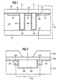
- the light source shown in FIG. 1 has a continuous layer 10 made of a semiconducting material.
- the layer 10 consists, for example, of highly doped polycrystalline silicon. In the case shown, the layer 10 is p + -doped, but it can also be n + -doped.
- the layer 10 contains a dopant such as boron or aluminum in a concentration of preferably approximately 1 x 10 19 cm -3 to 1 x 10 20 cm -3 .
- Layer 20 is doped with a dopant of the opposite conductivity type.
- dopants for layer 20, which may also consist of polycrystalline silicon, in particular, are phosphorus and arsenic.
- the concentration of this dopant is preferably 10 13 cm -3 to 10 19 cm -3 .
- the layer 20 has recesses 30 and 40.
- the Recesses 30 and 40 are perpendicular to a main surface the layer 20 attached and penetrate the layer 20 Completely.
- the layer 20 has highly doped regions 50, 60 and 70 in its upper region, the doping being, for example, a p + doping.
- a membrane layer 75 provided with a plurality of openings. The openings of the membrane layer 75 essentially correspond to the recesses 30 and 40.
- An insulation layer 80 is located above the layer 20 and the membrane layer 75.
- the insulation layer 80 consists of a material that is well insulated electrically and at the same time is transparent in the desired emission range of the light source. In the present case, the insulation layer 80 consists of silicon oxide SiO 2 .
- the insulation layer 80 can be made semi-transparent.
- a semitransparent formation of the insulation layer 80 can be achieved, for example, by adding a dye, for example by means of suitable ions or organic color molecules, or by one or more reflective layers.
- blocker layers 90 and 100 While the recesses 30 and 40 are delimited in their upper region by the insulation layer 80, their further delimitations are formed by blocker layers 90 and 100.
- the blocker layers 90 and 100 can be made of any material that prevents the passage of a medium located in the recesses 30 and 40. However, it is also possible that the blocker layers 90 and 100 also have electrical insulation properties. In order to combine a good blocking effect with a likewise good electrical insulation, in the present case the blocker layers 90 and 100 are formed by conformally deposited silicon oxide SiO 2 .
- the blocker layers 90 and 100 preferably have a thickness of approximately 0.1 ⁇ m to 5 ⁇ m.
- the recess 30 is filled with mercury vapor.
- Applying a voltage turns the mercury vapor stimulated to shine. It sends an UV radiation rich light. In the visible area, only yellow, green and blue, but no red lines broadcast. That so emerging light signal can be shown on a display the yellow color component can be used.
- the other recess 40 is filled with a dye that has fluorescence in the red spectral range.
- the layer 10 is at a contact point 110 with a AC power source 130 connected.
- the highly endowed area 70 is at a contact point 120 with the other pole AC power source 130 connected.
- the AC power source 130 generates an AC voltage in the high frequency range of preferably about 100 kHz to 500 kHz.
- the recess 40 makes it possible for the recess 40 to excite the gas so that it lights up. Similar ones It is possible to add the gas in the cavity 30 to stimulate a glow. Preferably the cavities 30 and 40 controlled differently. This has the advantage that their radiation intensity is independent of each other can be controlled. This makes it, for example possible, the color proportions of the individual in a display Varying points of light.
- the light source shown in FIG. 1 can be manufactured, for example, in the manner shown below.
- a layer 10 is deposited on a semiconductor substrate (not shown) by a suitable deposition method, for example a CVD (Chemical Vapor Deposition) method.
- a further layer 20 is deposited on the layer 10.
- the doping of layers 10 and 20 is achieved in that the dopants are added to the process gas of the CVD process in an amount corresponding to the desired concentration.
- the layer 20 is then covered with a suitable one Etching agents such as EDP (ethylenediamine pyrocatechol) etched.
- EDP is an etchant for an anisotropic etching process.
- the Etch rate difference perpendicular to the crystallographic Areas (100) and (111) is 400. This creates at Deep etching is a characteristic form that is used in the present Case for the desired formation of the deep recesses 30 and 40 leads.
- the etching process stops at the highly doped layer 10.
- a boron doping of layer 10 of at least 7 ⁇ 10 19 cm -3 leads to a decrease in the etching rate of EDP by approximately a factor of 50.
- Conductor tracks for connecting layer 10 and highly doped region 70 are generated by the Layer 10 and region 70 are appropriately structured, so that conductor tracks are formed. This structuring can for example by means of conventional photolithographic process steps take place.
- the electric one Connection of the highly doped region 50 and the region of the Layer 10, which bears against the recess 30, can be on the done the same way.
- a layer with a plurality of openings is placed on the layer 20 Membrane layer 75 applied.
- the openings of the Membrane layer 75 correspond essentially to that Recesses 30 and 40. Then the opening of the Membrane layer 75, which is assigned to the recess 40, with a mask, not shown.
- an insulation layer 80 is applied and flowed over. While a temperature of over 2000 ° C is required to flow SiO 2 , BPSG (boron-phosphorus-silicate glass) can be flowed at temperatures of around 800 - 1100 ° C. As a result, the interior of the recess 30 is covered with the blocker layer 90 and at the same time the recess 30 is covered by an area of the insulation layer 80 lying above it.
- the flow of the insulation material, which serves to fill the recess 30, takes place in a gas atmosphere, the chemical composition of which corresponds to the chemical composition desired for the filling of the recess 30.
- the material forming the insulation layer 80 and the blocker layers 90 and 100 can flow through any desired heating. Such heating is particularly considered when this material has a suitably low melting point, as is the case, for example, with BPSG (boron-phosphorus-silicate glass).
- BPSG boron-phosphorus-silicate glass
- short-term annealing processes which are also called RTA (Rapid Thermal Amnealing), can be carried out in various ways. Examples of such short-term annealing processes can be found, for example, in D. Widmann et al .: Technology of Highly Integrated Circuits, 2nd Edition Berlin; Heidelberg; New York; 1996, especially pp. 38-40.
- CMP chemical mechanical polishing
- the Recess 40 After removing the insulation layer above the Recess 40 in turn becomes an insulation material deposited and also heated so that it is so evaporates that there is a blocker layer 100 and at the same time forms a cover for the recess 40.
- This process takes place in a gas atmosphere, its chemical Composition of the desired chemical composition corresponds to the gas filling of the recess 40. To this It is possible to use the recesses 30 and 40 to fill different gases.
- FIG. 1 Another embodiment of a light source according to the invention is shown in FIG .
- this illustration only shows a single recess 230 in an n-doped semiconductor substrate 220.
- further recesses it is also possible here for further recesses to be arranged in the semiconductor substrate 220.
- the recess 230 preferably extends in a width of 10 ⁇ m to 100 ⁇ m and a height of, for example, 10 ⁇ m to 50 ⁇ m in the semiconductor substrate 220.
- two highly doped regions 250 and 270 are arranged.
- the regions 250 and 270 are, for example, p + -doped, which can be done by implanting boron or aluminum.
- the insulation layer 280 is located on the membrane layer 274.
- the insulation layer 280 is formed, for example, from silicon oxide SiO 2 .
- the bottom and the side surfaces of the recess 230 are separated from the semiconductor substrate 220 by a blocker layer 290.
- Another semiconductor layer 300 which serves as a screen, is located above the insulation layer 280.
- the light source shown in FIG. 2 can be manufactured, for example, in the manner shown below.
- the semiconductor substrate 220 is then coated with a suitable etching agents such as EDP (ethylenediamine pyrocatechol) etched.
- EDP is an etchant for an anisotropic Etching process.
- the etch rate difference perpendicular to the crystallographic areas (100) and (111) is 400. This creates a characteristic during deep etching Form that in the present case to the desired training a deep recess 230 leads.
- the etching process stops inside the semiconductor substrate 220.
- Conductor tracks for connecting the highly doped areas 250 and 270 are generated by regions 250 and 270 be appropriately structured so that there are conductor tracks emerge. This structuring can, for example using conventional photolithographic process steps respectively.
- One is placed on the semiconductor substrate 220 multi-aperture membrane layer 274 applied. The openings of the membrane layer 274 correspond in essentially of the recess 230.
- an insulation layer 280 is applied and flowed over. While a temperature of over 2000.degree. C. is required for the flow of SiO 2 , BPSG (boron-phosphorus-silicate glass) can already be flowed at temperatures of approximately 800-1100 ° C. As a result, the interior of the recess 230 is covered with the blocker layer 290 and at the same time the recess 230 is covered by a region of the insulation layer 280 lying above it.
- the insulation material which serves to close the recess 230 flows in a gas atmosphere whose chemical composition corresponds to the chemical composition desired for filling the recess 230.
- the material forming the insulation layer 280 and the blocker layer 290 can flow through any desired heating. Such heating is particularly considered when this material has a suitably low melting point, as is the case, for example, with BPSG (boron-phosphorus-silicate glass).
- BPSG boron-phosphorus-silicate glass
- short-term annealing processes which are also called RTA (Rapid Thermal Amnealing) can be carried out in various ways. Examples of such short-term annealing processes can be found, for example, in D. Widmann et al .: Technology of Highly Integrated Circuits, 2nd Edition Berlin; Heidelberg; New York; 1996, especially pp. 38-40.
- the invention is in no way from those shown Embodiments limited. In particular, it is possible to exchange the doping types p and n with each other. It is within the scope of the invention to create both light sources which have a single recess, as well as the light source To be designed so that they are a multitude of individual Has recesses. For example, it is possible to an extensive substrate more than 1000 x 1000 to provide individual recesses and thus a high-resolution Creating screen. Depending on the intended use different controls for each individual recess or for groups of recesses. It is particularly expedient that each with some recesses are filled with a gas in a first wavelength emitted while other recesses in one or more Emit wavelengths and thus form other colors. It is already known with conventional screens that with the help of three primary colors, preferably red, green and blue, representing all colors of visible light to let. This principle can of course also be found in a light source according to the invention can be used.
- Another area of application of the light source according to the invention is the formation of inexpensive signal sources for the Use in an integrated optoelectronic circuit.
- the high light intensity makes it suitable Light source according to the invention also for use as a transmitter in a fiber optic network.
Landscapes
- Physics & Mathematics (AREA)
- Electromagnetism (AREA)
- Engineering & Computer Science (AREA)
- Plasma & Fusion (AREA)
- Led Devices (AREA)
Description
- Fig. 1
- einen Querschnitt durch eine erste Ausführungsform einer erfindungsgemäßen Lichtquelle und
- Fig. 2
- einen Querschnitt durch eine zweite Ausführungsform einer erfindungsgemäßen Lichtquelle.
- 10
- Schicht
- 20
- Schicht
- 30
- Ausnehmung
- 40
- Ausnehmung
- 50
- hochdotierter Bereich
- 60
- hochdotierter Bereich
- 70
- hochdotierter Bereich
- 75
- Membranschicht
- 80
- Isolationsschicht
- 90
- Blockerschicht
- 100
- Blockerschicht
- 110
- Kontaktpunkt
- 120
- Kontaktpunkt
- 130
- Wechselstromquelle
- 220
- Halbleitersubstrat
- 230
- Ausnehmung
- 250
- hochdotierter Bereich
- 270
- hochdotierter Bereich
- 274
- Membranschicht
- 280
- Isolationsschicht
- 290
- Blockerschicht
- 300
- Halbleiterschicht
Claims (17)
- Lichtquelle, die wenigstens ein Halbleitermaterial (20; 220) enthält, das wenigstens eine Ausnehmung (30, 40; 230) aufweist, die mit einem Gas oder mit einer Flüssigkeit befüllt ist,
dadurch gekennzeichnet, daß
das Halbleitermaterial (20; 220) in Bereichen, die der Ausnehmung (30, 40; 230) zugewandt sind, mit einer Diffusionsblockerschicht (90, 100; 290) versehen ist, die eine Diffusion des Gases oder der Flüssigkeit in das Halbleitermaterial (20; 220) verhindert. - Lichtquelle nach Anspruch 1,
dadurch gekennzeichnet, daß
die Ausnehmung (30, 40; 230)auf einer Oberfläche durch einen Isolator und auf ihren anderen Oberflächen durch das Halbleitermaterial (20; 220) bedeckt ist. - Lichtquelle nach Anspruch 2,
dadurch gekennzeichnet, daß
der Isolator als eine sich parallel zu einer Oberfläche des Halbleitermaterials (20; 220) erstreckende Isolationsschicht (80; 280) ausgebildet ist. - Lichtquelle nach Anspruch 3,
dadurch gekennzeichnet, daß
die Diffusionsblockerschicht (90, 100; 290) aus einem isolierenden Material besteht. - Lichtquelle nach Anspruch 4,
dadurch gekennzeichnet, daß
die Diffusionsblockerschicht (90, 100; 290) und ein mit der Ausnehmung (30, 40; 230) in Kontakt befindlicher Isolator (80; 280) aus dem gleichen Material bestehen. - Lichtquelle nach Anspruch 4 oder 5,
dadurch gekennzeichnet, daß
die Diffusionsblockerschicht aus Siliziumoxid (SiO2) besteht. - Lichtquelle nach einem der Ansprüche 1 bis 6,
dadurch gekennzeichnet, daß
die Ausnehmung (30, 40; 230) mit einem fluoreszierenden Gas befüllt ist. - Lichtquelle nach Anspruch 7,
dadurch gekennzeichnet, daß
das fluoreszierende Gas wenigstens einen metastabilen Zustand enthält. - Lichtquelle nach Anspruch 8,
dadurch gekennzeichnet, daß
das fluoreszierende Gas Hg-Atome enthält. - Lichtquelle nach Anspruch 9,
dadurch gekennzeichnet, daß
das Gas einen oder mehrere Zusätze aus der Gruppe Tl, Na oder Cd enthält. - Lichtquelle nach einem der Ansprüche 7 bis 10,
dadurch gekennzeichnet, daß
das fluoreszierende Gas Fluor enthält. - Lichtquelle nach einem der Ansprüche 7 bis 11,
dadurch gekennzeichnet, daß
das fluoreszierende Gas wenigstens einen organischen Farbstoff enthält, oder daß das fluoreszierende Gas durch einen organischen Farbstoff gebildet wird. - Lichtquelle nach Anspruch 12,
dadurch gekennzeichnet, daß
der organische Farbstoff Eosin oder Fluorescein enthält. - Lichtquelle nach einem der Ansprüche 7 bis 10,
dadurch gekennzeichnet, daß
das fluoreszierende Gas wenigstens einen aromatischen Kohlenwasserstoff enthält oder aus einem oder mehreren aromatischen Kohlenwasserstoffen besteht. - Lichtquelle nach Anspruch 14,
dadurch gekennzeichnet, daß
der aromatische Kohlenwasserstoff Benzol, Naphthalin oder Anthracen enthält. - Integrierte elektrische Schaltung,
dadurch gekennzeichnet, daß
sie wenigstens eine Lichtquelle nach einem der Ansprüche 1 bis 15 enthält. - Anzeigevorrichtung,
dadurch gekennzeichnet, daß
sie wenigstens eine Lichtquelle nach einem der Ansprüche 1 bis 15 und/oder wenigstens eine integrierte elektrische Schaltung nach Anspruch 16 enthält.
Applications Claiming Priority (3)
| Application Number | Priority Date | Filing Date | Title |
|---|---|---|---|
| DE19802160 | 1998-01-21 | ||
| DE19802160A DE19802160A1 (de) | 1998-01-21 | 1998-01-21 | Lichtquelle und Verfahren zu ihrer Herstellung |
| PCT/DE1999/000006 WO1999038195A1 (de) | 1998-01-21 | 1999-01-04 | Lichtquelle und verfahren zu ihrer herstellung |
Publications (2)
| Publication Number | Publication Date |
|---|---|
| EP1057210A1 EP1057210A1 (de) | 2000-12-06 |
| EP1057210B1 true EP1057210B1 (de) | 2003-02-12 |
Family
ID=7855244
Family Applications (1)
| Application Number | Title | Priority Date | Filing Date |
|---|---|---|---|
| EP99904692A Expired - Lifetime EP1057210B1 (de) | 1998-01-21 | 1999-01-04 | Lichtquelle und verfahren zu ihrer herstellung |
Country Status (4)
| Country | Link |
|---|---|
| EP (1) | EP1057210B1 (de) |
| DE (2) | DE19802160A1 (de) |
| TW (1) | TW409431B (de) |
| WO (1) | WO1999038195A1 (de) |
Family Cites Families (8)
| Publication number | Priority date | Publication date | Assignee | Title |
|---|---|---|---|---|
| DE2903102A1 (de) * | 1979-01-27 | 1980-07-31 | Dahlberg Reinhard | Elektronisches bauelement |
| KR920001844B1 (ko) * | 1986-07-15 | 1992-03-05 | 티디 케이 가부시기가이샤 | 냉음극형 방전 등 장치 |
| US5493177A (en) * | 1990-12-03 | 1996-02-20 | The Regents Of The University Of California | Sealed micromachined vacuum and gas filled devices |
| JPH05135743A (ja) * | 1991-11-11 | 1993-06-01 | Yokogawa Electric Corp | 微小ガス放電素子 |
| EP0581376A1 (de) * | 1992-07-28 | 1994-02-02 | Koninklijke Philips Electronics N.V. | Gastentladungslampe und Verfahren zur Herstellung derselben mittels Mikro-Bearbeitungstechnologie |
| DE4232743A1 (de) * | 1992-09-30 | 1994-03-31 | Wolfgang Dipl Ing Topf | Energiesparende Lichtquelle in Modulform |
| GB2284703A (en) * | 1993-12-11 | 1995-06-14 | Smiths Industries Plc | Discharge lamp |
| DE19734650B4 (de) * | 1997-08-07 | 2007-06-21 | Fraunhofer-Gesellschaft zur Förderung der angewandten Forschung e.V. | Vorrichtung zur Emission elektromagnetischer Strahlung durch Gasentladung, Verfahren zu ihrer Herstellung und Verwendung der Vorrichtung |
-
1998
- 1998-01-21 DE DE19802160A patent/DE19802160A1/de not_active Withdrawn
-
1999
- 1999-01-04 EP EP99904692A patent/EP1057210B1/de not_active Expired - Lifetime
- 1999-01-04 DE DE59904273T patent/DE59904273D1/de not_active Expired - Lifetime
- 1999-01-04 WO PCT/DE1999/000006 patent/WO1999038195A1/de not_active Ceased
- 1999-01-07 TW TW088100189A patent/TW409431B/zh not_active IP Right Cessation
Also Published As
| Publication number | Publication date |
|---|---|
| WO1999038195A1 (de) | 1999-07-29 |
| TW409431B (en) | 2000-10-21 |
| EP1057210A1 (de) | 2000-12-06 |
| DE19802160A1 (de) | 1999-07-22 |
| DE59904273D1 (de) | 2003-03-20 |
Similar Documents
| Publication | Publication Date | Title |
|---|---|---|
| DE69836177T2 (de) | Lichtemittierende Halbleitervorrichtung, die Nanokristalle enthält | |
| DE69735022T2 (de) | Verfahren zur Herstellung einer Matrixanzeigevorrichtung | |
| DE3688231T2 (de) | Dynamische speichervorrichtung mit wahlfreiem zugriff mit einem monokristallinen transistor auf einer rillenartigen kondensatorstruktur und herstellungsverfahren dafuer. | |
| WO2018077957A1 (de) | Verfahren zur herstellung von optoelektronischen halbleiterbauteilen und optoelektronisches halbleiterbauteil | |
| DE3633311A1 (de) | Elektrolumineszenzvorrichtung | |
| DE3841588A1 (de) | Dynamischer vertikal-halbleiterspeicher mit wahlfreiem zugriff und verfahren zu seiner herstellung | |
| EP0010596A1 (de) | Verfahren zur Ausbildung von Maskenöffnungen bei der Herstellung von Halbleiteranordnungen | |
| DE69414898T2 (de) | Licht emittierende Vorrichtung und Verfahren zu ihrer Herstellung | |
| DE19808168A1 (de) | Halbleitereinrichtung und Verfahren zur Herstellung derselben | |
| EP0645808A1 (de) | Verfahren zur Herstellung eines Isolationsgrabens in einem SOI-Substrat | |
| DE69820184T2 (de) | Lichtemittierendes Halbleiterbauelement und Verfahren zu dessen Herstellung | |
| DE4428195C1 (de) | Verfahren zur Herstellung eines Siliziumkondensators | |
| DE2943435A1 (de) | Halbleiterelement und verfahren zu dessen herstellung | |
| WO2018234154A1 (de) | Optoelektronisches halbleiterbauelement | |
| DE102013101051B4 (de) | Plasmazelle und Verfahren zur Herstellung einer Plasmazelle | |
| DE19954867C1 (de) | DRAM-Zellenanordnung und Verfahren zu deren Herstellung | |
| EP1129482B1 (de) | Verfahren zur Herstellung von einer DRAM-Zellenanordnung | |
| DE4418430C1 (de) | Verfahren zur Herstellung eines Siliziumkondensators | |
| DE102013211707A1 (de) | Anordnung mit einem Träger | |
| WO2020182621A1 (de) | Verfahren zur herstellung von optoelektronischen halbleiterbauteilen und optoelektronisches halbleiterbauteil | |
| DE2601652C3 (de) | Verfahren zur epitaxialen Abscheidung einer Am. Bv Halbleiterschicht auf einem Germaniumsubstrat mit einer (100)-Orientierong | |
| DE19802160A1 (de) | Lichtquelle und Verfahren zu ihrer Herstellung | |
| DE4035402A1 (de) | Integrierter halbleiterlaser mit unterschiedlichen wellenlaengen und verfahren zum herstellen eines solchen lasers | |
| DE2162219A1 (de) | Verfahren zum Herstellen eines Feldeffekttransistors | |
| DE19821999A1 (de) | SOI-Halbleiteranordnung und Verfahren zur Herstellung derselben |
Legal Events
| Date | Code | Title | Description |
|---|---|---|---|
| PUAI | Public reference made under article 153(3) epc to a published international application that has entered the european phase |
Free format text: ORIGINAL CODE: 0009012 |
|
| 17P | Request for examination filed |
Effective date: 20000713 |
|
| AK | Designated contracting states |
Kind code of ref document: A1 Designated state(s): DE |
|
| 17Q | First examination report despatched |
Effective date: 20010521 |
|
| GRAG | Despatch of communication of intention to grant |
Free format text: ORIGINAL CODE: EPIDOS AGRA |
|
| GRAG | Despatch of communication of intention to grant |
Free format text: ORIGINAL CODE: EPIDOS AGRA |
|
| GRAH | Despatch of communication of intention to grant a patent |
Free format text: ORIGINAL CODE: EPIDOS IGRA |
|
| GRAH | Despatch of communication of intention to grant a patent |
Free format text: ORIGINAL CODE: EPIDOS IGRA |
|
| GRAA | (expected) grant |
Free format text: ORIGINAL CODE: 0009210 |
|
| AK | Designated contracting states |
Designated state(s): DE |
|
| REF | Corresponds to: |
Ref document number: 59904273 Country of ref document: DE Date of ref document: 20030320 Kind code of ref document: P |
|
| PLBE | No opposition filed within time limit |
Free format text: ORIGINAL CODE: 0009261 |
|
| STAA | Information on the status of an ep patent application or granted ep patent |
Free format text: STATUS: NO OPPOSITION FILED WITHIN TIME LIMIT |
|
| 26N | No opposition filed |
Effective date: 20031113 |
|
| PGFP | Annual fee paid to national office [announced via postgrant information from national office to epo] |
Ref country code: DE Payment date: 20180727 Year of fee payment: 20 |
|
| REG | Reference to a national code |
Ref country code: DE Ref legal event code: R071 Ref document number: 59904273 Country of ref document: DE |