EP1050094B1 - Supply of power to primary conductors - Google Patents
Supply of power to primary conductors Download PDFInfo
- Publication number
- EP1050094B1 EP1050094B1 EP98962726A EP98962726A EP1050094B1 EP 1050094 B1 EP1050094 B1 EP 1050094B1 EP 98962726 A EP98962726 A EP 98962726A EP 98962726 A EP98962726 A EP 98962726A EP 1050094 B1 EP1050094 B1 EP 1050094B1
- Authority
- EP
- European Patent Office
- Prior art keywords
- network
- trackway
- primary
- transconductance
- current
- Prior art date
- Legal status (The legal status is an assumption and is not a legal conclusion. Google has not performed a legal analysis and makes no representation as to the accuracy of the status listed.)
- Revoked
Links
- 239000004020 conductor Substances 0.000 title claims description 21
- 230000001939 inductive effect Effects 0.000 claims description 48
- 239000003990 capacitor Substances 0.000 claims description 22
- 238000012546 transfer Methods 0.000 claims description 22
- 230000008878 coupling Effects 0.000 claims description 5
- 238000010168 coupling process Methods 0.000 claims description 5
- 238000005859 coupling reaction Methods 0.000 claims description 5
- 230000005293 ferrimagnetic effect Effects 0.000 claims description 5
- 230000005294 ferromagnetic effect Effects 0.000 claims description 3
- 229910000859 α-Fe Inorganic materials 0.000 claims 2
- 230000000694 effects Effects 0.000 claims 1
- 230000001747 exhibiting effect Effects 0.000 claims 1
- 238000010586 diagram Methods 0.000 description 16
- 230000008901 benefit Effects 0.000 description 11
- 230000037361 pathway Effects 0.000 description 11
- 238000000034 method Methods 0.000 description 10
- 238000013461 design Methods 0.000 description 9
- 238000009434 installation Methods 0.000 description 5
- 230000008859 change Effects 0.000 description 4
- 230000004907 flux Effects 0.000 description 4
- 230000009471 action Effects 0.000 description 3
- 230000005291 magnetic effect Effects 0.000 description 3
- 230000005855 radiation Effects 0.000 description 3
- 238000001816 cooling Methods 0.000 description 2
- 230000001419 dependent effect Effects 0.000 description 2
- 230000009467 reduction Effects 0.000 description 2
- 230000007704 transition Effects 0.000 description 2
- 238000004804 winding Methods 0.000 description 2
- 101100451260 Arabidopsis thaliana HMGS gene Proteins 0.000 description 1
- 230000002411 adverse Effects 0.000 description 1
- 230000004075 alteration Effects 0.000 description 1
- XAGFODPZIPBFFR-UHFFFAOYSA-N aluminium Chemical compound [Al] XAGFODPZIPBFFR-UHFFFAOYSA-N 0.000 description 1
- 229910052782 aluminium Inorganic materials 0.000 description 1
- 239000004411 aluminium Substances 0.000 description 1
- 230000001174 ascending effect Effects 0.000 description 1
- 230000000295 complement effect Effects 0.000 description 1
- 238000010276 construction Methods 0.000 description 1
- 238000012937 correction Methods 0.000 description 1
- 238000011161 development Methods 0.000 description 1
- 230000018109 developmental process Effects 0.000 description 1
- 230000002500 effect on skin Effects 0.000 description 1
- 238000005516 engineering process Methods 0.000 description 1
- 238000009413 insulation Methods 0.000 description 1
- 239000000463 material Substances 0.000 description 1
- 238000012986 modification Methods 0.000 description 1
- 230000004048 modification Effects 0.000 description 1
- 238000013021 overheating Methods 0.000 description 1
- 238000000079 presaturation Methods 0.000 description 1
- 230000008569 process Effects 0.000 description 1
- 230000003252 repetitive effect Effects 0.000 description 1
- 238000010561 standard procedure Methods 0.000 description 1
- 238000012795 verification Methods 0.000 description 1
Images

Classifications
-
- H—ELECTRICITY
- H02—GENERATION; CONVERSION OR DISTRIBUTION OF ELECTRIC POWER
- H02J—CIRCUIT ARRANGEMENTS OR SYSTEMS FOR SUPPLYING OR DISTRIBUTING ELECTRIC POWER; SYSTEMS FOR STORING ELECTRIC ENERGY
- H02J3/00—Circuit arrangements for ac mains or ac distribution networks
- H02J3/04—Circuit arrangements for ac mains or ac distribution networks for connecting networks of the same frequency but supplied from different sources
- H02J3/06—Controlling transfer of power between connected networks; Controlling sharing of load between connected networks
-
- H—ELECTRICITY
- H04—ELECTRIC COMMUNICATION TECHNIQUE
- H04B—TRANSMISSION
- H04B5/00—Near-field transmission systems, e.g. inductive or capacitive transmission systems
-
- H—ELECTRICITY
- H02—GENERATION; CONVERSION OR DISTRIBUTION OF ELECTRIC POWER
- H02J—CIRCUIT ARRANGEMENTS OR SYSTEMS FOR SUPPLYING OR DISTRIBUTING ELECTRIC POWER; SYSTEMS FOR STORING ELECTRIC ENERGY
- H02J7/00—Circuit arrangements for charging or depolarising batteries or for supplying loads from batteries
- H02J7/0029—Circuit arrangements for charging or depolarising batteries or for supplying loads from batteries with safety or protection devices or circuits
- H02J7/00309—Overheat or overtemperature protection
-
- H—ELECTRICITY
- H02—GENERATION; CONVERSION OR DISTRIBUTION OF ELECTRIC POWER
- H02J—CIRCUIT ARRANGEMENTS OR SYSTEMS FOR SUPPLYING OR DISTRIBUTING ELECTRIC POWER; SYSTEMS FOR STORING ELECTRIC ENERGY
- H02J50/00—Circuit arrangements or systems for wireless supply or distribution of electric power
- H02J50/10—Circuit arrangements or systems for wireless supply or distribution of electric power using inductive coupling
- H02J50/12—Circuit arrangements or systems for wireless supply or distribution of electric power using inductive coupling of the resonant type
-
- H—ELECTRICITY
- H02—GENERATION; CONVERSION OR DISTRIBUTION OF ELECTRIC POWER
- H02J—CIRCUIT ARRANGEMENTS OR SYSTEMS FOR SUPPLYING OR DISTRIBUTING ELECTRIC POWER; SYSTEMS FOR STORING ELECTRIC ENERGY
- H02J50/00—Circuit arrangements or systems for wireless supply or distribution of electric power
- H02J50/40—Circuit arrangements or systems for wireless supply or distribution of electric power using two or more transmitting or receiving devices
- H02J50/402—Circuit arrangements or systems for wireless supply or distribution of electric power using two or more transmitting or receiving devices the two or more transmitting or the two or more receiving devices being integrated in the same unit, e.g. power mats with several coils or antennas with several sub-antennas
-
- H—ELECTRICITY
- H01—ELECTRIC ELEMENTS
- H01F—MAGNETS; INDUCTANCES; TRANSFORMERS; SELECTION OF MATERIALS FOR THEIR MAGNETIC PROPERTIES
- H01F17/00—Fixed inductances of the signal type
- H01F17/04—Fixed inductances of the signal type with magnetic core
- H01F17/06—Fixed inductances of the signal type with magnetic core with core substantially closed in itself, e.g. toroid
-
- H—ELECTRICITY
- H01—ELECTRIC ELEMENTS
- H01F—MAGNETS; INDUCTANCES; TRANSFORMERS; SELECTION OF MATERIALS FOR THEIR MAGNETIC PROPERTIES
- H01F3/00—Cores, Yokes, or armatures
- H01F3/10—Composite arrangements of magnetic circuits
- H01F3/14—Constrictions; Gaps, e.g. air-gaps
-
- H—ELECTRICITY
- H02—GENERATION; CONVERSION OR DISTRIBUTION OF ELECTRIC POWER
- H02J—CIRCUIT ARRANGEMENTS OR SYSTEMS FOR SUPPLYING OR DISTRIBUTING ELECTRIC POWER; SYSTEMS FOR STORING ELECTRIC ENERGY
- H02J50/00—Circuit arrangements or systems for wireless supply or distribution of electric power
- H02J50/005—Mechanical details of housing or structure aiming to accommodate the power transfer means, e.g. mechanical integration of coils, antennas or transducers into emitting or receiving devices
-
- H—ELECTRICITY
- H02—GENERATION; CONVERSION OR DISTRIBUTION OF ELECTRIC POWER
- H02J—CIRCUIT ARRANGEMENTS OR SYSTEMS FOR SUPPLYING OR DISTRIBUTING ELECTRIC POWER; SYSTEMS FOR STORING ELECTRIC ENERGY
- H02J50/00—Circuit arrangements or systems for wireless supply or distribution of electric power
- H02J50/70—Circuit arrangements or systems for wireless supply or distribution of electric power involving the reduction of electric, magnetic or electromagnetic leakage fields
-
- H—ELECTRICITY
- H04—ELECTRIC COMMUNICATION TECHNIQUE
- H04B—TRANSMISSION
- H04B5/00—Near-field transmission systems, e.g. inductive or capacitive transmission systems
- H04B5/20—Near-field transmission systems, e.g. inductive or capacitive transmission systems characterised by the transmission technique; characterised by the transmission medium
- H04B5/22—Capacitive coupling
-
- H—ELECTRICITY
- H04—ELECTRIC COMMUNICATION TECHNIQUE
- H04B—TRANSMISSION
- H04B5/00—Near-field transmission systems, e.g. inductive or capacitive transmission systems
- H04B5/70—Near-field transmission systems, e.g. inductive or capacitive transmission systems specially adapted for specific purposes
- H04B5/79—Near-field transmission systems, e.g. inductive or capacitive transmission systems specially adapted for specific purposes for data transfer in combination with power transfer
Definitions
- This invention relates to the supply of power to the trackway conductors forming the primary circuit of an inductive power supply system; in particular this invention relates to the supply of power to the trackway conductors connected in a series resonant circuit which comprises the primary circuit of an inductive power supply system capable of distributing inductive power over a distance.
- An inductive power transfer system generally comprises (a) a generator of alternating current, (b) one or more conductors carrying the alternating current as tracks (the "primary inductive pathway") to one or more consumers, (c) a space carrying an alternating magnetic flux as a consequence of current flow within the conductor(s), (d) a pickup means (the “secondary winding"), which intercepts a part of the magnetic flux, and (e) power consuming means.
- Track extension methods are not suitable for parallel tuned tracks because when the track length is increased the "group velocity" of the track tends to zero while the characteristic impedance at the required frequency tends to infinity.
- series compensated tracks can be extended using "modules” including lumped series capacitors, without adding to the number of system poles.
- Previous techniques for generating AC resonant currents in inductive power transfer have generally been optimised for the case of parallel-tuned circuits.
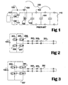
- An example high-frequency converter (see Fig 1 ) has a half-bridge configuration.
- the action of the switches can be regarded simply as adding boosts to the resonating current, like maintaining a child's movements on a swing.
- the switches generally change state at or very close to a zero-voltage condition and switching losses are thereby minimised.
- the resonating capacitance is generally a lumped capacitance within or close to the power supply, and the track inductance comprises most of the resonating inductance.
- the current in the track is a relatively pure sine wave.
- This type of converter is described for example in our Application No: PCT/GB92/01463 . It can be regarded as a "half-bridge" converter, where a centre-tapped inductor having a high reactance forms a passive half of a bridge and provides a DC return path.
- This type of converter is generally used in a "slave" mode in that its switching frequency is determined by the actual resonant frequency of the system.
- the particular converter that we have selected is quite efficient, has low switching losses, and the switches themselves do not carry the magnetising current of the track. However it does have a propensity to detuning and having an unstable frequency under heavy loads, and the energy stored in the DC inductor may cause a voltage and/or current overshoot if the load is reduced suddenly.
- a series compensated track for use in inductive power transfer systems may be described as an elongated conductive loop wherein the outgoing and return conductors are parallel and spaced apart.
- the inductive reactance is maintained at or near a relatively small value despite extensions of length, by inserting sets of discrete capacitors in series with the conductors at one or more evenly spaced sites.
- One example "small value" of inductance is 620 ⁇ H-in relation to a track energised at 15 kHz, resistance 0.4 ohms, circulating current 250 A, at I kV rms.
- US 55046608 discloses an apparatus for providing power from an alternating power source.
- WO 93/23909 discloses a primary inductive track or path for a resonant inductive power distribution system made up from a number of modules each supplied as a pre-built and substantially pre-tuned segment of the track.
- the invention provides a method for removing the current from a primary inductive pathway fed from a trans-pi network, wherein the method comprises shorting the primary inductive pathway at or near the point of feed.
- the invention provides a method for varying the current circulating within a primary inductive pathway fed from more than one network, wherein the method comprises controllable addition of the outputs from each of the more than one network into the primary inductive pathway.
- This application particularly relates to a series-compensated primary trackway, in which the conductors include lumped series capacitances as appropriate for maintaining the system-wide resonant frequency at or near a desired value.
- Advantages of the series-compensated design include:
- This example comprises a full-bridge switching circuit in which each arm of the bridge is occupied by a switch and no resonating components exist within the circuit.
- a circuit illustrating the principle is the illustrated in Fig 2 .
- switches are insulated-gate base transistors (IGBTs) and operating frequency is generally at about 10 kHz, although IGBT devices are becoming increasingly capable of high-speed operation.
- the series resonant track is indicated at 201 and comprises a series of series capacitors 202, in series with track inductance 203 (here the track inductance is shown as a lumped symbol).
- each of the four switches (204, 205, 206, 207) is operated in a 180 degree conduction angle, and current passes alternately from a DC supply 105 through 204, then through the track, then 207, or from the DC supply though 205, through the track in the opposite direction, and then 206, to reach the DC return path.
- Diodes e.g. 205 absorb switching transients. There are likely to be significant switching losses in this circuit, in which the switches are usually not opened or closed at zero-voltage instants.
- Fig 4 indicates the waveforms to be expected in this type of circuit.
- 401 is the gate drive to one set of switches (e.g. 204 and 207) and 402 is the drive to the diagonally opposite set (e.g. 205 and 206).
- Waveform 403 shows the resulting current supplied to the series resonant track or primary conductor 201 (with (lumped) inductance 203 and interspersed series capacitances 202). Because the odd harmonics in the initially square waveform see a greater inductance than does the fundamental component, the current waveform within the track tends to become comparatively sinusoidal.
- Vn 4 ⁇ E DC ⁇ n ⁇ 2 ⁇ sin n ⁇ 2
- Vn is the output voltage
- ⁇ is the phase angle between a reference drive signal and a second drive signal
- E DC is the DC supply voltage
- V3 the third harmonic
- the first remaining harmonic is the fifth.
- the small drop in voltage supplied is tolerable for the sake of nulling out the third harmonic.
- the prior-art half-bridge resonant converter of Fig 1 could easily be controlled so as to switch at each zero-voltage instant - a feature which minimises switching losses and the generation of interference.
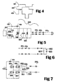
- the circuit of Fig 2 assumed that zero-voltage switching was not intended. We have found that if the circuit of Fig 2 is driven at a frequency slightly above the resonant frequency of the track and if we also include a small capacitor 301 across each switching device, as shown in Fig 3 , it is then possible to take advantage of the inductive impedance of the track in order to attain zero-voltage switching. A residual track inductance discharges the parallel capacitors during switching transitions.
- the small capacitors are each of the order of 100 to 1000 nF (example capacitor used at 15 kHz - where switches are 300A, 1200V IGBTs are WIMA 0.22 ⁇ F FKP1).
- the "lock-out" time between switching the top and bottom transistors has to be controlled and the knowledge that the turn-off time of a practical solid-state switch is longer than the turn-on time should be included in a design.
- full-bridge converters described above have some control advantages, they also suffer from the significant drawback that the full circulating current passes through the switching devices. If a half-bridge power supply could be modified so that it can provide current to a series-compensated track, one would expect that the switching devices would be much more lightly loaded. Furthermore the drive current provided by the previous example is relatively rich in harmonics. Even though the higher harmonics see a higher impedance, at least part of those higher harmonics are radiated.
- the circuit 500 drives a series resonant primary inductive loop 20; including lumped capacitors 202 and distributed (track) inductances 203 from a half-bridge pair of switches 502, 503 using an internal resonant circuit comprising an inductor 505 and capacitor 504 as a resonant circuit across which the loop is connected.
- the values of the components may be entirely determined so that resonance at the intended frequency is achieved without reference to the loading track, or the values may allow for the inductance and capacitance presented by the track.
- the remainder of the circuit 500 is similar to that of Fig 1 ; a controller 501 drives the gates of a pair of IGBT devices in a complementary way.
- a DC splitter inductor 106 having a high reactance at the operating frequency towards a negative potential.
- the centre tap of inductor 106 is fed with a constant current (as a result of inductor 104) from a voltage source 105.
- This circuit comprises a current sourced half-bridge supply.
- the current carried by the switches is only that required to "top up" the circulating resonant current, and that the primary trackway 201 is supplied with a close approximation to a sine wave. Because the devices are switched at zero-voltage instants, transients are minimised and the devices can be used at their full ratings, subject of course to the usual frequency of operation derating.
- the switching devices are supplying the "topping-up" current and are switched at zero-voltage instants and so the current rating can be perhaps 1/4 to 1/6 the current rating of those in a full bridge.
- Control of circulating current in the primary pathway if required, can be exercised through variations in the DC power fed to the half-bridge circuit.
- the frequency of the switching currents can be held constant by an autonomous frequency source or can "float" at a switching rate dependent on the overall system resonant frequency (unless, as with Fig 2 or Fig 3 , one is trying to accomplish zero-voltage switching by using a slightly higher than resonant rate).
- This figure shows the termination apparatus for a series-compensated track. If the track (including a repetitive series of inductance and capacitance 203, 202) was simply terminated by a short circuit (a wire of zero impedance) then the harmonics present in the current produced by the power supply no longer see a short-circuited track but a modified reactive impedance, depending on the electrical length of the track at the harmonic frequency. For example if the electrical length is a quarter wavelength then it will appear to be an open circuit at the input and the harmonic content will be altered.
- the preferred termination apparatus is intended to act as a proper termination for all harmonics.
- the impedance 601 is a resistive, frequency-independent impedance, having a value set by reference to the characteristic impedance of the track, and the values of components in the series resonant circuit comprised of inductor 602 and capacitor 603 are chosen to resonate, at the resonant frequency and so present a short circuit.
- the termination apparatus tends to define the magnitude of currents at frequencies other than resonance.
- the least harmonic content is realised when using a power supply including a dedicated parallel resonant circuit such as in Fig 5 and a termination as per fig 6 . Under these circumstances the amount of wasted power through radiation (hence minimal radio frequency interference) or through stray coupling is minimised. Loss of power through being unavailable to a tuned resonant pickup device in also minimised, and yet the advantages of a series compensated track are still available.
- This figure shows a configuration for a full bridge power supply including a parallel resonant circuit or tank circuit; a configuration which provides many of the advantages of Example 3.
- capacitor 701 with inductor 702 are selected so as to be capable of resonance at the intended operating frequency. Of course, a significant amount of circulating current will flow in these components.
- Switching devices 204, 205, 206, and 207 form a full bridge capable of exciting the resonant circuit by alternately connecting one end or the other of capacitor 701 to high or low voltages.
- 202 refers to the start of a series compensated primary conductor loop or trackway as illustrated elsewhere.
- Current to the full bridge is supplied as a constant-current source via inductor 104 from DC source 105.
- the inductor 104 provides voltage-compliant supply rails and also reduces the return of switching transients into the supply of power - typically a mains supply.
- FIG 8 illustrates the general concept of "intentional mis-matching".
- a series-compensated trackway (804) appears as substantially a zero impedance, while the inductance/capacitance network (802 with 803), resonant at the operating frequency, appears to the trackway to be an infinite impedance.
- Supplying a zero impedance load from an infinite impedance source results in a constant current circulating within the track.
- a power source 801 driving the system via a resonant circuit comprising inductance 802 and capacitance 803 will see an impedance which is (a) not zero, and (b) not purely resistive.
- This concept assumes that any load placed on the trackway is substantially a pure resistance - that is - a resonant circuit which has been tuned reasonably close to that of the primary trackway.
- the alternating-current source 801 preferred for use in this example is a voltage source and preferably produces a sine wave voltage or a reasonable approximation to a sine wave, at a constant, predetermined frequency. However these requirements can be varied.
- Fig 9 develops Fig 8 into a first version of a transconductance pi ("trans-pi") network for matching a source of current to a series-resonant inductive power transfer trackway 804.
- 901 and 902 form a tuned circuit that is generally a part of the power source.
- 903 is a capacitor which was originally determined to serve as a power factor correction capacitor, chosen so that the input resistance to the pi network when driving a purely resistive load is itself purely resistive, so that the frequency of the tuned circuit is constant. Surprisingly, this value is the same as that providing resonance at the operating frequency in conjunction with the inductor 904.
- the capacitor (-j4) should have a capacitative reactance of 4 ohms, as should the capacitor 905.
- the group of parallel-resonant components, 903, 904, and 905 comprises this version of the transconductance pi ("trans-pi") network.
- the well-known pi coupling network used in radio transmitters to match an aerial load to an output stage is series-resonant.
- Fig 10 shows a simplified circuit diagram of a more preferred means for matching a source of power to an inductive power transfer trackway, using a transconductance pi ("trans-pi") network.
- the inductance 904 of Fig 9 is split into a symmetrical pair, one in each leg (1004 with 1004').
- One advantage is that currents within the inductive pathway 1005 are balanced and less radio interference is caused.
- Each inductor is now of reactance j2, not j4 as in Fig 9 .
- trans-pi transconductance pi
- capacitors 903 and 905 each of example capacitative reactance 4 ohms
- inductances 1004 and 1004' each of example inductive reactance of 2 ohms.
- the current handling capacity should of course be adequate to handle the circulating current which we term the "bias current” as distinct from the "track current".
- the track current will be about half of the bias current; regardless of track impedance which typically ranges from 1 to 8 ohms.
- the inductive reactance of would be about 21 ⁇ H, in a practical system running at 15 kHz, with a supply voltage of 500V, a bias current of 500A, and a track current of 250 A.
- this predetermining process for setting a track current assumes a constant voltage source. If the voltage can change, then currents in various trackways will change in proportion.
- trans-pi network can act as a voltage converter. Should the track impedance be greater than the values of reactance used in the network, then the output voltage will be greater than the input, and it is possible to drive a track with several kilovolts output from a trans-pi network while driving that network with a lower, semiconductor-compatible voltage such as 800-1000 volts. This allows a longer length of trackway to be driven.
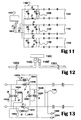
- Fig 11 shows a simplified circuit diagram including several inductive power transfer trackways, using a single power supply (1101) and a separate trans-pi network (as per the example contained within the box 1105) for each branch. This is a "star" configuration. Because it is possible to switch off the current within a particular branch (any one of 1102, 1103, or 1104) by closing a corresponding shorting switch (1106, 1107, or 1108), a system designer can design a system in which all of the power from one power supply can be fed into any one individual trackway (1102, 1103, or 1104). Alternatively, the power can be shared between several trackways by opening more than one switch at a time. Even if all trackways were shorted, the power supply would not be adversely affected.
- the current circulating in a particular trackway may be preset. This may be useful if for example certain trackways in a system are used for purposes other than inductive pathways for moving vehicles, but instead have less demanding devices such as battery charging outlets connected to them.
- a policy of loss reduction may be implemented in a practical system; by reducing the track current to 0.7, losses are halved.
- trackway 1104 in Fig 11 has the different reactances of 3 ohms for the inductances and 6 ohms for the capacitances. This results in a circulating current that is 66.7% that of the other two trackways 1102 and 1103, which use reactances of 2 ohms for the inductances and 4 ohms for the capacitances.
- This type of circuit can be applied in a "retail interface", where members of the public purchase power from an inductively transferred pathway. Once the consumer's account has been entered and verified (presumably by some electronic means), current can be permitted to flow by action of a "verification controller” on the appropriate switch, and can then be transferred to the consumer. This might be used in road transport or for battery charging.
- Fig 12 shows a simplified circuit diagram for a method that doubles the length of an inductive power transfer trackway that can be fed by a single power supply. The procedure depends on the possibility of de-energising an individual trackway by shorting it, without affecting the power supply or other trackways also drawing current from the same supply.
- a single power supply 1101 drives a pair of units 1105, 1105' each like the one contained within the dashed box 1105 of Fig 11 . Each unit also includes a shorting switch, like 1106 in Fig 11 .
- an elongated primary trackway (note: series compensation capacitors not shown) made up of two halves 1201 and 1202, which are brought close together at the region of the power supply/trans-pi networks, at approximately the middle of the elongated trackway.
- Some form of vehicle proximity detector may be used to determine whether there is a device capable of drawing power located on either half of the trackway and if there is, the corresponding shorting switch 1106 is opened and the trackway is energised, so supplying the consumer. No power is wasted by energising a trackway which cannot feed a power consumer at the time.
- vehicle proximity detector might comprise weakly energising the trackway and detecting a load; otherwise active sensors, perhaps independent of connection to the trackway conductors could be used.
- trackway may also be used to refer to power cabling for use in lighting installations, such as fluorescent lighting installations.
- Fig 13 we show further means for controlling the circulating current within a trackway by switching component values within the trans-pi network. It is possible to employ groups of components instead of single parts, switching in different combinations in order to vary the track current. For example, as shown in Fig 13 , one could decrease inductance from j3 to j6 (by adding parallel inductors 1301A, 1301D across inductors 1301B, 1301C, and at the same time adding parallel capacitance 1302B and 1302D across 1302A and 1302C to go from j-3 to j-6 and, while retaining the condition of resonance, cut the losses to half whenever full power is not required.
- zero current is obtained by shorting the output of the trans-pi network regardless of whether it is switched to operate in the second or third modes described below.
- this switch is one having mercury-wetted contacts so that minimal internal resistance exists, but a solid-state switch alternative may be more reliable and faster in action, for example so that zero-crossing switching can be realised.
- Control line 1305 controls this switch.
- a low track current is obtained by using higher inductance and lower capacitance values within the trans-pi network, while maintaining resonance.
- a high track current is obtained by using lower inductance and higher capacitance values within the trans-pi network, again while maintaining resonance.
- adding inductance and adding capacitance both in parallel across existing components and closing a suitable type of remotely controlled switch affecting control line 1304 to make the connection results in a transition from the second mode to the third mode.
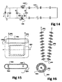
- Fig 14 shows how apparatus and a method may be provided for immediately and passively controlling the current circulating within a trans-pi network should a fault develop, for example if the track 1401 becomes an open circuit. If this happens, the current circulating within the network tends towards infinity.
- saturable inductors having a ferrimagnetic (or ferromagnetic) core.
- Fig 14 shows 1402 and 1403 as two saturable inductors.
- the resonant frequency of the network will change away from the pre-saturation value of j2 as indicated and so it will work less effectively with power generated at a defined frequency.
- Saturation is a bulk property of materials and is fast and be fully reliable. It is desirable to back this protection up with some form of power supply turning-off protection in case continued saturation leads to overheating.
- Fig 15 shows a physical design 1500 for one type of inductor that could be used with a 250 to 500 kW supply.
- An inductor of appropriate reactance is comprised of about 10 metres of litz wire 1505 capable of carrying a bias current of about 500 A, formed into a loop of four turns held within an aluminium container 1502 to act as an electrical shield by means of the generation of eddy currents within the inner surface of the box.
- the section 1501 at A-A shows how a preferred box would be approximately equidistantly spaced apart from the conductor(s) 1505.
- the cables comprising the inductance would be clamped ( fixing means 1506) so that the windings remain in approximately the centre of the space inside the box 1501. Some cooling apertures would normally be required.
- Connectors 1503 and 1504 are for electrical connection of the cable to the remainder of the circuit. A box of this type could be hung from the rear of a cabinet holding the remainder of the circuitry.
- Fig 16 shows another version of the inductor.
- a single hanging loop 1605 of litz wire passes through a number of ferrimagnetic-cored inductances 1603 each being in this example a "C" shaped interrupted toroid.
- the core raises the inductance of the single turn (perhaps one metre) of wire; provides a saturable component, and also restricts the emergence of magnetic flux from the wire.
- a shielding box (not shown) is still preferred for containing leaked flux, and for safety and protection.
- the cores will become heated through hysteresis during use, and convection or forced cooling may be required.
- a single toroid-like core 1603 is shown in section below, with the conductor 1602 within and a gap 1604 in which the energy is stored.
- the cost of this design may be less than that for Fig 15a; if toroids are cheaper than a sufficient amount of litz wire rated to carry 500 A.
- the cores may be mounted by means of the gap, and the position of the rather flexible cable is thereby controlled.
- the construction of capacitor units for use in a 250 to 500 kW trans-pi unit is a standard procedure.
- This invention covers several aspects of the supply of power to the trackway conductors forming the primary circuit of an inductive power supply system.
- advantages include:
- advantages include:
Landscapes
- Engineering & Computer Science (AREA)
- Power Engineering (AREA)
- Computer Networks & Wireless Communication (AREA)
- Signal Processing (AREA)
- Inverter Devices (AREA)
Description
- This invention relates to the supply of power to the trackway conductors forming the primary circuit of an inductive power supply system; in particular this invention relates to the supply of power to the trackway conductors connected in a series resonant circuit which comprises the primary circuit of an inductive power supply system capable of distributing inductive power over a distance.
- An inductive power transfer system generally comprises (a) a generator of alternating current, (b) one or more conductors carrying the alternating current as tracks (the "primary inductive pathway") to one or more consumers, (c) a space carrying an alternating magnetic flux as a consequence of current flow within the conductor(s), (d) a pickup means (the "secondary winding"), which intercepts a part of the magnetic flux, and (e) power consuming means. Systems originating from our developments have been characterised by inclusion of: (f) an operating frequency generally above 10 kHz, (g) a tuned, resonant primary and a tuned, resonant secondary, (h) loose coupling between primary and secondary, and (i) provide power control by means of partial decoupling of the secondary without significantly affecting other consumers sharing the same primary conductors.
- We first developed parallel tuned primary inductive pathways for inductive power transfer. When inductive power transfer is to be applied to systems including relatively long primary inductive pathways or tracks, high-frequency alternating currents at the high voltage that is required to drive parallel-tuned tracks become rather difficult to generate in a practicable manner. The high voltage is required in order to insert sufficient current into the track, given an unavoidable track inductance. It is difficult to drive a long, parallel-tuned track because (apart from safety and insulation considerations) there are finite limits to the voltage that can be switched, and handled, using known technology. Furthermore, safety is a real issue. Track extension methods are not suitable for parallel tuned tracks because when the track length is increased the "group velocity" of the track tends to zero while the characteristic impedance at the required frequency tends to infinity. In contrast, series compensated tracks can be extended using "modules" including lumped series capacitors, without adding to the number of system poles.
- Previous techniques for generating AC resonant currents in inductive power transfer have generally been optimised for the case of parallel-tuned circuits. An example high-frequency converter (see
Fig 1 ) has a half-bridge configuration. The action of the switches can be regarded simply as adding boosts to the resonating current, like maintaining a child's movements on a swing. Usefully, the switches generally change state at or very close to a zero-voltage condition and switching losses are thereby minimised. In our preferred version, the resonating capacitance is generally a lumped capacitance within or close to the power supply, and the track inductance comprises most of the resonating inductance. The current in the track is a relatively pure sine wave. This type of converter is described for example in our Application No:PCT/GB92/01463 - Now that the advantages of series compensated tracks (as defined later) are becoming evident, and series compensated tracks are seen as being more relevant to commercialisation of inductive power transfer, other types of power supply may be preferable.
- Furthermore, for possible applications such as the provision of inductive power to rail vehicles, there is a need to raise the amount of current that can be fed into a given track, and to raise the distance over which that current can be effective, and in general there is a need for reduction of the capital costs associated with an installation.
- A series compensated track for use in inductive power transfer systems may be described as an elongated conductive loop wherein the outgoing and return conductors are parallel and spaced apart. During installation the inductive reactance is maintained at or near a relatively small value despite extensions of length, by inserting sets of discrete capacitors in series with the conductors at one or more evenly spaced sites. One example "small value" of inductance is 620 µH-in relation to a track energised at 15 kHz, resistance 0.4 ohms, circulating current 250 A, at I kV rms.
-
US 55046608 WO 93/23909 - It is an object of this invention to provide improved means for energising an inductive power transfer system, or at least to provide the public with a useful choice.
- According to the present invention there is provided an apparatus as claimed in
claim 1. - Preferred embodiments are described in the dependent claims.
- In yet another related aspect the invention provides a method for removing the current from a primary inductive pathway fed from a trans-pi network, wherein the method comprises shorting the primary inductive pathway at or near the point of feed.
- In a yet further related aspect the invention provides a method for varying the current circulating within a primary inductive pathway fed from more than one network, wherein the method comprises controllable addition of the outputs from each of the more than one network into the primary inductive pathway.
- The preferred embodiments to be described and illustrated in this specification are provided purely by way of example and are in no way intended to be limiting as to the spirit or the scope of the invention.
-
Fig 1 : shows a simplified circuit diagram of a prior-art half-bridge converter, according to the prior art, and a further prior-art parallel-tuned track. -
Fig 2 : shows a simplified circuit diagram of examplary full-bridge converter, for providing current to a series-compensated track. -
Fig 3 : shows a simplified circuit diagram of a full-bridge converter, including capacitors wired between the emitter and the collector of each IGBT for assisting in obtaining a zero-voltage switching mode. -
Fig 4 : shows a simplified circuit diagram of waveforms associated with a full-bridge converter. -
Fig 5 : shows a simplified circuit diagram of a half-bridge converter including a resonant circuit for providing currents to a series-compensated track. -
Fig 6 : shows a simplified circuit diagram of means for termination of a series-compensated track. -
Fig 7 : shows a simplified circuit diagram of a full-bridge converter including a resonant circuit and joined to a series-compensated track. -
Fig 8 : shows a simplified circuit diagram showing the origination of a transconductance pi ("trans-pi") network for matching a source of power to an inductive power transfer trackway. Note: letters such as "j2", "-j6" in following drawings indicate inductive or capacitative impedances (for example, "j2" = an inductive reactance of 2 ohms and for a 15 kHz system, j2 is equivalent to 21 µH). -
Fig 9 : shows a simplified circuit diagram of a preferred means for matching a source of power to an inductive power transfer trackway, using a trans-pi network. -
Fig 10 : shows a simplified circuit diagram of a more practical means for matching a source of power to an inductive power transfer trackway, using a trans-pi network. -
Fig 11 : shows a simplified circuit diagram of an inductive power transfer system layout, using a single power supply and one transconductance pi ("trans-pi") network for each branch. -
Fig 12 : shows a simplified circuit diagram for providing power to a long inductive trackway, such as a railway or road, by splitting the trackway and providing means to feed either half (as required) through a trans-pi network, both halves being supplied from a single power supply. -
Fig 13 : shows apparatus for providing zero, a low, and a high value of circulating current within a trackway, by means of switches. -
Fig 14 : shows apparatus for limiting the value of circulating current within a trans-pi filter (as may happen if the trackway becomes an open circuit), by means of one or more saturable inductors. -
Fig 15 : shows a preferred design for an inductance suitable for use in a trans-pi filter at power levels of around 250 kW. -
Fig 16 : shows another preferred design for an inductance having a core and suitable for use in a trans-pi filter at power levels of around 250 kW. - Parallel-tuned trackways (as shown in the prior art
Fig 1 ) are not practicable for long-distance distribution of inductively transferred power, in part because the voltage requirements for inserting current into a track will quickly reach the limits of safety and of component ratings. (103 represents the inductance of the straight primary conductors and 101 represents the capacitance between them, while 102 is a lumped capacitor which serves to tune the trackway to the system frequency). - This application particularly relates to a series-compensated primary trackway, in which the conductors include lumped series capacitances as appropriate for maintaining the system-wide resonant frequency at or near a desired value. Advantages of the series-compensated design include:
- 1) A substantially constant impedance is seen by the power supply, regardless of length, so that voltage requirements remain feasible.
- 2) Because there are no additional system poles, the resonant frequency is stable. For example, there are no ties linking various nodes of the track, and because the whole track is one resonant circuit, different modes of resonance do not occur.
- 3) Of course resistive (skin-effect) losses and radiation, for example, will eventually limit the feasible length of series-compensated primary trackways.
- This example comprises a full-bridge switching circuit in which each arm of the bridge is occupied by a switch and no resonating components exist within the circuit. A circuit illustrating the principle is the illustrated in
Fig 2 . switches are insulated-gate base transistors (IGBTs) and operating frequency is generally at about 10 kHz, although IGBT devices are becoming increasingly capable of high-speed operation. The series resonant track is indicated at 201 and comprises a series ofseries capacitors 202, in series with track inductance 203 (here the track inductance is shown as a lumped symbol). - In the simple form at least, each of the four switches (204, 205, 206, 207) is operated in a 180 degree conduction angle, and current passes alternately from a
DC supply 105 through 204, then through the track, then 207, or from the DC supply though 205, through the track in the opposite direction, and then 206, to reach the DC return path. Diodes (e.g. 205) absorb switching transients. There are likely to be significant switching losses in this circuit, in which the switches are usually not opened or closed at zero-voltage instants. -
Fig 4 indicates the waveforms to be expected in this type of circuit. 401 is the gate drive to one set of switches (e.g. 204 and 207) and 402 is the drive to the diagonally opposite set (e.g. 205 and 206).Waveform 403 shows the resulting current supplied to the series resonant track or primary conductor 201 (with (lumped)inductance 203 and interspersed series capacitances 202). Because the odd harmonics in the initially square waveform see a greater inductance than does the fundamental component, the current waveform within the track tends to become comparatively sinusoidal. - In order to control track current, one can either vary the voltage of the DC source, or vary the phase of the drive signals to the switches, relative to one reference drive signal, so that as the phase α is varied between 0 and 180 degrees, the output voltage (of the fundamental) ranges between zero and about 90% of the DC supply.
- The relationship (for the nth harmonic) is given by:

where Vn is the output voltage,
α is the phase angle between a reference drive signal and a second drive signal, and EDC is the DC supply voltage. - It follows that if α is made 120 degrees, then V3 (the third harmonic) is zero, and the first remaining harmonic is the fifth. The small drop in voltage supplied is tolerable for the sake of nulling out the third harmonic.
- The prior-art half-bridge resonant converter of
Fig 1 could easily be controlled so as to switch at each zero-voltage instant - a feature which minimises switching losses and the generation of interference. The circuit ofFig 2 assumed that zero-voltage switching was not intended. We have found that if the circuit ofFig 2 is driven at a frequency slightly above the resonant frequency of the track and if we also include asmall capacitor 301 across each switching device, as shown inFig 3 , it is then possible to take advantage of the inductive impedance of the track in order to attain zero-voltage switching. A residual track inductance discharges the parallel capacitors during switching transitions. The small capacitors are each of the order of 100 to 1000 nF (example capacitor used at 15 kHz - where switches are 300A, 1200V IGBTs are WIMA 0.22 µF FKP1). Of course the "lock-out" time between switching the top and bottom transistors has to be controlled and the knowledge that the turn-off time of a practical solid-state switch is longer than the turn-on time should be included in a design. - While the full-bridge converters described above have some control advantages, they also suffer from the significant drawback that the full circulating current passes through the switching devices. If a half-bridge power supply could be modified so that it can provide current to a series-compensated track, one would expect that the switching devices would be much more lightly loaded. Furthermore the drive current provided by the previous example is relatively rich in harmonics. Even though the higher harmonics see a higher impedance, at least part of those higher harmonics are radiated.
- In
Fig 5 , thecircuit 500 drives a series resonant primary inductive loop 20; including lumpedcapacitors 202 and distributed (track)inductances 203 from a half-bridge pair ofswitches inductor 505 andcapacitor 504 as a resonant circuit across which the loop is connected. The values of the components may be entirely determined so that resonance at the intended frequency is achieved without reference to the loading track, or the values may allow for the inductance and capacitance presented by the track. The remainder of thecircuit 500 is similar to that ofFig 1 ; acontroller 501 drives the gates of a pair of IGBT devices in a complementary way. These devices pull first one side, then the other, of aDC splitter inductor 106 having a high reactance at the operating frequency towards a negative potential. The centre tap ofinductor 106 is fed with a constant current (as a result of inductor 104) from avoltage source 105. This circuit comprises a current sourced half-bridge supply. - Advantages of this circuit include that the current carried by the switches is only that required to "top up" the circulating resonant current, and that the
primary trackway 201 is supplied with a close approximation to a sine wave. Because the devices are switched at zero-voltage instants, transients are minimised and the devices can be used at their full ratings, subject of course to the usual frequency of operation derating. - In a full bridge circuit lacking a resonant tank circuit (for example;
figs 2 or 3 ), the switching devices must carry the full circulating current, and must be derated for the high-frequency usage (because they are not switched at zero-voltage instants). Although IGBT devices are now being produced that can switch heavy currents at say 15 kHz, they are relatively expensive. If the primary track has a Q of 3.0, and if the frequency derating factor is taken as 2, then switches rated as being capable of switching 6 times the drawn-off current are needed for circuits corresponding to Examples 1 and 2. In contrast, in a half-bridge circuit the switching devices are supplying the "topping-up" current and are switched at zero-voltage instants and so the current rating can be perhaps 1/4 to 1/6 the current rating of those in a full bridge. Control of circulating current in the primary pathway, if required, can be exercised through variations in the DC power fed to the half-bridge circuit. - In either case the frequency of the switching currents can be held constant by an autonomous frequency source or can "float" at a switching rate dependent on the overall system resonant frequency (unless, as with
Fig 2 or Fig 3 , one is trying to accomplish zero-voltage switching by using a slightly higher than resonant rate). - This figure shows the termination apparatus for a series-compensated track. If the track (including a repetitive series of inductance and
capacitance 203, 202) was simply terminated by a short circuit (a wire of zero impedance) then the harmonics present in the current produced by the power supply no longer see a short-circuited track but a modified reactive impedance, depending on the electrical length of the track at the harmonic frequency. For example if the electrical length is a quarter wavelength then it will appear to be an open circuit at the input and the harmonic content will be altered. The preferred termination apparatus is intended to act as a proper termination for all harmonics. Theimpedance 601 is a resistive, frequency-independent impedance, having a value set by reference to the characteristic impedance of the track, and the values of components in the series resonant circuit comprised ofinductor 602 andcapacitor 603 are chosen to resonate, at the resonant frequency and so present a short circuit. Thus the termination apparatus tends to define the magnitude of currents at frequencies other than resonance. - The least harmonic content is realised when using a power supply including a dedicated parallel resonant circuit such as in
Fig 5 and a termination as perfig 6 . Under these circumstances the amount of wasted power through radiation (hence minimal radio frequency interference) or through stray coupling is minimised. Loss of power through being unavailable to a tuned resonant pickup device in also minimised, and yet the advantages of a series compensated track are still available. - This figure shows a configuration for a full bridge power supply including a parallel resonant circuit or tank circuit; a configuration which provides many of the advantages of Example 3. In this circuit,
capacitor 701 withinductor 702 are selected so as to be capable of resonance at the intended operating frequency. Of course, a significant amount of circulating current will flow in these components.Switching devices capacitor 701 to high or low voltages. 202 refers to the start of a series compensated primary conductor loop or trackway as illustrated elsewhere. Current to the full bridge is supplied as a constant-current source viainductor 104 fromDC source 105. Theinductor 104 provides voltage-compliant supply rails and also reduces the return of switching transients into the supply of power - typically a mains supply. - The simplified circuit diagram,
Fig 8 , illustrates the general concept of "intentional mis-matching". A series-compensated trackway (804) appears as substantially a zero impedance, while the inductance/capacitance network (802 with 803), resonant at the operating frequency, appears to the trackway to be an infinite impedance. Supplying a zero impedance load from an infinite impedance source results in a constant current circulating within the track. Meanwhile apower source 801 driving the system via a resonantcircuit comprising inductance 802 andcapacitance 803 will see an impedance which is (a) not zero, and (b) not purely resistive. This concept assumes that any load placed on the trackway is substantially a pure resistance - that is - a resonant circuit which has been tuned reasonably close to that of the primary trackway. - The alternating-
current source 801 preferred for use in this example is a voltage source and preferably produces a sine wave voltage or a reasonable approximation to a sine wave, at a constant, predetermined frequency. However these requirements can be varied. -
Fig 9 developsFig 8 into a first version of a transconductance pi ("trans-pi") network for matching a source of current to a series-resonant inductivepower transfer trackway 804. 901 and 902 form a tuned circuit that is generally a part of the power source. 903 is a capacitor which was originally determined to serve as a power factor correction capacitor, chosen so that the input resistance to the pi network when driving a purely resistive load is itself purely resistive, so that the frequency of the tuned circuit is constant. Surprisingly, this value is the same as that providing resonance at the operating frequency in conjunction with theinductor 904. For example, if the inductor 904 (j4) has an inductive reactance of 4 ohms, the capacitor (-j4) should have a capacitative reactance of 4 ohms, as should thecapacitor 905. The group of parallel-resonant components, 903, 904, and 905 comprises this version of the transconductance pi ("trans-pi") network. In comparison, the well-known pi coupling network used in radio transmitters to match an aerial load to an output stage is series-resonant. -
Fig 10 shows a simplified circuit diagram of a more preferred means for matching a source of power to an inductive power transfer trackway, using a transconductance pi ("trans-pi") network. Here, theinductance 904 ofFig 9 is split into a symmetrical pair, one in each leg (1004 with 1004'). One advantage is that currents within the inductive pathway 1005 are balanced and less radio interference is caused. Each inductor is now of reactance j2, not j4 as inFig 9 . Thus the preferred transconductance pi ("trans-pi") network of this invention comprises (infig 10 )capacitors 903 and 905 (each ofexample capacitative reactance 4 ohms), together withinductances 1004 and 1004' (each of example inductive reactance of 2 ohms). - The current handling capacity should of course be adequate to handle the circulating current which we term the "bias current" as distinct from the "track current". For a 1000 V supply, use of a set of resonant components of reactances j2, -j2 will result in a bias current of 1000/j2 = 500A. Typically the track current will be about half of the bias current; regardless of track impedance which typically ranges from 1 to 8 ohms. The inductive reactance of would be about 21 µH, in a practical system running at 15 kHz, with a supply voltage of 500V, a bias current of 500A, and a track current of 250 A. Of course this predetermining process for setting a track current assumes a constant voltage source. If the voltage can change, then currents in various trackways will change in proportion.
- One of the advantages of using a trans-pi network with its inherent mismatch is that it can act as a voltage converter. Should the track impedance be greater than the values of reactance used in the network, then the output voltage will be greater than the input, and it is possible to drive a track with several kilovolts output from a trans-pi network while driving that network with a lower, semiconductor-compatible voltage such as 800-1000 volts. This allows a longer length of trackway to be driven.
-
Fig 11 shows a simplified circuit diagram including several inductive power transfer trackways, using a single power supply (1101) and a separate trans-pi network (as per the example contained within the box 1105) for each branch. This is a "star" configuration. Because it is possible to switch off the current within a particular branch (any one of 1102, 1103, or 1104) by closing a corresponding shorting switch (1106, 1107, or 1108), a system designer can design a system in which all of the power from one power supply can be fed into any one individual trackway (1102, 1103, or 1104). Alternatively, the power can be shared between several trackways by opening more than one switch at a time. Even if all trackways were shorted, the power supply would not be adversely affected. Furthermore, by predetermining the value of the components of the trans-pi network, as shown for the network supplying thetrackway 1104, the current circulating in a particular trackway may be preset. This may be useful if for example certain trackways in a system are used for purposes other than inductive pathways for moving vehicles, but instead have less demanding devices such as battery charging outlets connected to them. - A policy of loss reduction may be implemented in a practical system; by reducing the track current to 0.7, losses are halved. For example, note that
trackway 1104 inFig 11 has the different reactances of 3 ohms for the inductances and 6 ohms for the capacitances. This results in a circulating current that is 66.7% that of the other twotrackways - This type of circuit can be applied in a "retail interface", where members of the public purchase power from an inductively transferred pathway. Once the consumer's account has been entered and verified (presumably by some electronic means), current can be permitted to flow by action of a "verification controller" on the appropriate switch, and can then be transferred to the consumer. This might be used in road transport or for battery charging.
-
Fig 12 : shows a simplified circuit diagram for a method that doubles the length of an inductive power transfer trackway that can be fed by a single power supply. The procedure depends on the possibility of de-energising an individual trackway by shorting it, without affecting the power supply or other trackways also drawing current from the same supply. Asingle power supply 1101 drives a pair ofunits 1105, 1105' each like the one contained within the dashedbox 1105 ofFig 11 . Each unit also includes a shorting switch, like 1106 inFig 11 . There is an elongated primary trackway (note: series compensation capacitors not shown) made up of twohalves switch 1106 is opened and the trackway is energised, so supplying the consumer. No power is wasted by energising a trackway which cannot feed a power consumer at the time. One form of vehicle proximity detector might comprise weakly energising the trackway and detecting a load; otherwise active sensors, perhaps independent of connection to the trackway conductors could be used. The term "trackway" may also be used to refer to power cabling for use in lighting installations, such as fluorescent lighting installations. - In
Fig 13 we show further means for controlling the circulating current within a trackway by switching component values within the trans-pi network. It is possible to employ groups of components instead of single parts, switching in different combinations in order to vary the track current. For example, as shown inFig 13 , one could decrease inductance from j3 to j6 (by addingparallel inductors parallel capacitance - In a first operating mode, zero current is obtained by shorting the output of the trans-pi network regardless of whether it is switched to operate in the second or third modes described below. Preferably this switch is one having mercury-wetted contacts so that minimal internal resistance exists, but a solid-state switch alternative may be more reliable and faster in action, for example so that zero-crossing switching can be realised.
Control line 1305 controls this switch. - In a second mode, a low track current is obtained by using higher inductance and lower capacitance values within the trans-pi network, while maintaining resonance.
- In a third mode, a high track current is obtained by using lower inductance and higher capacitance values within the trans-pi network, again while maintaining resonance. Conveniently, adding inductance and adding capacitance both in parallel across existing components and closing a suitable type of remotely controlled switch affecting
control line 1304 to make the connection results in a transition from the second mode to the third mode.Fig 14 shows how apparatus and a method may be provided for immediately and passively controlling the current circulating within a trans-pi network should a fault develop, for example if thetrack 1401 becomes an open circuit. If this happens, the current circulating within the network tends towards infinity. In order to limit the maximum amount of current we prefer to provide saturable inductors having a ferrimagnetic (or ferromagnetic) core.Fig 14 shows -
Fig 15 shows aphysical design 1500 for one type of inductor that could be used with a 250 to 500 kW supply. An inductor of appropriate reactance is comprised of about 10 metres oflitz wire 1505 capable of carrying a bias current of about 500 A, formed into a loop of four turns held within analuminium container 1502 to act as an electrical shield by means of the generation of eddy currents within the inner surface of the box. Thesection 1501 at A-A, reproduced below, shows how a preferred box would be approximately equidistantly spaced apart from the conductor(s) 1505. The cables comprising the inductance would be clamped ( fixing means 1506) so that the windings remain in approximately the centre of the space inside thebox 1501. Some cooling apertures would normally be required.Connectors -
Fig 16 shows another version of the inductor. Asingle hanging loop 1605 of litz wire passes through a number of ferrimagnetic-coredinductances 1603 each being in this example a "C" shaped interrupted toroid. In practice we might use 50 cores in the descending loop and 50 in the ascending loop. The core raises the inductance of the single turn (perhaps one metre) of wire; provides a saturable component, and also restricts the emergence of magnetic flux from the wire. A shielding box (not shown) is still preferred for containing leaked flux, and for safety and protection. The cores will become heated through hysteresis during use, and convection or forced cooling may be required. A single toroid-like core 1603 is shown in section below, with theconductor 1602 within and agap 1604 in which the energy is stored. The cost of this design may be less than that for Fig 15a; if toroids are cheaper than a sufficient amount of litz wire rated to carry 500 A. The cores may be mounted by means of the gap, and the position of the rather flexible cable is thereby controlled. In general the construction of capacitor units for use in a 250 to 500 kW trans-pi unit is a standard procedure. - This invention covers several aspects of the supply of power to the trackway conductors forming the primary circuit of an inductive power supply system. For the power supply examples without a parallel resonant circuit at the output:
- 1. Zero-voltage switching can be realised, and
- 2. Control of track current can be provided by altering drive impulses.
- For the examples of power supplies including a parallel resonant circuit, advantages include:
- 1. Capable of driving series-compensated inductive power transfer tracks, and is easily scaled up in power.
- 2. Zero-voltage switching is accomplished easily.
- 3. Little or no derating of switches is required at useful frequencies (such as 5, 10, 15 kHz).
- 4. A sine wave voltage (substantially) is supplied to the track; minimising radiation of harmonics.
- For the versions using a "trans-pi" network to supply a series compensated track, advantages include:
- 1. The use of a trans-pi network for coupling many trackways to a single large power supply is generally much more economical than providing one power supply for each trackway. A design for a complex system of conveyers perhaps including hundreds of individual powered vehicles in a factory should then be cheaper, because the provision of many relatively small power supplies tends to become the most expensive part of the installation. In such complex systems, battery charging means, conveyer lifts and sideways transfer devices may also be installed, and can also be supplied by inductive power transfer.
- 2. Trackways can be supplied with more, or less current by varying trans-pi component reactances; for example so that a roadway inductive power transfer system receives more current during rush traffic on one side (or the other) of a roadway. At other times losses can be reduced by supplying less current.
- 3. An elongated trackway can be fed at a higher voltage than can feasibly be generated by present-day devices by tailoring the reactances within the trans-pi network to the impedance of the trackway, so allowing longer distances of inductively powered transportation per power supply unit.
- 4. An elongated trackway can be fed centrally, using trans-pi net works as per
Fig 12 , so that long-distance inductively powered transportation requires (for this example) only half the number of power supplies per unit length of track (the maximum energisable length). - 5. Saturable inductors may provide "front-line" protection from open circuit faults in the trackway.
- Finally, it will be appreciated that various alterations and modifications may be made to the foregoing without departing from the scope of this invention as set forth in the following claims.
Claims (14)
- An apparatus comprising an alternating power source (801) and primary conductors (804) of an inductive power transfer system supply, wherein the power source supplies power to the primary conductors (804) of an inductive power transfer system, said system having at least one tuned primary trackway (804); each of the at least one tuned primary trackway (804) having an inherent resonant frequency, said apparatus further comprises at least one reactive network (903, 904, 905) having an input and an output; wherein said network comprises at least one inductance (904) connected to at least one capacitance (903, 905) said network affecting a transfer of power between the alternating power source and the at least one primary trackway (804), characterised in that the value of said inductance (904) and the value of said capacitance (903, 905) are selected such that the network provides a deliberately mis-matched coupling between the alternating power source (801) and the primary trackway (804) so that the source appears to present a substantially infinite impedance and the primary trackway (804) appears to present a substantially zero impedance; and so that the voltage at the output of the reactive network (903, 904, 905) may in use be substantially greater than that provided to the input of the reactive network (903, 904, 905).
- Apparatus as claimed in claim 1, characterised in that at least one reactive network comprises a transconductance pi network (903, 904, 905) including one or more inductors (904) and one or more capacitors (903, 905), so that the voltage at the output of the transconductance pi network (903, 904, 905) may in use be substantially greater than that provided to the input of the transconductance pi network.
- Apparatus as claimed in claim 2, characterised in that the component values within any one transconductance pi network (903. 904, 905) are selected so that the reactive network is capable of determining the proportion of circulating current to be fed from the output of the reactive network into the primary trackway and so that the amount of circulating current within the primary trackway can be controlled.
- Apparatus as claimed in claim 3, characterised in that each at least one transconductance pi network (903, 904, 905) is connected to a corresponding primary trackway, the transconductance pi network or networks being capable by means of a selection of suitable component values of determining the proportion of circulating current that may be fed from the transconductance pi network into each primary trackway so that the amount of circulating current within the primary trackway can be controlled.
- Apparatus is claimed in claim 4, characterised in that the apparatus comprises more than one transconductance pi network each connected through controllable switching means to one primary trackway, so that the amount of circulating current within the primary trackway can be controlled by connection of the outputs of one or more transconductance pi networks at any time to the primary trackway
- Apparatus as claimed in claim 4, characterised in that the apparatus comprises at least one transconductance pi network (903, 904, 905) connected to each primary trackway (804), the at least one reactive network being provided with at least one set of additional reactive components (1301A, 1301B, 1301C, 1301D) capable as a group of being controllably switched into or out of the network from a first set of components capable of determining a first current, to a second set of components, capable of determining a second current, so that the circulating current to be supplied from the output of the reactive network into each primary trackway can be controlled from time to time and so that the amount of circulating current within the primary trackway (804) can be controlled.
- Apparatus as claimed in claim 2, characterised in that the apparatus provides switching means (1006-1008) across the primary conductors of a primary trackways (804) at a position where any one transconductance pl network (903. 904, 905) is connected to the primary trackway; the switching means being capable when In a closed state of shorting the primary trackway (804) so that the amount of circulating current within the primary trackway (804) falls, and so that the primary trackway is In effect disconnected from the power supply yet the power supply itself does not experience a short-cirouited output
- Apparatus as claimed in claim 2, charactersed in that the one or more of the inductive components of any one transconductance pi network are selected so that the one or more inductive components are capable of entering a state of saturation If a current greater than an intended current should flow through the saturable inductor, so that the circulating current within the primary trackway can be limited.
- Apparatus as claimed In claim 1 having more than one primary trackway (804), characterised in that each primary trackway forms a part of an extended primary trackway; an end of each primary trackway meeting an the end of at least one other primary trackway near the alternating power source (801); each primary trackway being fed at the connection point by a separate transconductance pi network (1105, 1105') having a switching means (1106, 1107) connected across the output of the transconductance pl network, so that in use any primary trackway may be energised in response to the presence of a consumer of inductive power upon that primary trackway by opening the corresponding switching means, so that the power supply output may be directed down a selected section of the primary trackway and limitations of trackway length based on power supply capacity are substantially overcome.
- An inductor suitable for use with apparatus including a transconductance pl network as claimed in claim 6 or in claim 7, characterised in that the inductor is provided with a ferrimagnetic or ferromagnetic core (1402, 1403) capable of saturation at an intended level of current, so that the total circulating current within the network may be limited.
- An inductor suitable for use with a transconductance pl network as claimed in claim 6 or in claim 7, characterised in that more than one turn of litz wire (1505) is held within a conductive container (1501) and apart from the inner surface of the container.
- An inductor suitable for use with a transconductance pi network as claimed in claim 6 or in claim 7 characterised in that the inductor is provided with a ferrimagnetic core (1402, 1403) including one or more toroidal ferrite elements (1603) each interrupted by an air gap and the ferrimagnetic core (1402, 1403) is threaded onto about one turn of litz wire (1602).
- An inductor as claimed in claim 12 characterised in that the one or more ferrite elements are each mounted by means of a support occupying the air gap.
- Apparatus as claimed in claim 1, further characterised in that the apparatus includes termination apparatus; the termination apparatus being connected between an end of one conductor and an end of the other conductor at a position remote from a connection to a power supply, the termination apparatus comprising in parallel connection a resistance capable of exhibiting the characteristic impendance of the track at substantially any frequency, and a series tuned resonant circuit tuned to the inherent resonant frequency; the termination apparatus being capable at the resonant frequency of presenting a short circuit to the track and capable of presenting the characteristic impedance to the track at other frequencies, so that the harmonic content of the current circulating in the track is reduced.
Applications Claiming Priority (5)
| Application Number | Priority Date | Filing Date | Title |
|---|---|---|---|
| NZ32934097A NZ329340A (en) | 1997-12-05 | 1997-12-05 | Supply of AC power to inductive power transfer track via reactive tank circuits |
| NZ32934097 | 1997-12-05 | ||
| NZ32999198 | 1998-03-18 | ||
| NZ32999198 | 1998-03-18 | ||
| PCT/NZ1998/000179 WO1999030402A1 (en) | 1997-12-05 | 1998-12-04 | Supply of power to primary conductors |
Publications (3)
| Publication Number | Publication Date |
|---|---|
| EP1050094A1 EP1050094A1 (en) | 2000-11-08 |
| EP1050094A4 EP1050094A4 (en) | 2005-09-28 |
| EP1050094B1 true EP1050094B1 (en) | 2010-08-04 |
Family
ID=26651863
Family Applications (1)
| Application Number | Title | Priority Date | Filing Date |
|---|---|---|---|
| EP98962726A Revoked EP1050094B1 (en) | 1997-12-05 | 1998-12-04 | Supply of power to primary conductors |
Country Status (8)
| Country | Link |
|---|---|
| US (1) | US6621183B1 (en) |
| EP (1) | EP1050094B1 (en) |
| JP (1) | JP2001526517A (en) |
| KR (1) | KR20010032834A (en) |
| AU (1) | AU1789899A (en) |
| DE (1) | DE69841810D1 (en) |
| TW (1) | TW416172B (en) |
| WO (1) | WO1999030402A1 (en) |
Cited By (4)
| Publication number | Priority date | Publication date | Assignee | Title |
|---|---|---|---|---|
| US8360216B2 (en) | 2008-07-04 | 2013-01-29 | Bombardier Transportation Gmbh | System and method for transferring electric energy to a vehicle |
| US8544622B2 (en) | 2008-09-19 | 2013-10-01 | Bombardier Transportation Gmbh | Producing electromagnetic fields for transferring electric energy to a vehicle |
| US8590682B2 (en) | 2008-07-04 | 2013-11-26 | Bombardier Transportation Gmbh | Transferring electric energy to a vehicle |
| US8827058B2 (en) | 2008-09-19 | 2014-09-09 | Bombardier Transportation Gmbh | Inductively receiving electric energy for a vehicle |
Families Citing this family (39)
| Publication number | Priority date | Publication date | Assignee | Title |
|---|---|---|---|---|
| EP1287608A1 (en) * | 2000-04-03 | 2003-03-05 | Aalborg University | A resonant converter |
| JP2002118988A (en) * | 2000-10-04 | 2002-04-19 | Shinko Electric Co Ltd | Non-contact feeding device |
| JP4671515B2 (en) * | 2001-03-07 | 2011-04-20 | 株式会社椿本チエイン | Power supply device |
| JP4715040B2 (en) * | 2001-06-08 | 2011-07-06 | 富士電機システムズ株式会社 | Semiconductor device |
| US20080108372A1 (en) * | 2002-06-11 | 2008-05-08 | Intelligent Technologies International, Inc. | Inductively Powered Asset Monitoring System |
| NZ525219A (en) * | 2003-04-09 | 2005-11-25 | Auckland Uniservices Ltd | Switchably decoupling resonant circuits utilised for controlling inductive power transfer from an alternating current source |
| NZ526109A (en) * | 2003-05-26 | 2006-09-29 | Auckland Uniservices Ltd | Parallel-tuned pick-up system with multiple voltage outputs |
| JP4192775B2 (en) * | 2003-12-05 | 2008-12-10 | 株式会社ダイフク | Contactless power supply equipment |
| WO2006118473A1 (en) * | 2005-04-29 | 2006-11-09 | Auckland Uniservices Limited | Compensation apparatus and methods for a primary conductive path of an icpt system |
| GB0716679D0 (en) | 2007-08-28 | 2007-10-03 | Fells J | Inductive power supply |
| JP5217324B2 (en) * | 2007-09-14 | 2013-06-19 | シンフォニアテクノロジー株式会社 | Power supply system |
| JP5480483B2 (en) * | 2008-09-22 | 2014-04-23 | パナソニック株式会社 | Non-contact power feeding device |
| US9032880B2 (en) | 2009-01-23 | 2015-05-19 | Magnemotion, Inc. | Transport system powered by short block linear synchronous motors and switching mechanism |
| US8967051B2 (en) | 2009-01-23 | 2015-03-03 | Magnemotion, Inc. | Transport system powered by short block linear synchronous motors and switching mechanism |
| US8616134B2 (en) | 2009-01-23 | 2013-12-31 | Magnemotion, Inc. | Transport system powered by short block linear synchronous motors |
| EP2417686A1 (en) | 2009-04-08 | 2012-02-15 | Access Business Group International LLC | Selectable coil array |
| JP4894894B2 (en) * | 2009-07-22 | 2012-03-14 | Tdk株式会社 | Wireless power supply apparatus and wireless power transmission system |
| DE102009042127A1 (en) * | 2009-09-18 | 2011-03-24 | Siemens Aktiengesellschaft | Inductive conductor for non-contact power transmission and its use for vehicles |
| WO2011046453A1 (en) * | 2009-10-12 | 2011-04-21 | Auckland Uniservices Limited | Inductively controlled series resonant ac power transfer |
| KR101229935B1 (en) * | 2010-07-21 | 2013-02-06 | 한국과학기술원 | Variable inductance compensation device for cross segment power supply line |
| KR101668925B1 (en) | 2011-06-07 | 2016-10-24 | 마그네모션, 인코포레이티드 | Versatile control of a linear synchronous motor propulsion system |
| GB2491651A (en) | 2011-06-10 | 2012-12-12 | Bombardier Transp Gmbh | System and Method for Transferring Electric Energy to a Vehicle Using Constant Current Operation of Segments of a Conductor Arrangement at resonance frequency |
| GB2491652A (en) | 2011-06-10 | 2012-12-12 | Bombardier Transp Gmbh | System and Method for Transferring Electric Energy to a Vehicle Using a Plurality of Segments of a Conductor Arrangement |
| GB201110273D0 (en) * | 2011-06-17 | 2011-08-03 | Isis Innovation | Magneto-inductive waveguide |
| KR101186569B1 (en) | 2011-08-18 | 2012-10-10 | 한국철도기술연구원 | System for charging electric vehicle of railway station using power feed line |
| EP2660948A3 (en) | 2012-05-04 | 2015-06-24 | DET International Holding Limited | Multiple resonant cells for inductive charging pads |
| GB2507533A (en) * | 2012-11-02 | 2014-05-07 | Bombardier Transp Gmbh | Inductive power receiver having compensating arrangement |
| WO2015042409A1 (en) | 2013-09-21 | 2015-03-26 | Magnemotion, Inc. | Linear motor transport for packaging and other uses |
| GB2518650A (en) * | 2013-09-27 | 2015-04-01 | Bombardier Transp Gmbh | Circuit arrangement and method for designing a circuit arrangement of a system for inductive power transfer |
| US9979315B2 (en) | 2013-11-15 | 2018-05-22 | Mitsubishi Electric Engineering Company, Limited | Rectifying circuit for high-frequency power supply |
| US9742200B2 (en) | 2013-12-09 | 2017-08-22 | Qualcomm Incorporated | System and method to avoid magnetic power loss while providing alternating current through a ferromagnetic material |
| US9276413B1 (en) * | 2014-09-25 | 2016-03-01 | Navitas Semiconductor, Inc. | Soft switched single stage wireless power transfer |
| GB2533367A (en) | 2014-12-18 | 2016-06-22 | Bombardier Transp Gmbh | A device and method for adjusting an inductance of an electric conductor |
| US10046659B2 (en) * | 2014-12-19 | 2018-08-14 | Qualcomm Incorporated | Systems, apparatus and method for adaptive wireless power transfer |
| US11165372B2 (en) * | 2017-09-13 | 2021-11-02 | Rockwell Automation Technologies, Inc. | Method and apparatus to characterize loads in a linear synchronous motor system |
| JP7086467B2 (en) * | 2018-04-09 | 2022-06-20 | 日本無線株式会社 | Rail-type non-contact power transmission system |
| US11207988B2 (en) | 2018-08-06 | 2021-12-28 | Robert M. Lyden | Electric or hybrid vehicle with wireless device and method of supplying electromagnetic energy to vehicle |
| US10840707B2 (en) | 2018-08-06 | 2020-11-17 | Robert M. Lyden | Utility pole with solar modules and wireless device and method of retrofitting existing utility pole |
| US11588421B1 (en) | 2019-08-15 | 2023-02-21 | Robert M. Lyden | Receiver device of energy from the earth and its atmosphere |
Family Cites Families (11)
| Publication number | Priority date | Publication date | Assignee | Title |
|---|---|---|---|---|
| FR2486006A1 (en) | 1980-07-07 | 1982-01-08 | Jeumont Schneider | LOOP INDUCING A CURRENT IN THE TWO RAILS OF A RAILWAY |
| US5293308A (en) * | 1991-03-26 | 1994-03-08 | Auckland Uniservices Limited | Inductive power distribution system |
| DE69330516T2 (en) * | 1992-05-10 | 2002-04-25 | Auckland Uniservices Ltd | SYSTEM FOR CONTACTLESS ENERGY TRANSFER |
| US5619078A (en) * | 1992-05-10 | 1997-04-08 | Boys; John T. | Primary inductive pathway |
| KR0154345B1 (en) | 1992-05-10 | 1998-12-15 | 마크 버게스 | A primary inductive pathway |
| US5709291A (en) * | 1992-05-22 | 1998-01-20 | Daifuku Co., Ltd. | Device for contactless power supply to moving body |
| DE4334592C1 (en) | 1993-10-11 | 1994-07-21 | Siemens Ag | High frequency generator |
| US5821638A (en) * | 1993-10-21 | 1998-10-13 | Auckland Uniservices Limited | Flux concentrator for an inductive power transfer system |
| DE4429656C1 (en) * | 1994-08-20 | 1996-04-25 | Juergen Prof Dr Ing Meins | Device for contactless transfer of electrical power to a moving objects such as cranes, lifts and traffic systems. |
| DE4446779C2 (en) * | 1994-12-24 | 1996-12-19 | Daimler Benz Ag | Arrangement for the contactless inductive transmission of electrical power |
| US5831841A (en) | 1996-08-02 | 1998-11-03 | Diafuku Co., Ltd. | Contactless power distribution system |
-
1998
- 1998-12-04 WO PCT/NZ1998/000179 patent/WO1999030402A1/en not_active Application Discontinuation
- 1998-12-04 AU AU17898/99A patent/AU1789899A/en not_active Abandoned
- 1998-12-04 JP JP2000524850A patent/JP2001526517A/en active Pending
- 1998-12-04 KR KR1020007006157A patent/KR20010032834A/en not_active Application Discontinuation
- 1998-12-04 US US09/555,796 patent/US6621183B1/en not_active Expired - Lifetime
- 1998-12-04 EP EP98962726A patent/EP1050094B1/en not_active Revoked
- 1998-12-04 DE DE69841810T patent/DE69841810D1/en not_active Expired - Lifetime
- 1998-12-04 TW TW087120180A patent/TW416172B/en active
Cited By (4)
| Publication number | Priority date | Publication date | Assignee | Title |
|---|---|---|---|---|
| US8360216B2 (en) | 2008-07-04 | 2013-01-29 | Bombardier Transportation Gmbh | System and method for transferring electric energy to a vehicle |
| US8590682B2 (en) | 2008-07-04 | 2013-11-26 | Bombardier Transportation Gmbh | Transferring electric energy to a vehicle |
| US8544622B2 (en) | 2008-09-19 | 2013-10-01 | Bombardier Transportation Gmbh | Producing electromagnetic fields for transferring electric energy to a vehicle |
| US8827058B2 (en) | 2008-09-19 | 2014-09-09 | Bombardier Transportation Gmbh | Inductively receiving electric energy for a vehicle |
Also Published As
| Publication number | Publication date |
|---|---|
| KR20010032834A (en) | 2001-04-25 |
| WO1999030402A1 (en) | 1999-06-17 |
| JP2001526517A (en) | 2001-12-18 |
| DE69841810D1 (en) | 2010-09-16 |
| EP1050094A4 (en) | 2005-09-28 |
| US6621183B1 (en) | 2003-09-16 |
| EP1050094A1 (en) | 2000-11-08 |
| AU1789899A (en) | 1999-06-28 |
| TW416172B (en) | 2000-12-21 |
Similar Documents
| Publication | Publication Date | Title |
|---|---|---|
| EP1050094B1 (en) | Supply of power to primary conductors | |
| JP3512798B2 (en) | Non-contact power distribution system | |
| EP0640255B1 (en) | A primary inductive pathway | |
| US5619078A (en) | Primary inductive pathway | |
| US10319517B2 (en) | Method of and apparatus for generating an adjustable reactance | |
| Hu | Selected resonant converters for IPT power supplies | |
| CN106794775B (en) | method and apparatus for tuning and controlling a double-coupled inductive power transfer system | |
| KR20140085727A (en) | Method and apparatus for resonating in wireless power transfer system | |
| CN105873790B (en) | A kind of method and primary unit for operating three-phase primary windings structure | |
| Ishihara et al. | Autonomous system concept of multiple-receiver inductive coupling wireless power transfer for output power stabilization against cross-interference among receivers and resonance frequency tolerance | |
| JP2002137659A (en) | Non-contact feeder | |
| James et al. | Improved AC pickups for IPT systems | |
| Shi et al. | Modelling and improvement of oscillation problem in a double-sided LCC compensation network for electric vehicle wireless power transfer | |
| US20230365027A1 (en) | Non-contact power supply system and transportation system | |
| Baguley et al. | Theory and control of wireless power transfer systems | |
| US20220029458A1 (en) | Inductive power transfer coupler array | |
| NZ504852A (en) | Full bridge inverter supply to primary inductive power transfer track | |
| Barsari et al. | Push-pull driven low-cost coupler array for dynamic ipt systems | |
| Jung | Optimum design of wireless power transfer system | |
| Li et al. | Frequency-hopping mechanism and control method for nonlinear parity-time-symmetric wireless power transfer systems | |
| Aldhaher et al. | Electronic tuning of a high frequency DC/AC inverter for inductive power transfer | |
| JPH10248182A (en) | Primary conductive passage | |
| MXPA93005484A (en) | A system of distribution of energy of no conta |
Legal Events
| Date | Code | Title | Description |
|---|---|---|---|
| PUAI | Public reference made under article 153(3) epc to a published international application that has entered the european phase |
Free format text: ORIGINAL CODE: 0009012 |
|
| 17P | Request for examination filed |
Effective date: 20000629 |
|
| AK | Designated contracting states |
Kind code of ref document: A1 Designated state(s): DE FR GB IT NL SE |
|
| RIC1 | Information provided on ipc code assigned before grant |
Ipc: 7B 60L 5/38 A |
|
| A4 | Supplementary search report drawn up and despatched |
Effective date: 20050816 |
|
| 17Q | First examination report despatched |
Effective date: 20070823 |
|
| GRAP | Despatch of communication of intention to grant a patent |
Free format text: ORIGINAL CODE: EPIDOSNIGR1 |
|
| GRAS | Grant fee paid |
Free format text: ORIGINAL CODE: EPIDOSNIGR3 |
|
| GRAA | (expected) grant |
Free format text: ORIGINAL CODE: 0009210 |
|
| AK | Designated contracting states |
Kind code of ref document: B1 Designated state(s): DE FR GB IT NL SE |
|
| REG | Reference to a national code |
Ref country code: GB Ref legal event code: FG4D |
|
| REF | Corresponds to: |
Ref document number: 69841810 Country of ref document: DE Date of ref document: 20100916 Kind code of ref document: P |
|
| REG | Reference to a national code |
Ref country code: NL Ref legal event code: VDEP Effective date: 20100804 |
|
| PG25 | Lapsed in a contracting state [announced via postgrant information from national office to epo] |
Ref country code: NL Free format text: LAPSE BECAUSE OF FAILURE TO SUBMIT A TRANSLATION OF THE DESCRIPTION OR TO PAY THE FEE WITHIN THE PRESCRIBED TIME-LIMIT Effective date: 20100804 |
|
| PG25 | Lapsed in a contracting state [announced via postgrant information from national office to epo] |
Ref country code: SE Free format text: LAPSE BECAUSE OF FAILURE TO SUBMIT A TRANSLATION OF THE DESCRIPTION OR TO PAY THE FEE WITHIN THE PRESCRIBED TIME-LIMIT Effective date: 20100804 |
|
| PLBI | Opposition filed |
Free format text: ORIGINAL CODE: 0009260 |
|
| PLBI | Opposition filed |
Free format text: ORIGINAL CODE: 0009260 |
|
| 26 | Opposition filed |
Opponent name: SEW-EURODRIVE GMBH & CO. KG Effective date: 20110421 |
|
| PG25 | Lapsed in a contracting state [announced via postgrant information from national office to epo] |
Ref country code: IT Free format text: LAPSE BECAUSE OF FAILURE TO SUBMIT A TRANSLATION OF THE DESCRIPTION OR TO PAY THE FEE WITHIN THE PRESCRIBED TIME-LIMIT Effective date: 20100804 |
|
| 26 | Opposition filed |
Opponent name: BOMBARDIER TRANSPORTATION GMBH Effective date: 20110503 Opponent name: SEW-EURODRIVE GMBH & CO. KG Effective date: 20110421 |
|
| PLAX | Notice of opposition and request to file observation + time limit sent |
Free format text: ORIGINAL CODE: EPIDOSNOBS2 |
|
| REG | Reference to a national code |
Ref country code: DE Ref legal event code: R026 Ref document number: 69841810 Country of ref document: DE Effective date: 20110421 |
|
| GBPC | Gb: european patent ceased through non-payment of renewal fee |
Effective date: 20101204 |
|
| REG | Reference to a national code |
Ref country code: FR Ref legal event code: ST Effective date: 20110831 |
|
| PG25 | Lapsed in a contracting state [announced via postgrant information from national office to epo] |
Ref country code: FR Free format text: LAPSE BECAUSE OF NON-PAYMENT OF DUE FEES Effective date: 20110103 |
|
| PLAF | Information modified related to communication of a notice of opposition and request to file observations + time limit |
Free format text: ORIGINAL CODE: EPIDOSCOBS2 |
|
| PG25 | Lapsed in a contracting state [announced via postgrant information from national office to epo] |
Ref country code: GB Free format text: LAPSE BECAUSE OF NON-PAYMENT OF DUE FEES Effective date: 20101204 |
|
| PLAF | Information modified related to communication of a notice of opposition and request to file observations + time limit |
Free format text: ORIGINAL CODE: EPIDOSCOBS2 |
|
| PLBB | Reply of patent proprietor to notice(s) of opposition received |
Free format text: ORIGINAL CODE: EPIDOSNOBS3 |
|
| REG | Reference to a national code |
Ref country code: DE Ref legal event code: R103 Ref document number: 69841810 Country of ref document: DE Ref country code: DE Ref legal event code: R064 Ref document number: 69841810 Country of ref document: DE |
|
| RDAF | Communication despatched that patent is revoked |
Free format text: ORIGINAL CODE: EPIDOSNREV1 |
|
| PGFP | Annual fee paid to national office [announced via postgrant information from national office to epo] |
Ref country code: DE Payment date: 20141125 Year of fee payment: 17 |
|
| RDAG | Patent revoked |
Free format text: ORIGINAL CODE: 0009271 |
|
| STAA | Information on the status of an ep patent application or granted ep patent |
Free format text: STATUS: PATENT REVOKED |
|
| 27W | Patent revoked |
Effective date: 20141022 |
|
| REG | Reference to a national code |
Ref country code: DE Ref legal event code: R107 Ref document number: 69841810 Country of ref document: DE Effective date: 20150507 |