EP1047117A2 - Method for manufacturing a silicon nitride capacitor dielectric film - Google Patents
Method for manufacturing a silicon nitride capacitor dielectric film Download PDFInfo
- Publication number
- EP1047117A2 EP1047117A2 EP00104967A EP00104967A EP1047117A2 EP 1047117 A2 EP1047117 A2 EP 1047117A2 EP 00104967 A EP00104967 A EP 00104967A EP 00104967 A EP00104967 A EP 00104967A EP 1047117 A2 EP1047117 A2 EP 1047117A2
- Authority
- EP
- European Patent Office
- Prior art keywords
- silicon nitride
- film
- nitride film
- lower electrode
- interlayer dielectric
- Prior art date
- Legal status (The legal status is an assumption and is not a legal conclusion. Google has not performed a legal analysis and makes no representation as to the accuracy of the status listed.)
- Withdrawn
Links
Images






Classifications
-
- H—ELECTRICITY
- H10—SEMICONDUCTOR DEVICES; ELECTRIC SOLID-STATE DEVICES NOT OTHERWISE PROVIDED FOR
- H10D—INORGANIC ELECTRIC SEMICONDUCTOR DEVICES
- H10D1/00—Resistors, capacitors or inductors
- H10D1/60—Capacitors
- H10D1/68—Capacitors having no potential barriers
- H10D1/692—Electrodes
- H10D1/711—Electrodes having non-planar surfaces, e.g. formed by texturisation
-
- H—ELECTRICITY
- H10—SEMICONDUCTOR DEVICES; ELECTRIC SOLID-STATE DEVICES NOT OTHERWISE PROVIDED FOR
- H10B—ELECTRONIC MEMORY DEVICES
- H10B12/00—Dynamic random access memory [DRAM] devices
- H10B12/01—Manufacture or treatment
- H10B12/02—Manufacture or treatment for one transistor one-capacitor [1T-1C] memory cells
- H10B12/03—Making the capacitor or connections thereto
- H10B12/033—Making the capacitor or connections thereto the capacitor extending over the transistor
-
- H—ELECTRICITY
- H10—SEMICONDUCTOR DEVICES; ELECTRIC SOLID-STATE DEVICES NOT OTHERWISE PROVIDED FOR
- H10P—GENERIC PROCESSES OR APPARATUS FOR THE MANUFACTURE OR TREATMENT OF DEVICES COVERED BY CLASS H10
- H10P14/00—Formation of materials, e.g. in the shape of layers or pillars
- H10P14/60—Formation of materials, e.g. in the shape of layers or pillars of insulating materials
- H10P14/63—Formation of materials, e.g. in the shape of layers or pillars of insulating materials characterised by the formation processes
- H10P14/6326—Deposition processes
- H10P14/6328—Deposition from the gas or vapour phase
- H10P14/6334—Deposition from the gas or vapour phase using decomposition or reaction of gaseous or vapour phase compounds, i.e. chemical vapour deposition
-
- H—ELECTRICITY
- H10—SEMICONDUCTOR DEVICES; ELECTRIC SOLID-STATE DEVICES NOT OTHERWISE PROVIDED FOR
- H10P—GENERIC PROCESSES OR APPARATUS FOR THE MANUFACTURE OR TREATMENT OF DEVICES COVERED BY CLASS H10
- H10P14/00—Formation of materials, e.g. in the shape of layers or pillars
- H10P14/60—Formation of materials, e.g. in the shape of layers or pillars of insulating materials
- H10P14/65—Formation of materials, e.g. in the shape of layers or pillars of insulating materials characterised by treatments performed before or after the formation of the materials
- H10P14/6516—Formation of materials, e.g. in the shape of layers or pillars of insulating materials characterised by treatments performed before or after the formation of the materials of treatments performed after formation of the materials
- H10P14/6518—Formation of materials, e.g. in the shape of layers or pillars of insulating materials characterised by treatments performed before or after the formation of the materials of treatments performed after formation of the materials by introduction of substances into an already-existing insulating layer
- H10P14/6524—Formation of materials, e.g. in the shape of layers or pillars of insulating materials characterised by treatments performed before or after the formation of the materials of treatments performed after formation of the materials by introduction of substances into an already-existing insulating layer the substance being nitrogen
- H10P14/6526—Formation of materials, e.g. in the shape of layers or pillars of insulating materials characterised by treatments performed before or after the formation of the materials of treatments performed after formation of the materials by introduction of substances into an already-existing insulating layer the substance being nitrogen introduced into an oxide material, e.g. changing SiO to SiON
-
- H—ELECTRICITY
- H10—SEMICONDUCTOR DEVICES; ELECTRIC SOLID-STATE DEVICES NOT OTHERWISE PROVIDED FOR
- H10P—GENERIC PROCESSES OR APPARATUS FOR THE MANUFACTURE OR TREATMENT OF DEVICES COVERED BY CLASS H10
- H10P14/00—Formation of materials, e.g. in the shape of layers or pillars
- H10P14/60—Formation of materials, e.g. in the shape of layers or pillars of insulating materials
- H10P14/65—Formation of materials, e.g. in the shape of layers or pillars of insulating materials characterised by treatments performed before or after the formation of the materials
- H10P14/6516—Formation of materials, e.g. in the shape of layers or pillars of insulating materials characterised by treatments performed before or after the formation of the materials of treatments performed after formation of the materials
- H10P14/6529—Formation of materials, e.g. in the shape of layers or pillars of insulating materials characterised by treatments performed before or after the formation of the materials of treatments performed after formation of the materials by exposure to a gas or vapour
-
- H—ELECTRICITY
- H10—SEMICONDUCTOR DEVICES; ELECTRIC SOLID-STATE DEVICES NOT OTHERWISE PROVIDED FOR
- H10P—GENERIC PROCESSES OR APPARATUS FOR THE MANUFACTURE OR TREATMENT OF DEVICES COVERED BY CLASS H10
- H10P14/00—Formation of materials, e.g. in the shape of layers or pillars
- H10P14/60—Formation of materials, e.g. in the shape of layers or pillars of insulating materials
- H10P14/66—Formation of materials, e.g. in the shape of layers or pillars of insulating materials characterised by the type of materials
- H10P14/668—Formation of materials, e.g. in the shape of layers or pillars of insulating materials characterised by the type of materials the materials being characterised by the deposition precursor materials
- H10P14/6681—Formation of materials, e.g. in the shape of layers or pillars of insulating materials characterised by the type of materials the materials being characterised by the deposition precursor materials the precursor containing a compound comprising Si
- H10P14/6682—Formation of materials, e.g. in the shape of layers or pillars of insulating materials characterised by the type of materials the materials being characterised by the deposition precursor materials the precursor containing a compound comprising Si the compound being a silane, e.g. disilane, methylsilane or chlorosilane
-
- H—ELECTRICITY
- H10—SEMICONDUCTOR DEVICES; ELECTRIC SOLID-STATE DEVICES NOT OTHERWISE PROVIDED FOR
- H10P—GENERIC PROCESSES OR APPARATUS FOR THE MANUFACTURE OR TREATMENT OF DEVICES COVERED BY CLASS H10
- H10P14/00—Formation of materials, e.g. in the shape of layers or pillars
- H10P14/60—Formation of materials, e.g. in the shape of layers or pillars of insulating materials
- H10P14/69—Inorganic materials
- H10P14/694—Inorganic materials composed of nitrides
- H10P14/6943—Inorganic materials composed of nitrides containing silicon
- H10P14/69433—Inorganic materials composed of nitrides containing silicon the material being a silicon nitride not containing oxygen, e.g. SixNy or SixByNz
Definitions
- the present invention relates to a manufacturing method for a semiconductor device and, more particularly, to a manufacturing method for a semiconductor device provided with a capacitor on an interlayer dielectric, the capacitor comprising a silicon nitride film serving as a capacitor dielectric film.
- semiconductor memory devices employ silicon nitride films as capacitor dielectric films in order to increase capacitance of capacitors.
- a process for forming a silicon nitride film is sometimes employed, wherein a lower electrode composed of a silicon type material, typically a polycrystalline silicon material, is first formed on an interlayer dielectric, then this specimen is placed in a deposition chanter to be subjected to pretreatment in which the specimen is subjected to heat in an ammonia gas atmosphere in the deposition chamber, the pressure of which has been reduced (this pretreatment will be hereinafter referred to as "in-situ surface nitriding (ISN)").
- ISN in-situ surface nitriding
- an ammonia gas and a gas for forming a silicon type thin film are introduced into the deposition chamber to form a silicon nitride film on the lower electrode and the interlayer dielectric.
- the reduced pressure CVD method is employed as a typical method for forming the silicon nitride film after the ISN treatment is finished.
- a native oxide produced on the lower electrode is reduced and thermally nitrided during the ISN treatment.
- a silicon nitride film by the ISN is formed on a surface of the lower electrode.
- a heat treatment known as "healing oxidation” is carried out on the silicon nitride film, which has been formed, so as primarily to repair defects or the like of the film.
- On object of the present invention is to prevent abnormal oxidization of an electrode, wiring, etc. under an interlayer dielectric attributable to heat treatment or the like after a silicon nitride film is formed as a capacitor dielectric film.
- a manufacturing method for a semiconductor device that has a capacitor electrode comprising a silicon nitride film as a capacitor dielectric film, including the steps of forming a lower electrode on an interlayer dielectric, and carrying out reduction and thermal nitriding on a specimen, on which the foregoing lower electrode has been formed, in an ammonia gas atmosphere in a deposition chamber wherein pressure has been reduced to a range from 533 Pa (4 torr; 1 torr is about 133.3 Pa. The same applies hereinafter.) to 1333 Pa.
- the range of the pressure of 533 Pa or more includes any value in a range of 483 Pa or more and below 533 Pa, taking a margin of 50 Pa into account.
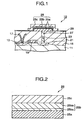
- Fig. 1 is a sectional view showing a semiconductor memory device 10 preferably manufactured by the manufacturing method in accordance with the present invention. To be more specific, Fig. 1 is a sectional view focused on a single memory cell of the semiconductor memory device 10.
- the semiconductor memory device 10 is equipped with a silicon substrate 11 serving as a semiconductor substrate, a switching device 13 and an insulating film 15 for isolating devices provided on the substrate 11, a bit line 17 and a word line 19, which partly serves as a gate electrode, that are connected to the switching device 13, an interlayer dielectric 21 in which the foregoing components 13 through 19 are buried, a contact hole 23 provided in the interlayer dielectric 21, a capacitor 25 provided on the interlayer dielectric 21, and a wire 27 in the contact hole that connects the components 13 and 25.
- Reference numeral 29 in Fig. 1 denotes a portion of a silicon nitride film formed on the interlayer dielectric at the same time when the silicon nitride film serving as a capacitor dielectric film is formed.
- the capacitor 25 is constituted by a lower electrode 25a, a capacitor dielectric film 25b composed of a silicon nitride film, and an upper electrode 25c.
- a surface of the lower electrode 25a is formed to be a roughened surface (schematically shown by circles in the drawing) in order to maximize a capacitance of the capacitor.
- the roughened surface is just an example, and dispensable.
- the lower electrode 25a itself is formed of a silicon type material, typically a doped polycrystalline silicon.
- a silicon nitride film serving as the capacitor dielectric film 25b is preferably manufactured by the method in accordance with the present invention which will be discussed hereinafter.
- the capacitor dielectric film 25b is preferably formed to include a first silicon nitride film 25ba formed by the ISN treatment and a second silicon nitride film 25bb formed by, for example, the reduced pressure CVD method in this order from the lower electrode 25a.
- the first and second silicon nitride films 25ba and 25bb are formed as the silicon nitride film 29 also on the interlayer dielectric 21.
- the semiconductor device 10 shown in Fig. 1 can be manufactured according to a procedure of the manufacturing method in accordance with the present invention described below.
- Fig. 3 and Fig. 4 show the steps of the procedure to describe the procedure.
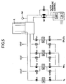
- Fig. 5 is a block diagram illustrating an example of a configuration of an apparatus for depositing a capacitor dielectric film, namely, a reduced pressure CVD apparatus or a hot wall type CVD apparatus in this case.
- Fig. 6 shows modes of carrying out and depositing conditions of embodiments and comparative examples which will be discussed hereinafter. To be more specific, Fig.
- Fig. 6 mainly shows an operating procedure and setting conditions of a main valve MV, a sub valve SV, a mechanical booster pump MBP, a diffusion pump DP, a flow rate controllers MFC 1 and 2 in the deposition apparatus shown in Fig. 5, and the degree of vacuum (a pressure at the position of a pressure gauge PM) of a deposition chamber R.
- Fig. 7 shows an example of depositing conditions when the present invention is applied, especially of a temperature profile of a specimen observed during a deposition process.
- an FET serving as a switching device and the insulating film 15 for isolating devices are formed on the semiconductor substrate 11 by a known method. Then, the bit line 17 and the word line 19 are formed by a known method.
- the switching devices 13, etc. are covered with the interlayer dielectric 21.
- the interlayer dielectric 21 a BPSG film for example, is employed.
- a contact hole 23 for exposing one source-drain region of the switching device 13 is formed in a part of the interlayer dielectric 21 by a known method.
- the wire 27 is formed in the contact hole 23 by a known method as shown in Fig. 3A.
- a doped polycrystalline silicon film (including a roughened surface polycrystalline silicon) 25x is formed as a lower electrode forming thin film on the interlayer dielectric 21 as shown in Fig. 3B.
- the formed polycrystalline silicon film is patterned according to a configuration of the lower electrode so as to produce the lower electrode 25a as shown in Fig. 3C.
- the foregoing specimen is placed in a deposition chamber (not shown).
- a temperature in the deposition chamber or a temperature of the specimen is gradually raised.
- the temperature in the deposition chamber or the temperature of the specimen is gradually increased while gradually increasing the degree of vacuum in the deposition chamber from an order of 10 -2 Pa toward 533 Pa, although this is not the only one method.
- the temperature is raised in 100°C/min. increments.
- the degree of vacuum in the deposition chamber is set at a suitable value of 533 Pa or more (e.g. 533 Pa). This condition is maintained for a predetermined period of time to perform the ISN treatment.
- the ISN treatment time is longer than a time that has been experimentally determined in advance. This will be described in more detail in conjunction with a third embodiment.
- the ISN treatment causes the lower electrode 25a to be reduced and thermally nitrided, so that even if a native oxide is produced on a surface of the lower electrode 25a, the native oxide will turn into the silicon nitride film 25ba (see Fig. 2) attributable to the ISN treatment.
- the temperature in the deposition chamber is lowered to a level suited for CVD, to a range of 650 to 700 degrees Celsius, e.g. to about 690 degrees Celsius, although it is not limited to this temperature.
- an ammonia gas and SiH 2 Cl 2 are supplied into the deposition chamber.
- a flow ratio of the ammonia gas to SiH 2 Cl 2 is set to 1:1 to 1:6, e.g. 1:5, taking dichlorosilane (SiH 2 Cl 2 ) as 1, although the ratio is not limited thereto.
- This condition is maintained for a predetermined period of time.
- the pressure in the deposition chamber at this time is set to a degree of vacuum ideally suited for deposition, ranging from 13.3 to 27 Pa, e.g.
- the silicon nitride film 25bb (see Fig. 2) from the reduced pressure CVD is formed on the silicon nitride film 25ba (see Fig. 2) from the ISN treatment. This completes the formation of the silicon nitride film 25b as the capacitor dielectric film (see Fig. 4A).
- the deposition chamber After completion of the formation of the silicon nitride film, the deposition chamber is gradually cooled, and the specimen is taken out of the deposition chamber.
- the specimen is subjected to healing oxidization.
- the healing oxidization is carried out at 850 degrees Celsius for 30 minutes in a wet oxygen atmosphere, although the condition is not limited thereto.
- a doped polycrystalline silicon film 25y for example, is formed on the specimen, which has been subjected to the healing oxidization, as shown in Fig. 4B, then the film is patterned to a configuration of the upper electrode.
- the upper electrode 25c is formed as shown in Fig. 4C.
- each memory cell is constructed by a capacitor and a transistor is completed.
- the degree of vacuum in the deposition chamber for ISN treatment is set to three different levels, namely, 160 Pa, 533 Pa, and 800 Pa, the remaining conditions such as ISN treatment time, treatment conditions, CVD deposition time, and depositing conditions being all the same.
- Semiconductor devices are fabricated at the three different degrees of vacuum according to the procedure described above. More specifically, the pressure in the deposition chamber at the time of the ISN treatment in step 5 of the depositing conditions of Fig. 6 is set to 160 Pa, 533 Pa, and 800 Pa, respectively, so as to fabricate the semiconductor devices under three different levels of vacuum.
- the film thicknesses of the silicon nitride films 25b formed on the lower electrodes 25a of the respective specimens produced under three different levels of vacuum are measured.
- the thicknesses of oxide films produced on the surfaces of the silicon nitride films 25b by healing oxidization are also measured.
- Fig. 8 The measurement results are shown in Fig. 8.
- the axis of abscissa indicates the degree of vacuum in the deposition chamber during the ISN treatment
- the left axis of ordinates indicates the film thickness of the silicon nitride film 25b formed on the lower electrode 25a
- the right axis of ordinates indicates the film thickness of an oxide film or a healing oxide film produced on the surface of the silicon nitride film 25b during the healing oxidization.
- the bar graphs provide data regarding the film thicknesses of the silicon nitride films
- the line charts provide data regarding the film thicknesses of the healing oxide films.
- the silicon nitride films of approximately the same film thicknesses namely, 5.45 nm, 5.47 nm, and 5.54 nm, are formed on the lower electrodes 25a.
- the healing oxide films at the different levels of vacuum are all thin, sharing a similar film thickness, namely, 1.30 nm, 1.28 nm, and 1.27 nm.
- the film thickness of the silicon nitride film 25b formed on the interlayer dielectric 21, and the film thickness of an oxide film produced on the surface of the silicon nitride film 25b due to the healing oxidization are measured.
- Fig. 9 The measurement results are shown in Fig. 9.
- the axis of abscissa indicates the degree of vacuum in the deposition chamber during the ISN treatment
- the left axis of ordinates indicates the film thickness of the silicon nitride film 25b formed on the interlayer dielectric 21
- the right axis of ordinates indicates the film thickness of an oxide film or a healing oxide film produced on the surface of the silicon nitride film 25b during the healing oxidization.
- the bar graphs provide data regarding the film thicknesses of the silicon nitride films
- the line charts provide data regarding the film thicknesses of the healing oxide films.
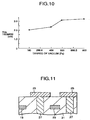
- the film thickness of the silicon nitride film formed on the interlayer dielectric was approximately 2.3 nm.
- This thickness and the foregoing film thicknesses namely, 2.0 nm, 3.1 nm, and 3.2 nm, are plotted in relation to the degree of vacuum in the deposition chamber during the ISN treatment.
- the plotting result reveals a relationship as shown in Fig. 10.
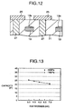
- Fig. 11 and Fig. 12 are schematic diagrams of scanning electron microscope photos showing a wiring portion of the interlayer dielectric of each device fabricated at a vacuum degree in the deposition chamber during the ISN treatment set at 533 Pa and each device fabricated at 160 Pa. Both photos are focused on a neighborhood of the word line 19. From the photo Fig. 12, it has been found that, when the degree of vacuum is set at 160 Pa, the word line or the polycrystalline silicon wire in the interlayer dielectric is also oxidized, and an abnormal oxide film 19x is produced.
- devices having capacitor dielectric films of four different film thicknesses namely, 5.0 nm, 5.5 nm, 6.0 nm, and 7.0 nm, according to the manufacturing procedure described in conjunction with the foregoing embodiment.
- a device having a capacitor dielectric of a 7.0-nm film thickness is manufactured at a degree of vacuum of 160 Pa in the deposition chamber during the ISN treatment. The capacitances of the capacitors of these five specimen devices are measured. The measurement results are shown in Fig. 13.
- the four specimen devices produced at 533 Pa provide appropriate capacitances of capacitors according to the individual film thicknesses.
- the capacitances of the capacitors of two devices manufactured with the degree of vacuum in the deposition chamber set at 160 Pa and 533 Pa for the ISN treatment are almost the same, namely, about 20 fF.
- Wire resistances ( ⁇ / ⁇ ) of the lower electrodes in the five different specimen devices manufactured in the second embodiment are measured, the measurement results being shown in Fig. 14. All the five specimen devices exhibit values of about 12.9 ⁇ / ⁇ . This means that increasing the degree of vacuum in the deposition chamber for the ISN treatment does not affect the lower electrodes.
- the manufacturing method for a semiconductor device in accordance with the present invention also provides an advantage of reducing hold time defects.
- the degree of vacuum in the deposition chamber at the time of the ISN treatment is set higher than that in the conventional method (160 Pa).
- the conventional method 160 Pa.
- more ammonia gas is contained in the ISN treatment atmosphere as compared with the conventional method, so that the volume of hydrogen generated when the ammonia gas is decomposed is likely to increase accordingly.
- an annealing effect by the hydrogen can be expected to work on the specimens.
- the film thickness of a portion of the silicon nitride film that is formed on the interlayer dielectric can be increased, making it possible to control a phenomenon of out diffusion wherein impurities contained in the interlayer dielectric diffuse out.
- specimen devices are prepared according to the procedure described in the above embodiments under four different conditions or ISN treatment times, namely, 30 minutes, 60 minutes, 90 minutes, and 120 minutes, respectively, the degree of vacuum in the deposition chamber for the ISN treatment being set at 160 Pa.
- the time spent for the CVD following the ISN treatment is set to a time required for a 5.5-nm silicon nitride film to be grown on a test silicon wafer placed in the deposition chamber.
- the film thickness of the silicon nitride film formed on the interlayer dielectric is about 3.0 nm regardless of the value of the ISN treatment time. Furthermore, it is possible to form silicon nitride films that are thicker than those produced when the ISN treatment time is shorter than 90 minutes.
- silicon nitride films are formed using the ISN treatment time as a parameter, it is meaningful, for forming a thicker silicon nitride film on the interlayer dielectric, to check beforehand a pretreatment time required for the film thickness of a portion of the silicon nitride film formed on the interlayer dielectric to reach saturation, and to set a time longer than the saturation time (90 minutes in the example shown in Fig 16) as the ISN treatment time.
- the healing oxide films of two (30-minute and 90-minute ISN treatment times) out of the four specimen devices will now be discussed. More specifically, regarding these two specimen devices, the thicknesses of the healing oxide films produced in the silicon nitride film portions on the lower electrodes after the silicon nitride films have been subjected to healing oxidization are measured.
- Fig. 17 and Fig. 18 The measurement results are shown in Fig. 17 and Fig. 18. Wherein the thicknesses of silicon nitride films are also shown.
- Fig. 17 provides data regarding the thicknesses of silicon nitride films on the lower electrodes and the thicknesses of healing oxide films
- Fig. 18 provides data regarding the thicknesses of silicon nitride films on the interlayer dielectrics and the thicknesses of healing oxide films.
- the axis of abscissa indicates the ISN treatment time
- the left axis of ordinates indicates the thickness of the silicon nitride film
- the right axis of ordinates indicates the thickness of the healing oxide film.
- the bar graphs provide data regarding the film thicknesses of the silicon nitride films
- the line charts provide data regarding the film thicknesses of the healing oxide films.
- the values of the thicknesses of the healing oxide films on the lower electrodes are nearly the same irrespective of the ISN treatment time.
- the thickness of the healing oxide film produced when the ISN treatment time is 30 minutes is 56 nm, while the thickness is approximately 1.0 nm, which is only 1/56 of the former, meaning improved resistance to oxidization, when the ISN treatment time is 90 minutes.
- the ISN treatment time should be set to a predetermined time (90 minutes in the example of Fig. 16) or longer.
- a semiconductor device to which the manufacturing method of the present invention is applicable is by no means limited to the device discussed in conjunction with Fig. 1.
- the manufacturing method of the invention can be extensively applied to the manufacture of semiconductor devices provided with capacitors on interlayer dielectrics, the capacitors employing silicon nitride films as capacitor dielectric films.
- SiH 2 Cl 2 has been used, together with the ammonia gas, as the gas for forming a silicon type thin film.
- the gas for forming the silicon type thin film is not limited thereto; other suitable gases may be used instead.
- the reduced pressure, hot wall type CVD apparatus has been used as the apparatus for implementing the ISN treatment and the apparatus for forming the silicon nitride films.
- the apparatus is not limited thereto, and a nitriding furnace having the same structure as that of a high-pressure oxidizing furnace or a cold wall type rapid thermal processing (RTP) apparatus or rapid thermal nitride apparatus may be used to obtain the same advantages as those effected by the foregoing embodiments.
- RTP rapid thermal processing
- the manufacturing method for a semiconductor device in accordance with the present invention includes the steps of: forming a lower electrode composed of a silicon type material on an interlayer dielectric, placing a specimen on which the lower electrode has been formed in a deposition chamber to perform pretreatment in which heat is applied to the specimen in the deposition chamber wherein pressure has been reduced an ammonia gas atmosphere has been set, then introducing an ammonia gas and a gas for forming a silicon type thin film into the deposition chamber to form a silicon nitride film on the lower electrode and the interlayer dielectric, wherein a degree of vacuum in the deposition chamber at the time of the pretreatment is set to 533 Pa or more, and a time for the pretreatment is set to be longer than the aforesaid saturation time.
- the a portion of the silicon nitride film that is formed on the interlayer dielectric can be made thicker, so that the oxidization resistance of the silicon nitride film on the interlayer dielectric is improved. This makes it possible to prevent abnormal oxidization of wires under interlayer dielectrics at the time of healing oxidization after silicon nitride films are formed.
Landscapes
- Engineering & Computer Science (AREA)
- Manufacturing & Machinery (AREA)
- Semiconductor Memories (AREA)
- Semiconductor Integrated Circuits (AREA)
- Formation Of Insulating Films (AREA)
Abstract
Description
Claims (8)
- A manufacturing method for a semiconductor device that has a capacitor electrode having a silicon nitride film as a capacitor dielectric film, comprising the steps of:forming a lower electrode on an interlayer dielectric; andcarrying out reduction and thermal nitriding on a specimen, on which said lower electrode has been formed, in an ammonia gas atmosphere in a deposition chamber wherein pressure has been reduced to a range from 533 Pa to 1333 Pa, then forming a silicon nitride film on said lower electrode and said interlayer dielectric.
- The method according to claim 1, wherein a time for carrying out said reduction and thermal nitriding is longer than a film thickness saturation time of said silicon nitride film formed on said interlayer dielectric.
- A manufacturing method for a semiconductor device that has a capacitor electrode having a silicon nitride film as a capacitor dielectric film, comprising the steps of:forming a lower electrode on an interlayer dielectric; andcarrying out reduction and thermal nitriding on a specimen, on which said lower electrode has been formed, in an ammonia gas atmosphere in a deposition chamber wherein pressure has been reduced, then forming a silicon nitride film on said lower electrode and said interlayer dielectric,
wherein a time for carrying out said reduction and thermal nitriding is longer than a film thickness saturation time of said silicon nitride film formed on said interlayer dielectric. - The method according to any of the claims 1 to 3, further comprising a step of subjecting the specimen, on which said silicon nitride film has been formed, to heat treatment.
- The method according to any of the claims 1 to 3, wherein said lower electrode is formed of a silicon type material.
- The method according to claim 5, wherein polycrystalline silicon is employed as a silicon type material composing said lower electrode.
- The method according to any of the claims 1 to 3, wherein an ammonia gas and a gas for forming a silicon type thin film are used for forming said silicon nitride film.
- The method according to claim 7, wherein dichlorosilane (SiH2Cl2) is used as said gas for forming a silicon type thin film.
Applications Claiming Priority (2)
| Application Number | Priority Date | Filing Date | Title |
|---|---|---|---|
| JP11364399 | 1999-04-21 | ||
| JP11364399A JP3350478B2 (en) | 1999-04-21 | 1999-04-21 | Method for manufacturing semiconductor device |
Publications (2)
| Publication Number | Publication Date |
|---|---|
| EP1047117A2 true EP1047117A2 (en) | 2000-10-25 |
| EP1047117A3 EP1047117A3 (en) | 2003-01-29 |
Family
ID=14617452
Family Applications (1)
| Application Number | Title | Priority Date | Filing Date |
|---|---|---|---|
| EP00104967A Withdrawn EP1047117A3 (en) | 1999-04-21 | 2000-03-08 | Method for manufacturing a silicon nitride capacitor dielectric film |
Country Status (5)
| Country | Link |
|---|---|
| US (1) | US6319763B1 (en) |
| EP (1) | EP1047117A3 (en) |
| JP (1) | JP3350478B2 (en) |
| KR (1) | KR100697773B1 (en) |
| TW (1) | TW469498B (en) |
Cited By (3)
| Publication number | Priority date | Publication date | Assignee | Title |
|---|---|---|---|---|
| EP1312697A1 (en) * | 2001-11-16 | 2003-05-21 | ASML US, Inc. | CVD of dielectric films |
| WO2003028069A3 (en) * | 2001-09-25 | 2003-12-11 | Applied Materials Inc | Method for cyclic cvd |
| CN110678959A (en) * | 2017-05-25 | 2020-01-10 | 应用材料公司 | High pressure processing of silicon nitride films |
Families Citing this family (4)
| Publication number | Priority date | Publication date | Assignee | Title |
|---|---|---|---|---|
| KR100866451B1 (en) * | 2002-06-12 | 2008-10-31 | 동부일렉트로닉스 주식회사 | Certification body for calibration of semiconductor defect inspection equipment and its manufacturing method |
| US20070080426A1 (en) * | 2005-10-11 | 2007-04-12 | Texas Instruments Incorporated | Single lithography-step planar metal-insulator-metal capacitor and resistor |
| USD1084879S1 (en) * | 2023-06-28 | 2025-07-22 | Hollister Incorporated | Packaging for sensing accessory |
| USD1084880S1 (en) * | 2023-06-28 | 2025-07-22 | Hollister Incorporated | Packaging for sensing accessory |
Family Cites Families (12)
| Publication number | Priority date | Publication date | Assignee | Title |
|---|---|---|---|---|
| DE2967704D1 (en) * | 1978-06-14 | 1991-06-13 | Fujitsu Ltd | METHOD FOR PRODUCING A SEMICONDUCTOR ARRANGEMENT WITH AN INSULATION LAYER. |
| US4623912A (en) * | 1984-12-05 | 1986-11-18 | At&T Bell Laboratories | Nitrided silicon dioxide layers for semiconductor integrated circuits |
| US5290729A (en) * | 1990-02-16 | 1994-03-01 | Mitsubishi Denki Kabushiki Kaisha | Stacked type capacitor having a dielectric film formed on a rough surface of an electrode and method of manufacturing thereof |
| JPH0567751A (en) * | 1991-09-09 | 1993-03-19 | Miyazaki Oki Electric Co Ltd | Semiconductor device and manufacture thereof |
| US5250456A (en) * | 1991-09-13 | 1993-10-05 | Sgs-Thomson Microelectronics, Inc. | Method of forming an integrated circuit capacitor dielectric and a capacitor formed thereby |
| JPH05109981A (en) * | 1991-10-21 | 1993-04-30 | Nec Corp | Manufacture of semiconductor device |
| US5397748A (en) * | 1991-12-28 | 1995-03-14 | Nec Corporation | Method of producing semiconductor device with insulating film having at least silicon nitride film |
| US5478765A (en) * | 1994-05-04 | 1995-12-26 | Regents Of The University Of Texas System | Method of making an ultra thin dielectric for electronic devices |
| JP3660391B2 (en) * | 1994-05-27 | 2005-06-15 | 株式会社東芝 | Manufacturing method of semiconductor device |
| JPH08167605A (en) * | 1994-12-15 | 1996-06-25 | Mitsubishi Electric Corp | Method of manufacturing silicon nitride film |
| JPH0950996A (en) * | 1995-08-07 | 1997-02-18 | Ulvac Japan Ltd | Method for forming silicon nitride film and silicon nitride film |
| JPH118359A (en) * | 1997-06-17 | 1999-01-12 | Oki Electric Ind Co Ltd | Capacitor insulating film and method of manufacturing the same |
-
1999
- 1999-04-21 JP JP11364399A patent/JP3350478B2/en not_active Expired - Fee Related
-
2000
- 2000-02-04 US US09/497,500 patent/US6319763B1/en not_active Expired - Fee Related
- 2000-03-08 EP EP00104967A patent/EP1047117A3/en not_active Withdrawn
- 2000-03-09 KR KR1020000011750A patent/KR100697773B1/en not_active Expired - Fee Related
- 2000-03-14 TW TW089104573A patent/TW469498B/en not_active IP Right Cessation
Cited By (4)
| Publication number | Priority date | Publication date | Assignee | Title |
|---|---|---|---|---|
| WO2003028069A3 (en) * | 2001-09-25 | 2003-12-11 | Applied Materials Inc | Method for cyclic cvd |
| EP1312697A1 (en) * | 2001-11-16 | 2003-05-21 | ASML US, Inc. | CVD of dielectric films |
| CN110678959A (en) * | 2017-05-25 | 2020-01-10 | 应用材料公司 | High pressure processing of silicon nitride films |
| CN110678959B (en) * | 2017-05-25 | 2023-07-25 | 应用材料公司 | High Pressure Processing of Silicon Nitride Film |
Also Published As
| Publication number | Publication date |
|---|---|
| JP3350478B2 (en) | 2002-11-25 |
| KR100697773B1 (en) | 2007-03-21 |
| US6319763B1 (en) | 2001-11-20 |
| JP2000307082A (en) | 2000-11-02 |
| EP1047117A3 (en) | 2003-01-29 |
| KR20000076799A (en) | 2000-12-26 |
| TW469498B (en) | 2001-12-21 |
Similar Documents
| Publication | Publication Date | Title |
|---|---|---|
| US6472319B2 (en) | Method for manufacturing capacitor of semiconductor memory device by two-step thermal treatment | |
| US20050020018A1 (en) | Method of manufacturing a semiconductor integrated circuit device | |
| US6784100B2 (en) | Capacitor with oxidation barrier layer and method for manufacturing the same | |
| JP2000200889A (en) | Method for manufacturing capacitor having tantalum oxide film | |
| JPH1074898A (en) | Method for manufacturing capacitor of semiconductor device | |
| US6800519B2 (en) | Semiconductor device and method of manufacturing the same | |
| US7064052B2 (en) | Method of processing a transistor gate dielectric film with stem | |
| US6319763B1 (en) | Manufacturing method for semiconductor device | |
| US6228701B1 (en) | Apparatus and method for minimizing diffusion in stacked capacitors formed on silicon plugs | |
| JP2002353214A (en) | Method for manufacturing semiconductor device | |
| JPH1022455A (en) | Semiconductor device and manufacturing method thereof | |
| JP2006135229A (en) | Method for forming insulating film and semiconductor device provided with the insulating film | |
| JPH09115904A (en) | Method for producing oxide film and apparatus for producing oxide film | |
| KR20010085446A (en) | Manufacturing method of semiconductor device having tantalum oxide film | |
| KR100190025B1 (en) | Capacitor fabrication method of semiconductor device | |
| KR100347400B1 (en) | A method for manufacturing a semiconductor device | |
| JP5039396B2 (en) | Manufacturing method of semiconductor device | |
| US7763500B2 (en) | Method for manufacturing semiconductor storage device comprising a slow cooling step | |
| JP3552846B2 (en) | Semiconductor device and manufacturing method thereof | |
| KR100231604B1 (en) | Manufacturing method of capacitor of semiconductor device | |
| JP3216122B2 (en) | Method of forming capacitive element | |
| GB2347787A (en) | Method of forming a tantalum oxide containing capacitor | |
| KR100721203B1 (en) | Semiconductor device having ternary oxide gate insulating film and method of manufacturing the same | |
| JP2000323679A (en) | Semiconductor device and manufacturing method thereof | |
| JPH05175423A (en) | Manufacture of semiconductor device |
Legal Events
| Date | Code | Title | Description |
|---|---|---|---|
| PUAI | Public reference made under article 153(3) epc to a published international application that has entered the european phase |
Free format text: ORIGINAL CODE: 0009012 |
|
| AK | Designated contracting states |
Kind code of ref document: A2 Designated state(s): AT BE CH CY DE DK ES FI FR GB GR IE IT LI LU MC NL PT SE |
|
| AX | Request for extension of the european patent |
Free format text: AL;LT;LV;MK;RO;SI |
|
| PUAL | Search report despatched |
Free format text: ORIGINAL CODE: 0009013 |
|
| AK | Designated contracting states |
Designated state(s): AT BE CH CY DE DK ES FI FR GB GR IE IT LI LU MC NL PT SE |
|
| AX | Request for extension of the european patent |
Extension state: AL LT LV MK RO SI |
|
| RIC1 | Information provided on ipc code assigned before grant |
Ipc: 7H 01L 21/321 B Ipc: 7H 01L 21/8242 B Ipc: 7H 01L 27/108 B Ipc: 7H 01L 21/314 B Ipc: 7H 01L 21/02 B Ipc: 7H 01L 21/318 A |
|
| 17P | Request for examination filed |
Effective date: 20030728 |
|
| AKX | Designation fees paid |
Designated state(s): DE FR GB NL |
|
| 17Q | First examination report despatched |
Effective date: 20050301 |
|
| STAA | Information on the status of an ep patent application or granted ep patent |
Free format text: STATUS: THE APPLICATION IS DEEMED TO BE WITHDRAWN |
|
| 18D | Application deemed to be withdrawn |
Effective date: 20101001 |