EP1042801B1 - Selektive herstellung von silizidschichten - Google Patents
Selektive herstellung von silizidschichten Download PDFInfo
- Publication number
- EP1042801B1 EP1042801B1 EP99941507A EP99941507A EP1042801B1 EP 1042801 B1 EP1042801 B1 EP 1042801B1 EP 99941507 A EP99941507 A EP 99941507A EP 99941507 A EP99941507 A EP 99941507A EP 1042801 B1 EP1042801 B1 EP 1042801B1
- Authority
- EP
- European Patent Office
- Prior art keywords
- layer
- silicon
- applying
- silicide
- mask
- Prior art date
- Legal status (The legal status is an assumption and is not a legal conclusion. Google has not performed a legal analysis and makes no representation as to the accuracy of the status listed.)
- Expired - Lifetime
Links
Images


Classifications
-
- H—ELECTRICITY
- H10—SEMICONDUCTOR DEVICES; ELECTRIC SOLID-STATE DEVICES NOT OTHERWISE PROVIDED FOR
- H10D—INORGANIC ELECTRIC SEMICONDUCTOR DEVICES
- H10D64/00—Electrodes of devices having potential barriers
- H10D64/01—Manufacture or treatment
- H10D64/011—Manufacture or treatment of electrodes ohmically coupled to a semiconductor
- H10D64/0111—Manufacture or treatment of electrodes ohmically coupled to a semiconductor to Group IV semiconductors
- H10D64/0112—Manufacture or treatment of electrodes ohmically coupled to a semiconductor to Group IV semiconductors using conductive layers comprising silicides
-
- H—ELECTRICITY
- H10—SEMICONDUCTOR DEVICES; ELECTRIC SOLID-STATE DEVICES NOT OTHERWISE PROVIDED FOR
- H10D—INORGANIC ELECTRIC SEMICONDUCTOR DEVICES
- H10D84/00—Integrated devices formed in or on semiconductor substrates that comprise only semiconducting layers, e.g. on Si wafers or on GaAs-on-Si wafers
- H10D84/01—Manufacture or treatment
- H10D84/0123—Integrating together multiple components covered by H10D12/00 or H10D30/00, e.g. integrating multiple IGBTs
- H10D84/0126—Integrating together multiple components covered by H10D12/00 or H10D30/00, e.g. integrating multiple IGBTs the components including insulated gates, e.g. IGFETs
- H10D84/0135—Manufacturing their gate conductors
- H10D84/0137—Manufacturing their gate conductors the gate conductors being silicided
-
- H—ELECTRICITY
- H10—SEMICONDUCTOR DEVICES; ELECTRIC SOLID-STATE DEVICES NOT OTHERWISE PROVIDED FOR
- H10D—INORGANIC ELECTRIC SEMICONDUCTOR DEVICES
- H10D84/00—Integrated devices formed in or on semiconductor substrates that comprise only semiconducting layers, e.g. on Si wafers or on GaAs-on-Si wafers
- H10D84/01—Manufacture or treatment
- H10D84/02—Manufacture or treatment characterised by using material-based technologies
- H10D84/03—Manufacture or treatment characterised by using material-based technologies using Group IV technology, e.g. silicon technology or silicon-carbide [SiC] technology
- H10D84/038—Manufacture or treatment characterised by using material-based technologies using Group IV technology, e.g. silicon technology or silicon-carbide [SiC] technology using silicon technology, e.g. SiGe
-
- H—ELECTRICITY
- H10—SEMICONDUCTOR DEVICES; ELECTRIC SOLID-STATE DEVICES NOT OTHERWISE PROVIDED FOR
- H10W—GENERIC PACKAGES, INTERCONNECTIONS, CONNECTORS OR OTHER CONSTRUCTIONAL DETAILS OF DEVICES COVERED BY CLASS H10
- H10W10/00—Isolation regions in semiconductor bodies between components of integrated devices
- H10W10/01—Manufacture or treatment
- H10W10/011—Manufacture or treatment of isolation regions comprising dielectric materials
- H10W10/014—Manufacture or treatment of isolation regions comprising dielectric materials using trench refilling with dielectric materials, e.g. shallow trench isolations
-
- H—ELECTRICITY
- H10—SEMICONDUCTOR DEVICES; ELECTRIC SOLID-STATE DEVICES NOT OTHERWISE PROVIDED FOR
- H10W—GENERIC PACKAGES, INTERCONNECTIONS, CONNECTORS OR OTHER CONSTRUCTIONAL DETAILS OF DEVICES COVERED BY CLASS H10
- H10W10/00—Isolation regions in semiconductor bodies between components of integrated devices
- H10W10/10—Isolation regions comprising dielectric materials
- H10W10/17—Isolation regions comprising dielectric materials formed using trench refilling with dielectric materials, e.g. shallow trench isolations
-
- H—ELECTRICITY
- H10—SEMICONDUCTOR DEVICES; ELECTRIC SOLID-STATE DEVICES NOT OTHERWISE PROVIDED FOR
- H10W—GENERIC PACKAGES, INTERCONNECTIONS, CONNECTORS OR OTHER CONSTRUCTIONAL DETAILS OF DEVICES COVERED BY CLASS H10
- H10W20/00—Interconnections in chips, wafers or substrates
- H10W20/01—Manufacture or treatment
- H10W20/031—Manufacture or treatment of conductive parts of the interconnections
- H10W20/064—Manufacture or treatment of conductive parts of the interconnections by modifying the conductivity of conductive parts, e.g. by alloying
- H10W20/066—Manufacture or treatment of conductive parts of the interconnections by modifying the conductivity of conductive parts, e.g. by alloying by forming silicides of refractory metals
Definitions
- the invention relates to a method of selectively forming silicide comprising the steps of:
- Such methods are known from JP-A-07161949.
- a semiconductor body with exposed silicon regions is covered with an oxide film.
- a patterned resist layer is applied and the oxide film is locally removed.
- a high melting point metal is applied and silicide is formed at the location where the oxide film was locally removed.
- US-5,589,423 discloses a method of selectively forming a silicide wherein a gate oxide layer overlies a substrate surface.
- a silicide blocking layer is formed over the substrate which is then partially etched through an etching mask. The etching mask is removed and the etch is resumed. The exposed portions of the gate oxide layer are removed before silicidation takes place.
- the method according to the invention is defined in claim 1 and is characterized in that the mask layer is formed by:
- the second etch process can be controlled more accurately so that the definition of the mask layer is improved.
- the second layer can be etched selectively relative to the first layer by means of commonly used techniques so that the first layer can be relatively thin and hence easily patterned with a good definition.
- the silicon is protected by the silicon oxide top layer during deposition and etching of the first layer. Due to this protection, contamination of the silicon is further counteracted. If the top layer has a thickness of less than 20nm, this top layer will not prevent the formation of silicide. However, it is preferred to remove the top layer before depositing the material capable of silicide-formation. This can, for example, be achieved by immersion in HF.
- the spacers are also etched during etching of the first layer. Consequently, a larger part of the side portions of the silicon ridges come into contact with the material capable of silicide-formation so that the silicide formation is improved and the resistance of the ridges is decreased.
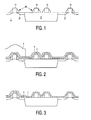
- Fig. 1 shows a detail of a crystalline silicon body 1 wherein a shallow trench insulation 2 is made by etching a groove and filling it with silicon oxide. Ridges 11, 12, 13 and 14 of polysilicon are made on the surface of the silicon body 1 by applying a layer of polysilicon and patterning it with a known technique. Spacers 20 of silicon nitride are provided on the side walls of the polysilicon ridges 11, 12, 13 and 14. In a subsequent diffusion process, these spacers function as filters in order to obtain proper diffusion profiles 21.
- a silicon oxide top layer (not shown) with a thickness of 3 nm is formed on the silicon by oxidizing the silicon.
- Fig. 2 shows the detail of Fig. 1 after applying a first layer 3 of silicon nitride, a second layer 5 of TEOS and a patterned resist layer 7.
- the silicon nitride layer 3 has a thickness of 30 nm and has been applied by LPCVD at 780 °C.
- the TEOS layer 5 has a thickness of 42 nm and has been applied by PECVD at 450 °C.
- Fig. 3 shows the same detail after etching the second layer 5 and stripping the resist layer 7.
- the TEOS layer 5 has been etched by immersion in a solution of 0.36% HF during 14 minutes. Subsequently, the resist has been stripped in H 2 SO 4 or peroxide.
- Fig. 4 shows the detail of the semiconductor body 1 after etching the first layer 3.
- the silicon nitride layer 3 has been etched by immersion in H 3 PO 4 of 165 °C during 15 minutes using the TEOS layer 5 as a mask. Due to this etch step, the spacers are partly etched so that a larger part of the ridges comes into contact with the titanium.
- Fig. 5 shows the same detail after applying a titanium layer, forming silicide by means of a thermal treatment and removing the titanium which has not reacted to form titanium silicide.
- the titanium layer has a thickness of 30 nm and has been deposited by PVD.
- the silicon oxide top layer if present, is removed by dipping the body 1 in an HF solution. Subsequently, the body is rapidly heated to a temperature of 760 °C at which it is kept for 20 seconds.
- titanium silicide 21, 22 is formed at locations where the titanium was in contact with silicon regions i.e. on top of the polysilicon ridges 12, 13 and 14 and also on the exposed crystalline silicon regions 23 and 24.
- titanium not in contact with silicon regions has reacted with the material of the spacers and the isolating material so that titanium nitride and titanium oxide is formed.
- This titanium nitride and titanium oxide is removed with an etchant containing ammonia and peroxide which etchant is selective relative to titanium silicide.
- the body is rapidly heated to 850 °C at which temperature it is kept for 20 seconds in order to transform the titanium silicide to its low resistivity C54 phase.
- Fig. 6 shows the sheet resistance of silicidized 0.25 micrometer wide p+ polysilicon lines of samples made by means of the method according to the invention in comparison to that of samples made by a prior art method. On the vertical scale the sheet resistance is expressed in Ohm per Square.
- the box-plots 61. 62 and 63, respectively, correspond to three different batches of forty five samples which where etched in phosphoric acid for 11 minutes, 14 minutes and 16 minutes, respectively.
- the box-plot 64 corresponds to a batch of thirty six samples made by a method wherein the mask layer is formed by applying a 68 nm thick TEOS layer and partial removal of the TEOS layer by plasma etching.
- Each box-plot is dimensioned as follows: the large horizontal line in the box corresponds to the median of the measurement values; the bounding lines of the box indicate the limit of 50% of the measurement values around the median; the small horizontal lines indicate the highest and lowest measurement values, values lying beyond said measurement values being excluded.
- Fig. 7 shows the sheet resistance of silicidized N+ diffused crystalline silicon regions of samples made by means of the method according to the invention in comparison to that of samples made by the prior art method. On the vertical scale the sheet resistance is expressed in Ohm per square.
- the box-plots 71, 72 and 73, respectively, correspond to three different batches of forty five samples which where etched in phosphoric acid for 11 minutes, 14 minutes and 16 minutes, respectively.
- the box-plot 74 corresponds to a batch of thirty six samples made by a method wherein the mask layer is formed by applying a 68 nm thick TEOS layer and partial removal of the TEOS layer by plasma etching.
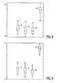
- Fig. 8 shows the contact resistance on silicidized N+ diffused polysilicon regions of samples made by means of the method according to the invention in comparison to that of samples made by the prior art method.
- the contact resistance is expressed in Ohm per contact.
- the contact resistance is measured with a so-called Kelvin structure consisting of many tungsten contacts.
- the box-plots 81, 82 and 83, respectively, correspond to three different batches of forty five samples which where etched in phosphoric acid for 11 minutes, 14 minutes and 16 minutes, respectively.
- the box-plot 84 corresponds to a batch of thirty six samples made by a method wherein the mask layer is formed by applying a 68 nm thick TEOS layer and partial removal of the TEOS layer by plasma etching.
- Fig. 9 shows the contact resistance on silicidized N+ diffused crystalline silicon regions of samples made by means of the method according to the invention in comparison to that of samples made by a prior art method.
- the contact resistance is expressed in Ohm per contact.
- the box-plots 91, 92 and 93, respectively, correspond to three different batches of forty five samples which where etched in phosphoric acid for 11 minutes, 14 minutes and 16 minutes, respectively.
- the box-plot 94 corresponds to a batch of thirty six samples made by a method wherein the mask layer is formed by applying a 68 nm thick TEOS layer and partial removal of the TEOS layer by plasma etching.
- the invention is not limited to the embodiments described above.
- the material capable of silicide-formation may for example also be Ni, W, Co, Fe, Mo or Pt.
- the first and the second material are also possible.
- the first material may be a silicon nitride or silicon oxynitride formed by any means
- the second material may be a silicon oxide formed by any means
- the first etch process may be either a wet process or a plasma process
- the second etchant may be any wet oxynitride-etchant or wet nitride-etchant which is selective relative to the silicon regions or, if a silicon oxide top layer is used, a plasma oxynitride-etchant or plasma nitride-etchant which is selective relative to the silicon oxide top layer.
Landscapes
- Electrodes Of Semiconductors (AREA)
- Internal Circuitry In Semiconductor Integrated Circuit Devices (AREA)
- Weting (AREA)
- Metal-Oxide And Bipolar Metal-Oxide Semiconductor Integrated Circuits (AREA)
- Insulated Gate Type Field-Effect Transistor (AREA)
Claims (7)
- Verfahren zum selektiven Bilden von Silizid, mit den Schritten:- Vorsehen eines Körpers mit Silizium-Regionen,- Anbringen einer Maskenschicht, welche einen Teil der Silizium-Regionen abdeckt,- Anbringen eines passenden Materials, welches zur Silizid-Formation in der Lage ist, und- Bilden von Silizid durch Induzieren einer Reaktion zwischen dem Material und Silizium von nicht abgedeckten Silizium-Regionen, dadurch gekennzeichnet, dass die Maskenschicht gebildet wird durch- Anbringen einer ersten Schicht aus Siliziumnitrid;- Anbringen einer zweiten Schicht aus Siliziumoxid;- Anbringen einer strukturierten Lackschicht,- Ätzen der zweiten Schicht mittels eines ersten Ätzprozesses unter Verwendung der strukturierten Lackschicht als eine Maske, und- Ätzen der ersten Schicht unter Verwendung der zweiten Schicht als eine Maske mittels eines zweiten Ätzprozesses, der bezüglich der Silizium-Regionen hoch selektiv ist.
- Verfahren nach Anspruch 1, dadurch gekennzeichnet, dass die Lackschicht vor einem Ätzen der ersten Schicht entfernt wird.
- Verfahren nach Anspruch 2, dadurch gekennzeichnet, dass der zweite Ätzprozess ein Nassätzprozess unter Verwendung von Phosphorsäure ist.
- Verfahren nach Anspruch 1, dadurch gekennzeichnet, dass das Verfahren weiterhin einen Schritt eines Vorsehens der Silizium-Regionen mit einer oberen Siliziumoxidschicht vor einem Anbringen der Maskenschicht aufweist.
- Verfahren nach Anspruch 4, dadurch gekennzeichnet, dass das Verfahren weiterhin einen Schritt eines Entfernens der oberen Siliziumoxidschicht vor einem Anbringen des Materials, welches zur Silizid-Formation in der Lage ist, aufweist.
- Verfahren nach Anspruch 1, dadurch gekennzeichnet, dass das Verfahren weiterhin, vor dem Schritt eines Anbringens der Maskenschicht, den Schritt eines Vorsehens von Silizium-Erhöhungen auf dem Körper aufweist, wobei die Erhöhungen einen oberen exponierten Abschnitt und sich von dem oberen Abschnitt zu einem Bodenabschnitt erstreckende exponierte Seitenabschnitte aufweisen, und wobei der erste und der zweite Ätzprozess isotrope Ätzprozesse sind.
- Verfahren nach Anspruch 6, dadurch gekennzeichnet, dass das Verfahren weiterhin einen Schritt eines Bildens von Siliziumnitrid-Spacern auf den Seitenabschnitten in der Nähe des Bodenabschnittes aufweist.
Priority Applications (1)
| Application Number | Priority Date | Filing Date | Title |
|---|---|---|---|
| EP99941507A EP1042801B1 (de) | 1998-08-11 | 1999-08-02 | Selektive herstellung von silizidschichten |
Applications Claiming Priority (4)
| Application Number | Priority Date | Filing Date | Title |
|---|---|---|---|
| EP98402032 | 1998-08-11 | ||
| EP98402032 | 1998-08-11 | ||
| EP99941507A EP1042801B1 (de) | 1998-08-11 | 1999-08-02 | Selektive herstellung von silizidschichten |
| PCT/EP1999/005589 WO2000010198A1 (en) | 1998-08-11 | 1999-08-02 | Method of selectively forming silicide |
Publications (2)
| Publication Number | Publication Date |
|---|---|
| EP1042801A1 EP1042801A1 (de) | 2000-10-11 |
| EP1042801B1 true EP1042801B1 (de) | 2007-05-02 |
Family
ID=8235469
Family Applications (1)
| Application Number | Title | Priority Date | Filing Date |
|---|---|---|---|
| EP99941507A Expired - Lifetime EP1042801B1 (de) | 1998-08-11 | 1999-08-02 | Selektive herstellung von silizidschichten |
Country Status (5)
| Country | Link |
|---|---|
| US (1) | US6677234B1 (de) |
| EP (1) | EP1042801B1 (de) |
| JP (1) | JP2002522921A (de) |
| DE (1) | DE69935965T2 (de) |
| WO (1) | WO2000010198A1 (de) |
Families Citing this family (2)
| Publication number | Priority date | Publication date | Assignee | Title |
|---|---|---|---|---|
| US7132365B2 (en) * | 2004-08-10 | 2006-11-07 | Texas Instruments Incorporated | Treatment of silicon prior to nickel silicide formation |
| US20080237811A1 (en) * | 2007-03-30 | 2008-10-02 | Rohit Pal | Method for preserving processing history on a wafer |
Family Cites Families (9)
| Publication number | Priority date | Publication date | Assignee | Title |
|---|---|---|---|---|
| KR910006249B1 (ko) * | 1983-04-01 | 1991-08-17 | 가부시기가이샤 히다찌세이사꾸쇼 | 반도체 장치 |
| US4931411A (en) * | 1985-05-01 | 1990-06-05 | Texas Instruments Incorporated | Integrated circuit process with TiN-gate transistor |
| JPH07161949A (ja) | 1993-12-02 | 1995-06-23 | Hitachi Ltd | 固体撮像装置とその製造方法 |
| US5589423A (en) * | 1994-10-03 | 1996-12-31 | Motorola Inc. | Process for fabricating a non-silicided region in an integrated circuit |
| US5956610A (en) * | 1997-05-22 | 1999-09-21 | Advanced Micro Devices, Inc. | Method and system for providing electrical insulation for local interconnect in a logic circuit |
| US5933739A (en) * | 1997-09-11 | 1999-08-03 | Vlsi Technology, Inc. | Self-aligned silicidation structure and method of formation thereof |
| US5924011A (en) * | 1997-12-15 | 1999-07-13 | Taiwan Semiconductor Manufacturing Company, Ltd. | Silicide process for mixed mode product |
| US5872063A (en) * | 1998-01-12 | 1999-02-16 | Taiwan Semiconductor Manufacturing Company Ltd. | Self-aligned contact structures using high selectivity etching |
| US6004878A (en) * | 1998-02-12 | 1999-12-21 | National Semiconductor Corporation | Method for silicide stringer removal in the fabrication of semiconductor integrated circuits |
-
1999
- 1999-08-02 DE DE69935965T patent/DE69935965T2/de not_active Expired - Lifetime
- 1999-08-02 WO PCT/EP1999/005589 patent/WO2000010198A1/en not_active Ceased
- 1999-08-02 JP JP2000565563A patent/JP2002522921A/ja active Pending
- 1999-08-02 EP EP99941507A patent/EP1042801B1/de not_active Expired - Lifetime
- 1999-08-06 US US09/369,539 patent/US6677234B1/en not_active Expired - Fee Related
Non-Patent Citations (1)
| Title |
|---|
| None * |
Also Published As
| Publication number | Publication date |
|---|---|
| JP2002522921A (ja) | 2002-07-23 |
| EP1042801A1 (de) | 2000-10-11 |
| DE69935965D1 (de) | 2007-06-14 |
| US6677234B1 (en) | 2004-01-13 |
| DE69935965T2 (de) | 2008-01-10 |
| WO2000010198A1 (en) | 2000-02-24 |
Similar Documents
| Publication | Publication Date | Title |
|---|---|---|
| EP0128304B1 (de) | Verfahren zum Herstellen eines metallischen Silizids | |
| US4877755A (en) | Method of forming silicides having different thicknesses | |
| US5783475A (en) | Method of forming a spacer | |
| EP0562127A1 (de) | Verfahren zur Herstellung einer Halbleiteranordnung | |
| US6475893B2 (en) | Method for improved fabrication of salicide structures | |
| US5605865A (en) | Method for forming self-aligned silicide in a semiconductor device using vapor phase reaction | |
| US7119024B2 (en) | Method and structure for a self-aligned silicided word line and polysilicon plug during the formation of a semiconductor device | |
| US5326724A (en) | Oxide-capped titanium silicide formation | |
| US6677234B1 (en) | Method of selectively forming silicide | |
| KR100291513B1 (ko) | 반도체 소자의 제조방법 | |
| US6847085B2 (en) | High aspect ratio contact surfaces having reduced contaminants | |
| EP0392725B1 (de) | Verfahren zum Herstellen von integrierten Schaltungen mit Silizid | |
| KR100847365B1 (ko) | 잔류물 제거시 보조하기 위한 등방성 저항기 보호 식각 | |
| US6255173B1 (en) | Method of forming gate electrode with titanium polycide structure | |
| JPH08306783A (ja) | 半導体装置のコンタクト形成方法 | |
| KR0147868B1 (ko) | 반도체 소자 격리방법 | |
| US6046113A (en) | Combined dry and wet etch for improved silicide formation | |
| US6037254A (en) | Method of making a surface protective layer for improved silicide formation | |
| US6114733A (en) | Surface protective layer for improved silicide formation | |
| JP3435943B2 (ja) | 半導体装置およびその製造方法 | |
| KR100548598B1 (ko) | 반도체소자의 캐패시터 제조방법 | |
| JPS6279625A (ja) | 半導体装置の製造方法 | |
| KR19980065709A (ko) | 샐리사이드 제조방법 | |
| KR100266002B1 (ko) | 반도체장치의 제조방법 | |
| KR100390817B1 (ko) | 반도체소자 제조방법 |
Legal Events
| Date | Code | Title | Description |
|---|---|---|---|
| PUAI | Public reference made under article 153(3) epc to a published international application that has entered the european phase |
Free format text: ORIGINAL CODE: 0009012 |
|
| AK | Designated contracting states |
Kind code of ref document: A1 Designated state(s): AT BE CH CY DE DK ES FI FR GB GR IE IT LI LU MC NL PT SE |
|
| 17P | Request for examination filed |
Effective date: 20000824 |
|
| RBV | Designated contracting states (corrected) |
Designated state(s): DE FR GB IT NL |
|
| GRAP | Despatch of communication of intention to grant a patent |
Free format text: ORIGINAL CODE: EPIDOSNIGR1 |
|
| GRAS | Grant fee paid |
Free format text: ORIGINAL CODE: EPIDOSNIGR3 |
|
| GRAA | (expected) grant |
Free format text: ORIGINAL CODE: 0009210 |
|
| AK | Designated contracting states |
Kind code of ref document: B1 Designated state(s): DE FR GB IT NL |
|
| REG | Reference to a national code |
Ref country code: GB Ref legal event code: FG4D |
|
| REF | Corresponds to: |
Ref document number: 69935965 Country of ref document: DE Date of ref document: 20070614 Kind code of ref document: P |
|
| RAP2 | Party data changed (patent owner data changed or rights of a patent transferred) |
Owner name: NXP B.V. |
|
| ET | Fr: translation filed | ||
| NLT2 | Nl: modifications (of names), taken from the european patent patent bulletin |
Owner name: NXP B.V. Effective date: 20070801 |
|
| NLV1 | Nl: lapsed or annulled due to failure to fulfill the requirements of art. 29p and 29m of the patents act | ||
| PG25 | Lapsed in a contracting state [announced via postgrant information from national office to epo] |
Ref country code: NL Free format text: LAPSE BECAUSE OF FAILURE TO SUBMIT A TRANSLATION OF THE DESCRIPTION OR TO PAY THE FEE WITHIN THE PRESCRIBED TIME-LIMIT Effective date: 20070502 |
|
| PLBE | No opposition filed within time limit |
Free format text: ORIGINAL CODE: 0009261 |
|
| STAA | Information on the status of an ep patent application or granted ep patent |
Free format text: STATUS: NO OPPOSITION FILED WITHIN TIME LIMIT |
|
| 26N | No opposition filed |
Effective date: 20080205 |
|
| PG25 | Lapsed in a contracting state [announced via postgrant information from national office to epo] |
Ref country code: IT Free format text: LAPSE BECAUSE OF FAILURE TO SUBMIT A TRANSLATION OF THE DESCRIPTION OR TO PAY THE FEE WITHIN THE PRESCRIBED TIME-LIMIT Effective date: 20070502 |
|
| REG | Reference to a national code |
Ref country code: GB Ref legal event code: 732E |
|
| REG | Reference to a national code |
Ref country code: FR Ref legal event code: TP |
|
| REG | Reference to a national code |
Ref country code: GB Ref legal event code: 732E Free format text: REGISTERED BETWEEN 20090507 AND 20090513 |
|
| REG | Reference to a national code |
Ref country code: GB Ref legal event code: 732E Free format text: REGISTERED BETWEEN 20101007 AND 20101013 |
|
| REG | Reference to a national code |
Ref country code: GB Ref legal event code: 732E Free format text: REGISTERED BETWEEN 20111013 AND 20111019 |
|
| REG | Reference to a national code |
Ref country code: GB Ref legal event code: 732E Free format text: REGISTERED BETWEEN 20120315 AND 20120321 |
|
| REG | Reference to a national code |
Ref country code: GB Ref legal event code: 732E Free format text: REGISTERED BETWEEN 20120705 AND 20120711 |
|
| REG | Reference to a national code |
Ref country code: GB Ref legal event code: 732E Free format text: REGISTERED BETWEEN 20120927 AND 20121003 |
|
| PGFP | Annual fee paid to national office [announced via postgrant information from national office to epo] |
Ref country code: GB Payment date: 20120725 Year of fee payment: 14 |
|
| PGFP | Annual fee paid to national office [announced via postgrant information from national office to epo] |
Ref country code: FR Payment date: 20120906 Year of fee payment: 14 |
|
| GBPC | Gb: european patent ceased through non-payment of renewal fee |
Effective date: 20130802 |
|
| REG | Reference to a national code |
Ref country code: FR Ref legal event code: ST Effective date: 20140430 |
|
| PG25 | Lapsed in a contracting state [announced via postgrant information from national office to epo] |
Ref country code: GB Free format text: LAPSE BECAUSE OF NON-PAYMENT OF DUE FEES Effective date: 20130802 |
|
| PG25 | Lapsed in a contracting state [announced via postgrant information from national office to epo] |
Ref country code: FR Free format text: LAPSE BECAUSE OF NON-PAYMENT OF DUE FEES Effective date: 20130902 |
|
| REG | Reference to a national code |
Ref country code: DE Ref legal event code: R084 Ref document number: 69935965 Country of ref document: DE |
|
| PGFP | Annual fee paid to national office [announced via postgrant information from national office to epo] |
Ref country code: DE Payment date: 20140722 Year of fee payment: 16 |
|
| REG | Reference to a national code |
Ref country code: DE Ref legal event code: R084 Ref document number: 69935965 Country of ref document: DE Effective date: 20141015 |
|
| REG | Reference to a national code |
Ref country code: DE Ref legal event code: R119 Ref document number: 69935965 Country of ref document: DE |
|
| PG25 | Lapsed in a contracting state [announced via postgrant information from national office to epo] |
Ref country code: DE Free format text: LAPSE BECAUSE OF NON-PAYMENT OF DUE FEES Effective date: 20160301 |