EP1035570A2 - Dry etching method - Google Patents
Dry etching method Download PDFInfo
- Publication number
- EP1035570A2 EP1035570A2 EP00104520A EP00104520A EP1035570A2 EP 1035570 A2 EP1035570 A2 EP 1035570A2 EP 00104520 A EP00104520 A EP 00104520A EP 00104520 A EP00104520 A EP 00104520A EP 1035570 A2 EP1035570 A2 EP 1035570A2
- Authority
- EP
- European Patent Office
- Prior art keywords
- film
- gas
- etching
- metal
- dry etching
- Prior art date
- Legal status (The legal status is an assumption and is not a legal conclusion. Google has not performed a legal analysis and makes no representation as to the accuracy of the status listed.)
- Withdrawn
Links
Images






Classifications
-
- C—CHEMISTRY; METALLURGY
- C23—COATING METALLIC MATERIAL; COATING MATERIAL WITH METALLIC MATERIAL; CHEMICAL SURFACE TREATMENT; DIFFUSION TREATMENT OF METALLIC MATERIAL; COATING BY VACUUM EVAPORATION, BY SPUTTERING, BY ION IMPLANTATION OR BY CHEMICAL VAPOUR DEPOSITION, IN GENERAL; INHIBITING CORROSION OF METALLIC MATERIAL OR INCRUSTATION IN GENERAL
- C23F—NON-MECHANICAL REMOVAL OF METALLIC MATERIAL FROM SURFACE; INHIBITING CORROSION OF METALLIC MATERIAL OR INCRUSTATION IN GENERAL; MULTI-STEP PROCESSES FOR SURFACE TREATMENT OF METALLIC MATERIAL INVOLVING AT LEAST ONE PROCESS PROVIDED FOR IN CLASS C23 AND AT LEAST ONE PROCESS COVERED BY SUBCLASS C21D OR C22F OR CLASS C25
- C23F4/00—Processes for removing metallic material from surfaces, not provided for in group C23F1/00 or C23F3/00
-
- H—ELECTRICITY
- H10—SEMICONDUCTOR DEVICES; ELECTRIC SOLID-STATE DEVICES NOT OTHERWISE PROVIDED FOR
- H10P—GENERIC PROCESSES OR APPARATUS FOR THE MANUFACTURE OR TREATMENT OF DEVICES COVERED BY CLASS H10
- H10P50/00—Etching of wafers, substrates or parts of devices
- H10P50/20—Dry etching; Plasma etching; Reactive-ion etching
- H10P50/26—Dry etching; Plasma etching; Reactive-ion etching of conductive or resistive materials
- H10P50/264—Dry etching; Plasma etching; Reactive-ion etching of conductive or resistive materials by chemical means
- H10P50/266—Dry etching; Plasma etching; Reactive-ion etching of conductive or resistive materials by chemical means by vapour etching only
- H10P50/267—Dry etching; Plasma etching; Reactive-ion etching of conductive or resistive materials by chemical means by vapour etching only using plasmas
-
- H—ELECTRICITY
- H10—SEMICONDUCTOR DEVICES; ELECTRIC SOLID-STATE DEVICES NOT OTHERWISE PROVIDED FOR
- H10P—GENERIC PROCESSES OR APPARATUS FOR THE MANUFACTURE OR TREATMENT OF DEVICES COVERED BY CLASS H10
- H10P50/00—Etching of wafers, substrates or parts of devices
- H10P50/71—Etching of wafers, substrates or parts of devices using masks for conductive or resistive materials
Definitions
- the present invention relates to a dry etching method employed for manufacturing a semiconductor device and, more specifically, to a dry etching method for a stacked film of a metal film containing aluminum as a base metal and metal or a metal compound thin film.
- Metal wiring is usually formed on a semiconductor substrate using a dry etching method.
- FIG. 1 is a cross-sectional view of a semiconductor substrate on which metal wiring is formed.
- an insulation film 102 is formed on a semiconductor substrate 101.
- the semiconductor substrate 101 is constituted of a semiconductor such as silicon, while the insulation film 102 is constituted of an insulator such as silicon dioxide (SiO 2 ).
- the surface of the insulation film 102 is planarized.
- Metal wiring is formed on the planarized surface of the insulation film 102.
- the metal wiring is electrically connected to lower wiring (not shown), the semiconductor substrate 101, the gate (not shown) of a MOS transistor, or the like.
- the metal wiring is also connected to upper metal wiring (not shown) formed on an insulation film 105.
- the insulation film 105 is constituted of an insulator such as silicon dioxide (SiO 2 ) and formed on the semiconductor substrate 101 so as to coat the metal wiring.
- the metal wiring is a stacked film 103 including a metal film 103a and a thin film 103b formed on the metal film 103a.
- the metal film 103a is constituted of metal including aluminum as a base metal and containing copper and silicon as appropriate.
- the thin film 103b is constituted of metal for protecting the metal film 103a and improving its reliability as wiring, a metal compound, or a stacked structure of the above metal and metal compound. Titanium and tungsten are selected as the metal, and titanium nitride and tungsten silicide are selected as the metal compound.
- An example of the stacked structure is shown in FIG. 1.
- the metal wiring of the stacked film 103 is formed by the steps shown in FIGS. 2A to 2D.
- a metal film 103a containing aluminum as the base metal, a thin film 103b, and a reflection preventing film 103c are sequentially stacked on the insulation film 102 on the semiconductor substrate 101 to form a stacked film 103'.
- the reflection preventing film 103c is constituted of materials for preventing light from being reflected toward photoresist, such as an organic compound film containing carbon.
- photoresist is applied onto the stacked film 103' to form a photo-resist film.
- a pattern corresponding to the metal wiring is formed on the photoresist film.
- This photoresist film is developed to form a photoresist pattern 104 having a metal wiring pattern.
- the stacked film 103' is subjected to dry etching using the photoresist pattern 104 as a mask.
- the stacked film 103' is formed as a metal wiring pattern.
- the photoresist pattern 104 and reflection preventing film 103c are removed.
- Metal wiring is thus formed of a stacked film 103 of the metal film 103a and thin film 103b.
- an insulation film 105 is deposited on the semiconductor substrate 101.
- the dry etching of the stacked film 103' including the reflection protection film 103c, thin film 103b and metal film 103a containing aluminum as the base metal, is performed by a gas system including both chlorine gas (Cl 2 ) and boron trichloride (BCl 3 ).
- the gas system is usually used for treating an aluminum film.
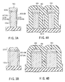
- the thin film 103b is etched vertically as shown in FIG. 3A.
- the metal film 103a is side-etched, and the thin film 103b overhangs the metal film 103a. If the thin film 103b overhangs, a void is likely to be caused between adjacent metal films 103a when the insulation film 105 is deposited, as shown in FIG. 4A.
- the side-etching of the metal film 103a is reduced as illustrated in FIG. 3B.
- the thin film 103b is not etched vertically but tapered, and its bottom portion is increased in size. If the bottom portion of the thin film 103b is increased in size, the metal film 103a is broadened, and a distance D between adjacent metal films 103a is narrowed as shown in FIG. 4B, with the result that fine metal wiring becomes difficult.
- the thin film 103b is etched partway by increasing the mixture ratio of the chlorine gas and then the metal film 103a is etched by decreasing it. If the mixture ratio is so changed partway, it is possible to obtain the advantages that the thin film 103b can be etched vertically and the side-etching of the metal film 103a can be prevented.
- the etching rate of the thin film 103b and metal film 103a is nonuniform within the plane of the semiconductor substrate. Consequently, the above advantages are difficult to obtain uniformly throughout the semiconductor substrate even though the mixture ratio of the chlorine gas is changed partway.
- the present invention has been developed in consideration of the above situation and its principal object is to provide a dry etching method capable of patterning a stacked film of a metal film and a thin film, formed on the metal film and including one of metal and a metal compound, in such a manner that the thin film is formed vertically and the metal film is prevented from being side-etched.
- a method of dry etching comprising: forming a mask layer on a stacked film above a semiconductor substrate, the stacked film including a metal film formed above the semiconductor substrate and containing aluminum as a base component and a thin film formed on the metal film and containing at least one of metal and a metal compound; and patterning the stacked film using the mask layer as a mask for etching, the patterning including: a first step of dry etching the thin film using a first etching gas having a gas composition for preventing the metal film from being processed; and a second step of dry etching the metal film using a second etching gas having a gas composition other than that of the first etching gas.
- Another object of the present invention is to provide a dry etching method capable of patterning a stacked film of a barrier layer and a metal film formed on the barrier layer so as to reduce a pattern transfer difference.
- a method of dry etching comprising: forming a mask layer on a stacked film above a semiconductor substrate, the stacked film including a barrier layer formed above the semiconductor substrate and a metal film formed on the barrier layer and containing aluminum as a base component; and patterning the stacked film using the mask layer as a mask for etching, the patterning including a step of dry etching the stacked film using an etching gas containing atoms of oxygen.
- FIG. 5 is a view schematically showing the dry etching apparatus of the present invention.
- the dry etching apparatus includes an inductively coupled plasma (ICP) coil 1.
- ICP inductively coupled plasma
- a reaction treating chamber 10 is made of an aluminum alloy and its inner wall is coated with an oxide film (anodized aluminum).
- a subject 5, such as a semiconductor wafer, which is to be processed, is placed on a lower electrode 2 and housed in the reaction treating chamber 10.
- the ICP coil 1 and lower electrode 2 are connected to a high-frequency power supply 7 via a blocking capacitor 6.
- the power supply 7 supplies high-frequency power to the ICP coil 1 and lower electrode 2.
- Reactive gas is introduced from a gas inlet port 3 into the reaction treating chamber 10 through a transparent hole 8 formed in a ceramic part (partition) 4.
- the dry etching method is used for patterning of metal wiring in the semiconductor device.
- FIG. 6 is a cross-sectional view of a semiconductor substrate on which metal wiring is carried out.
- an insulation film 12 is formed on a semiconductor substrate (wafer) 11.
- the semiconductor substrate 11 is constituted of a semiconductor such as silicon, while the insulation film 12 is formed of an insulator such as silicon oxide (SiO 2 ).
- the surface of the insulation film 12 is planarized, and metal wiring (stacked film) 13 is formed on the planarized surface of the insulation film 12.
- the metal wiring is electrically connected to its underlying wiring (not shown), the semiconductor substrate 11, the gate of a MOS transistor (not shown), or the like and also connected to its upper metal wiring (not shown) formed on an insulation film 18.
- the insulation film 18 is constituted of an insulator such as silicon oxide (SiO 2 ) and formed on the semiconductor substrate 11 so as to coat the metal wiring.
- the stacked film 13 includes a metal film 13a and a thin film 13b formed on the metal film 13a.
- the metal film 13a is an alloy including aluminum as the principal ingredient and containing copper and silicon as appropriate.
- the thin film 13b has a single-layer structure of metal or a metal compound for protecting the metal film 13a and improving the reliability of the wiring or a multilayer structure of the above metal and metal compound. Titanium and tungsten are selected as the metal, while titanium nitride and tungsten silicide are selected as the metal compound.
- FIG. 6 shows an example of a multilayer structure of the thin film 13b including a titanium layer (Ti layer) 14 formed on the metal film 13a and a titanium nitride (TiN layer) 15 formed on the Ti layer 14.
- the metal wiring of the stacked film 13 is formed by the steps shown in FIGS. 7A to 7E.
- FIGS. 7A to 7E are cross-sectional views showing a method of carrying out metal wiring using a dry etching method according to a first embodiment of the present invention.
- an insulation film is formed on a semiconductor substrate 11, and a metal film 13a containing aluminum as the base metal and a thin film 13b are sequentially stacked one on another on the insulation film 12 to form a stacked film 13.
- the thin film 13b includes a Ti layer 14 and a TiN layer 15.
- the first embodiment need not therefore include any reflection preventing films.
- photoresist is applied onto the stacked film 13 to form a photoresist film.
- a pattern corresponding to the metal wiring is formed on the photoresist film.
- the photoresist film is developed to form a photoresist pattern 17 having a metal wiring pattern.
- the structure shown in FIG. 7B is housed in the reaction treating chamber 10 of the dry etching apparatus shown in FIG. 5. Using the photoresist pattern 17 as a mask, the stacked film 13 is dry-etched.
- the thin film 13b is dry-etched using a first etching gas.
- the first etching gas has a gas composition in which the thin film 13b is etched almost vertically and the metal film 13a is hardly etched.
- the thin film 13b is thus etched almost vertically, as shown in FIG. 7C. Since the metal film 13a is hardly etched by the first etching gas, the dry etching of the stacked film 13 is stopped temporarily when the metal film 13a is exposed.
- the metal film 13a can thus be so constituted that it is hardly etched. For this reason, even though the etching rate of the thin film 13b is nonuniform within the plane of the semiconductor substrate (wafer), the etching becomes almost uniform all over the semiconductor substrate so as to expose the metal film 13a.
- the first etching gas is switched to a second etching gas having a gas composition other than that of the first etching gas.
- the metal film 13a is dry-etched using the second etching gas.
- the metal film 13a is hardly side-etched but etched vertically. Therefore, as shown in FIG. 7D, the side-etching of the metal film 13a is decreased, with the result that the stacked film 13 is formed in the metal wiring pattern.
- the photoresist pattern is eliminated and thus the metal wiring of the stacked film 13 is completed.
- the structure shown in FIG. 6 is then obtained by depositing an insulation film 18 on the semiconductor substrate 11.
- the thin film 13b is dry-etched using the first etching gas having a gas composition in which the thin film 13b is etched almost vertically and the metal film 13a is hardly etched. Even though the etching rate of the thin film 13b is nonuniform within the plane of the semiconductor substrate, the etching can be almost uniformed all over the semiconductor substrate such that the metal film 13a is exposed.
- the metal film 13a is dry-etched using the second etching gas and thus it is hardly side-etched but etched vertically.
- the metal wiring of the stacked film 13, which includes the thin film 13b etched almost vertically and the metal film 13a decreased in side-etching, can thus be obtained as illustrated in FIG. 8.
- the thin film 13b does not overhang the metal film 13a. For this reason, a void as shown in FIG. 4A is hard to cause when an insulation film 18 is deposited as shown in FIG. 9. Since, moreover, the thin film 13b is not tapered by etching, a distance D between adjacent metal films becomes difficult to narrow as illustrated in FIG. 9. In the first embodiment, the metal wiring shown in FIG. 8 can be uniformed all over the semiconductor substrate.
- the first etching gas includes fluorine (F).
- the thin film 13b contains titanium (Ti), while the metal film 13a contains aluminum (Al).
- the aluminum fluoride is not vaporized but deposited on the metal film 13a, thereby preventing the metal film 13a from being etched.
- the metal film 13a on which the aluminum fluoride is deposited is not etched immediately after it is exposed to gas for etching metal containing aluminum as the base metal, such as chlorine gas.
- the first etching gas can be constituted of a mixture of gas containing fluorine and gas containing chlorine. The use of such a mixture does not increase the etching rate of the thin film 13b.
- the number of atoms of chlorine contained in the mixture has only to be set smaller than that of atoms of fluorine.
- the mixture so regulated prevents aluminum contained in the metal film 13a from being combined with chlorine.
- the first etching gas there is a mixture of chlorine gas (Cl 2 gas), argon gas (Ar gas), and carbon tetrafluoride gas (CF 4 gas).
- This mixture is introduced into the reaction treating chamber 10 of the dry etching apparatus illustrated in FIG. 5.
- the Cl 2 gas, Ar gas, and CF 4 gas have flow rates of about 30 sccm, about 100 sccm, and 30 sccm or lower (favorably 10 sccm or higher and 30 sccm or lower), respectively.
- the stacked film 13 is dry-etched using the first etching gas as the above specific example where the internal pressure of the reaction treating chamber 10 is about 2 Pa and the temperature of the lower electrode 2 is about 40°C, the structure shown in FIG. 7C can be completed.
- FIG. 10 is a graph showing the dependence of the etching rate of the metal film 13a on the flow rate percentage of CF 4 gas.
- an ordinate represents an etching rate (any unit) of the metal film 13a and an abscissa indicates a flow rate percentage of CF 4 (CF 4 /CF 4 +Cl 2 )(%).
- the flow rate of Cl 2 gas is always set to 30 sccm.
- the etching rate for etching the metal film 13a is varied markedly.
- the flow rate percentage of CF 4 is 0%
- the etching for the metal film 13a advances greatly; however, its etching rate decreases quickly as the flow rate percentage of CF 4 increases.
- the etching of the metal film 13a is essentially stopped when the flow rate percentage is about 25%, and this state continues when the percentage is 25% or higher.
- the second etching gas contains chlorine (Cl) gas and boron trichloride (BCl 3 ) gas, and the percentage of Cl gas is lowered to prevent the metal film 13a from being side-etched.
- the second etching gas can be replaced with the gas described in the Background of the Invention with reference to FIG. 3B, can be employed.
- FIGS. 11A to 11C are cross-sectional views showing a method of forming metal wiring using a dry etching method according to a second embodiment of the present invention.
- FIG. 11A First the structure as shown in FIG. 11A is obtained by the method described above with reference to FIGS. 7A to 7C.
- the first etching gas in the first embodiment is switched to the second etching gas therein to dry-etch a metal film 13a.
- the dry etching is performed by switching a small selective ratio of photoresist to a large selective ratio thereof partway.
- gas containing fluorine (F) e.g., CF 4 gas
- F fluorine
- the number of atoms of fluorine is smaller than that of atoms of chlorine.
- the second etching gas of the second embodiment is considered to be the same as that of the first embodiment. If the metal film 13a is dry-etched using the second etching gas, the structure as shown in FIG. 11c is completed.
- the metal film 13a is dry-etched by switching the small selective ratio of photoresist to the large selective ratio thereof partway. Therefore, in the step of FIG. 11B, the constituting materials fly out of the photoresist pattern 17. These materials serve as a so-called source of a sidewall protection film for suppressing the side-etching of the metal film 13a. For this reason, the dry etching of the metal film 13a advances particularly in the initial stage so as to form the sidewall protection film on the sidewall of the metal film 13a.
- a slight undercut of the metal film 13a can be prevented from occurring near the interface between the metal film 13a and thin film 13b.
- the dry etching of the metal film 13a advances particularly in its initial stage such that aluminum fluoride is formed further on the sidewall of the metal film 13a.
- the advantage of suppressing the above slight undercut can be made greater.
- FIGS. 12A to 12C are cross-sectional views showing a method of forming metal wiring using a dry etching method according to a third embodiment of the present invention.
- an insulation film 12 is formed on a semiconductor substrate 11, and a metal film 13a including aluminum as the base metal, a thin film 13b, and a reflection preventing film 13c are sequentially stacked one on another on the insulation film 12 to form a stacked film 13'.
- the thin film 13b includes a Ti layer 14 and a TiN layer 15.
- the reflection preventing film 13c is formed of an organic compound film containing carbon.
- photoresist is applied onto the stacked film 13' to form a photoresist film.
- a pattern corresponding to the metal wiring is formed on the photoresist film.
- the photoresist film is developed to form a photoresist pattern 17 having a metal wiring pattern.
- the structure shown in FIG. 12B is housed in the reaction treating chamber 10 of the dry etching apparatus illustrated in FIG. 5.
- the stacked film 13' is dry-etched using the photoresist pattern 17 as a mask.
- the reflection preventing film 13c and thin film 13b are dry-etched using a first etching gas.
- the first etching gas has a gas composition in which the reflection preventing film 13c and thin film 13b are etched almost vertically and the metal film 13a is hardly etched. As shown in FIG. 12C, therefore, the reflection preventing film 13a and thin film 13b are etched almost vertically. Since the metal film 13a is hardly etched by the first etching gas, the dry etching of the stacked film 13' is stopped temporarily when the metal film 13a is exposed. The metal film 13a can thus be so constituted that it is hardly etched.
- both the films 13b and 13c have only to be dry-etched using the first etching gas.
- the metal wiring formed in the foregoing first to third embodiments has a favorable shape, especially in a very fine lines-and-spaces (L/S) pattern region.
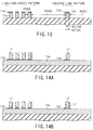
- the thin film 13b in an isolated line pattern region is etched more quickly than that in the L/S pattern region by the micro-loading effect. Therefore, the etching stops in the metal film 13a in the isolated line pattern region longer than that in the L/S pattern region.
- a decomposed object 17' of resist is deposited on the sidewall of the photoresist pattern 17 in the isolated line pattern region when the etching of the thin film 13b is completed.
- the metal wiring in the isolated line pattern region becomes wider than the design value, as shown FIG. 13.
- the size of the photoresist pattern 17 in the isolated line pattern region is adjusted in advance.
- the metal wiring in the isolated line pattern region can be formed in the same size as that of the metal wiring in the L/S pattern region.
- a dry etching method capable of patterning a stacked film of a metal film and a thin film, which includes metal or a metal compound and is formed on the metal film, in such a manner that the thin film is formed vertically and the metal film is prevented from being side-etched.
- the first to third embodiments are each directed to a method of dry etching a stacked film of both a metal film containing aluminum as the base metal and metal, a metal compound, or a thin film having a stacked structure of metal and metal compound, which is formed on the top of the metal film.
- the fourth embodiment is directed to a method of dry etching a stacked film of a metal film containing aluminum as the base metal and a thin film formed on the underside of the metal film.
- this thin film is referred to as a barrier layer.
- FIG. 15 is a cross-sectional view of a semiconductor substrate on which metal wiring is formed.
- the structure shown in FIG. 15 differs from that shown in FIG. 6 in that a barrier layer 13d is formed between an insulation film 12 and a metal film 13a.
- the metal wiring of the fourth embodiment is therefore constituted of a stacked film 13-2 of the barrier layer 13d, metal film 13a and thin film 13b.
- the metal film 13a is an alloy including aluminum as the principal ingredient and containing copper and silicon as appropriate.
- the thin film 13b has a single-layer structure of metal or a metal compound for protecting the metal film 13a and improving the reliability of the wiring, or a multilayer structure of the above metal and metal compound.
- the barrier layer 13d prevents the aluminum included in the metal film 13a from reacting on the metal wiring and semiconductor substrate 11 when the metal wiring is bonded to its lower wiring and the substrate 11.
- the barrier layer 13d therefore has a single-layer structure of metal such as titanium or a metal compound such as titanium nitride or a multilayer structure of the above metal and metal compound.
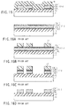
- the metal wiring of the stacked film 13-2 is formed by the steps illustrated in FIGS. 16A to 16D.
- an insulation film 12 is formed on a semiconductor substrate 12, and a barrier layer 13d, a metal film 13a, a thin film 13b and a reflection preventing film 13c are stacked one on another on the insulation film 12 to form a stacked film 13'-2.
- photoresist is applied onto the reflection preventing film 13c to form a photoresist film.
- a pattern corresponding to the metal wiring is formed on the photoresist film.
- This photoresist film is developed to form a photoresist pattern 17 having a metal wiring pattern.
- the stacked film 13'-2 is dry-etched using the photoresist pattern 17 as a mask, as shown in FIG. 16C.
- the photoresist pattern 17 and reflection preventing film 13c are removed to form metal wiring of a stacked film 13-2 including the barrier layer 13d, metal film 13a and thin film 13b.
- an insulation film 18 is deposited on the semiconductor substrate 11 as shown in FIG. 15.
- the metal wiring of the stacked film 13-2 is thus formed by patterning the stacked film 13'-2 including the barrier layer 13d, metal film 13a, thin film 13b, and reflection preventing film 13c. For this reason, these different metal films have to be processed continuously at the time of dry etching for the patterning.
- the width of a processed wiring portion becomes larger than that of a mask when a mask pattern (photoresist pattern 17) is formed on the stacked film 13-2 and then the stacked film 13-2 is processed by the dry etching method. In this case, it is likely that an interval between wiring portions will be narrowed and a short circuit will be caused easily between them. It is also likely that the wiring capacitance will increase and the device characteristics will deteriorate.
- a pattern transfer difference was measured in advance, and part of wiring was thinned only by the measured pattern transfer difference by controlling an amount of light exposure when a mask was formed, or an exposure mask was formed in advance taking into consideration the pattern transfer difference.
- the pattern transfer difference which is caused at the time of dry etching, is corrected by the mask pattern, the aspect ratio will be increased further and the mask pattern will be much easier to fall.
- the causes of the pattern transfer difference are that the metal film 13a is tapered and the processed barrier layer 13d is shaped such that its bottom expands.
- the vertical processing of the metal film 13a can be attained by optimizing processing conditions, gas composition, pressure, temperature, and the like. Under the present circumstances, however, it is difficult to process the barrier layer 13d underlying the metal film 13a in accordance with a mask size.
- the fourth embodiment aims at providing a dry etching method capable of etching a stacked film including a barrier layer 13d and a metal film 13a formed on the barrier layer 13d so as to reduce in pattern transfer difference.
- the inventors of the present invention conducted the following experiment in order to know how the bottom of the barrier layer 13d expanded.
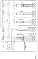
- FIG. 17 is a table showing results of the experiment.
- a stacked film 13-3 was dry-etched using a photoresist pattern 17-3 as a mask, and the mask sizes were measured in the respective steps.
- the stacked film 13-3 includes a TiN/Ti film serving as a barrier layer 13d, an Al-Cu film (Cu content of 1 wt%) serving as a metal film 13a containing aluminum as the base metal, and a TiN film serving as a reflection preventing film 13c.
- a mixture of Cl 2 +BCl 3 was used as an etching gas.
- mask size S hardly varied during the processing of Al-Cu film (during the processing of Al, i.e., state b ) but changed abruptly after an Al end-point indicating the completion of processing of Al-Cu film, as shown in FIG. 17.
- the Al end-point was set where the monitored 261-nm light emission intensity of plasma was decreased to 80% of the maximum. In other words, the processing of part of an Al-Cu film on a semiconductor substrate to be processed had been completed when the Al end-point was detected, but the processing of the remaining part had not been completed (state c ).
- the inventors checked a variation in resist film thickness H in each etching step in order to find a reason for which the mask size was increased after the Al end point is detected. Results of this are also shown in FIG. 17.
- the processing of part of the Al-Cu film is completed and the barrier layer 13d is exposed.
- the processing area of the Al-Cu film is decreased and thus the Cl gas (activated species) to be consumed for processing the Al-Cu film is left and the etching rate of photoresist is increased.
- the etched photoresist is exhausted in the form of CCl 4 ; however, it is decomposed again in plasma and deposited on the semiconductor substrate to be treated or on the mask.
- the decomposed objects deposited on the top and sidewall of the mask are etched by ions.
- the etching rate at which the decomposed object is removed by etching from the sidewall of the mask is lower than the speed at which the decomposed object is deposited thereon. It is thus thought that the mask size is increased. This tendency becomes more conspicuous after the processing of the barrier layer 13d and the exposure of an oxide film 12-3.
- FIG. 18 is a graph showing a relationship between the flow rate of oxygen added to the etching gas after the Al end-point and the mask size S.
- the ordinate indicates the mask size S ( ⁇ m)
- the abscissa represents the flow rate (sccm) of oxygen added to the etching gas.
- mask size S was prevented from increasing as the oxygen flow rate increases.
- oxygen was added after the Al end-point.
- the mask size S was not decreased. The reason is as follows. If an amount of oxygen to be added is small, the oxygen does not contribute to the etching of deposits and most oxygen contributes to scavenging of carbon caused by re-decompression of photoresist in plasma.
- the mask size S starts to decrease.
- oxygen can be added from the beginning if the amount of oxygen to be added is larger than a given limit.
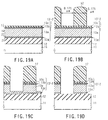
- FIGS. 19A to 19D are cross-sectional views showing a method of carrying out metal wiring using a dry etching method according to the fourth embodiment of the present invention.
- an insulation film 12 is formed on a semiconductor substrate 11.
- the insulation film 12 is constituted of silicon oxide (SiO 2 ) and its surface is planarized.
- a barrier layer 13d is formed on the insulation film 12.
- the barrier layer 13d has a stacked structure of a Ti film 21 formed on the insulation film 12 and having a thickness of about 10 nm and a TiN film 22 formed on the Ti film 21 and having a thickness of about 40 nm.
- a metal film 13a is formed on the barrier layer 13d.
- the metal film 13a is constituted of an alloy formed on the TiN film 22 and having a thickness of about 330 nm.
- the alloy includes aluminum as the base metal and contains copper (Cu) of about 1 wt%.
- a thin film 13b is formed on the metal film 13a.
- the thin film 13b has a stacked structure of a Ti film 14 formed on the metal film 13a and having a thickness of 10 nm and a TiN film 15 formed on the Ti film 14 and having a thickness of 50 nm.
- a reflection preventing film 13c is formed on the thin film 13b.
- the reflection preventing film 13c is constituted of a carbon-containing organic compound.
- a stacked film 13'-2 of the barrier layer 13d, metal film 13a, thin film 13b, and reflection preventing film 13c is formed on the insulation film 12.
- photoresist is applied onto the reflection preventing film 13c to form a photoresist film.
- a pattern corresponding to the metal wiring is formed on the photoresist film.
- the photoresist film is developed to form a photoresist pattern 17 having a metal wiring pattern.
- the wiring line and space are both 0.175 ⁇ m.
- the structure shown in FIG. 19B is housed in the reaction chamber 10 of the dry etching apparatus shown in FIG. 5. Using the photoresist pattern 17 as a mask, the stacked film 13'-2 is dry-etched.
- the stacked film 13'-2 is etched in two steps, i.e., before the Al end-point (main etching) and after the Al end-point (over-etching).
- the Al end-point is set where monitored 261-nm light emission intensity of plasma is decreased to 80% of the maximum.
- the processing of part of the metal film 13a is completed, but that of the remaining part thereof is not completed.
- etching gas a mixture of Cl 2 , BCL 3 and N 2 is employed as an etching gas.
- the ratio of Cl 2 /BCL 3 /N 2 is, for example, 80/70/5 sccm.
- pressure is 12 mTorr
- substrate treatment temperature is 35°C
- power applied to a coil 1 is 500w
- bias power applied to a lower electrode 2 is 350W. The main etching is thus completed to obtain the structure shown in FIG. 19C.
- etching gas a mixture of Cl 2 , BCL 3 , N 2 and O 2 is employed as an etching gas.
- the ratio of Cl 2 /BCL 3 /N 2 /O 2 is, for example, 60/40/5/2 sccm.
- pressure is 12 mTorr
- substrate treatment temperature is 35°C
- power applied to a coil 1 is 350W
- bias power applied to the lower electrode 2 is 200W.
- oxygen (O 2 ) of 2 sccm is added to the etching gas used for the over-etching.
- the over-etching is completed to obtain the structure shown in FIG. 19D.
- FIG. 20 A section of metal wiring formed by the dry etching method according to the above fourth embodiment, is illustrated in FIG. 20.
- the barrier layer 13d is simply increased about 0.04 ⁇ m (0.02 ⁇ m in each of right and left directions) from the mask size S (0.175 ⁇ m).
- the comparative example differs from the method according to the fourth embodiment particularly in that oxygen (O 2 ) is not added to the etching gas used for the over-etching.
- the etching gas and etching condition for the main etching of the comparative example are the same as those of the fourth embodiment.
- etching a mixture of Cl 2 /BCL 3 /N 2 of 60/40/5 sccm is employed.
- pressure is 12 mTorr
- substrate treatment temperature is 35°C
- power applied to a coil is 350W
- bias power applied to the lower electrode is 200W.
- FIG. 21 A section of metal wiring formed by the dry etching method according to the comparative example, is illustrated in FIG. 21.
- the barrier layer 13d is simply increased about 0.08 ⁇ m (0.04 ⁇ m in each of right and left directions) from the mask size S (0.175 ⁇ m).
- the dry etching method according to the fourth embodiment allows a pattern transfer difference to decrease to 0.02 ⁇ m in each of right and left directions. It is thus possible to suppress the phenomenon in which the processed barrier layer 13d is shaped such that its bottom expands.
- a fifth embodiment of the present invention is directed to a method of dry etching a stacked film of a barrier layer, a metal film formed on the barrier layer and containing aluminum as the principal ingredient, and a thin film formed on the metal film.
- FIGS. 22A to 22D are cross-sectional views showing a method of carrying out metal wiring employing a dry etching method according to the fifth embodiment of the present invention.
- FIG. 22A The structure illustrated in FIG. 22A is obtained by the method described with reference to FIGS. 19A and 19B.
- a reflecting prevention film 13c is formed, but it is needless to say that the film 13c need not be formed.
- a reflection preventing film 13c and a thin film 13b are dry-etched using a first etching gas by the method according to the third embodiment of the present invention.
- the first etching gas has a gas composition in which the reflection preventing film 13c and thin film 13b are etched almost vertically and a metal film 13a is hardly etched.
- the first etching gas contains Cl 2 gas, A r gas and CF 4 gas.
- the flow-rate ratio of Cl 2 /Ar/CF 4 is 30/100/30 or less (favorably 10 ⁇ CF 4 ⁇ 30) sccm.
- the first etching gas is switched to a second etching gas, and the metal film 13a is dry-etched using the second etching gas.
- the second etching gas has a gas composition in which the metal film 13a is hardly side-etched but etched vertically.
- the second etching gas includes Cl 2 gas and BCL 3 gas and specifically it can be replaced with the mixture in the fourth embodiment of the present invention.
- the metal film 13a containing aluminum as the base metal is dry-etched to the Al end-point. This process corresponds to the main etching described in the fourth embodiment.
- the structure shown in FIG. 22C is thus obtained.
- the second etching gas is switched to a third etching gas, and a barrier layer 13d is dry-etched using the third etching gas.
- the third etching gas has a gas composition in which an etching product is prevented from being deposited excessively on the sidewall of a photoresist pattern 17.
- the third etching gas includes Cl 2 gas, BCL 3 gas, N 2 gas, and O 2 gas.
- the flow-rate ratio of Cl 2 /BCL 3 /N 2 /O 2 is 60/40/5/2 sccm.
- the barrier layer 13d is dry-etched using the third etching gas. This process corresponds to the over-etching described in the fourth embodiment. Thus, the structure shown in FIG. 22D is obtained.
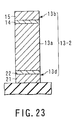
- FIG. 23 A section of metal wiring formed by the dry etching method according to the fifth embodiment, is illustrated in FIG. 23.
- the thin film 13b can be etched vertically, while the metal film 13a can be etched so as to suppress its side-etching.
- the barrier layer 13d can be etched so as to prevent its bottom from expanding.
- the main etching is switched to the over-etching based on the Al end-point.
- this switching can be done based on processing time.
- the dry etching method of the second embodiment can be applied to the main etching of the fifth embodiment.
- the thin film 13b and barrier layer 13d each have a stacked structure. However, they can have a single layer structure of titanium, tungsten, titanium nitride, or tungsten silicide.
Landscapes
- Chemical & Material Sciences (AREA)
- Engineering & Computer Science (AREA)
- Materials Engineering (AREA)
- Mechanical Engineering (AREA)
- Metallurgy (AREA)
- Organic Chemistry (AREA)
- Drying Of Semiconductors (AREA)
- Internal Circuitry In Semiconductor Integrated Circuit Devices (AREA)
Abstract
Description
Claims (19)
- A method of dry etching comprising:forming a mask layer (17) on a stacked film (13) above a semiconductor substrate (11), the stacked film (13) including a metal film (13a) formed above the semiconductor substrate (11) and containing aluminum as a base component and a thin film (13b) formed on the metal film (13a) and containing at least one of metal and a metal compound; andpatterning the stacked film (13) using the mask layer (17) as a mask for etching,
characterized in that the patterning includes a first step of dry etching the thin film (13b) using a first etching gas having a gas composition for preventing the metal film (13a) from being processed and a second step of dry etching the metal film (13a) using a second etching gas having a gas composition other than that of the first etching gas. - A method of dry etching comprising:forming a mask layer (17) on a stacked film (13') above a semiconductor substrate (11), the stacked film (13') including a metal film (13a) formed above the semiconductor substrate (11) and containing aluminum as a base component, a thin film (13b) formed on the metal film (13a) and containing at least one of metal and a metal compound, and a reflection preventing film (13c) formed on the thin film (13b); andpatterning the stacked film (13) using the mask layer (17) as a mask for etching,
characterized in that the patterning includes a first step of dry etching the reflection preventing film (13c) and the thin film (13b) using a first etching gas having a gas composition for preventing the metal film (13a) from being processed and a second step of dry etching the metal film (13a) using a second etching gas having a gas composition other than that of the first etching gas. - The method of dry etching according to one of claim 1 and claim 2, characterized in that wherein the thin film (13b) includes at least one of titanium, tungsten, titanium nitride, and tungsten silicide.
- The method of dry etching according to any one of claim 1 to claim 3, characterized in that the metal film (13a) contains at least one of copper and silicon.
- The method of dry etching according to any one of claim 1 to claim 4, characterized in that the first etching gas includes atoms of fluorine.
- The method of dry etching according to claim 5, characterized in that the first etching gas includes a carbon tetrafluoride gas and a chlorine gas, and a flow rate percentage of the carbon tetrafluoride gas is 25% or more.
- The method of dry etching according to any one of claim 1 to claim 6, characterized in that the second step is executed first under a first condition in which a selective ratio for the mask layer is small and then under a second condition in which the selective ratio is large.
- The method of dry etching according to claim 7, characterized in that the second etching gas includes atoms of chlorine and atoms of fluorine, which are fewer than the atoms of chlorine, in the first condition.
- A method of dry etching comprising:forming a mask layer (17) on a stacked film (13'-2) above a semiconductor substrate (11), the stacked film (13) including a barrier layer (13d) formed above the semiconductor substrate (11) and a metal film (13a) formed on the barrier layer (13d) and containing aluminum as a base component; andpatterning the stacked film (1) using the mask layer (17) as a mask for etching,
characterized in that the patterning includes a step of dry etching the stacked film (13'-2) using an etching gas containing atoms of oxygen. - A method of dry etching comprising:forming a mask layer (17) on a stacked film (13'-2) above a semiconductor substrate (11), the stacked film (13'-2) including a barrier layer (13d) formed above the semiconductor substrate (11), a metal film (13a) formed on the barrier layer (13d) and containing aluminum as a base component, and a thin film (13b) formed on the metal film (13a) and including at least one of metal and a metal compound; andpatterning the stacked film (13'-2) using the mask layer (17) as a mask for etching,
characterized in that the patterning includes a step of dry etching the stacked film (13'-2) using an etching gas containing atoms of oxygen. - A method of dry etching comprising:forming a mask layer (17) on a stacked film (13'-2) above a semiconductor substrate (11), the stacked film (13'-2) including a barrier layer (13d) formed above the semiconductor substrate (11), a metal film (13a) formed on the barrier layer (13d) and containing aluminum as a base component, a thin film (13b) formed on the metal film (13a) and including at least one of metal and a metal compound, and a reflection preventing film (13c) formed on the thin film (13b); andpatterning the stacked film (13'-2) using the mask layer (17) as a mask for etching,
characterized in that the patterning includes a step of dry etching the stacked film (13'-2) using an etching gas containing atoms of oxygen. - The method of dry etching according to any one of claim 9 to claim 11, characterized in that the etching gas is used after part of the barrier layer is exposed.
- The method of dry etching according to any one of claim 9 to claim 12, characterized in that the barrier layer (13d) includes at least one of titanium, tungsten, titanium nitride, and tungsten silicide.
- The method of dry etching according to any one of claim 9 to claim 13, characterized in that the metal film (13a) contains at least one of copper and silicon.
- The method of dry etching according to any one of claim 9 to claim 14, characterized in that the etching gas includes at least one of an oxygen gas, a carbon monoxide gas, and a carbon dioxide gas.
- The method of dry etching according to any one of claim 9 to claim 15, characterized in that the etching gas includes oxygen of 2 sccm or more.
- A method of dry etching comprising:forming a mask layer (17) on a stacked film (13'-2) above a semiconductor substrate (11), the stacked film (13'-2) including a barrier layer (13d) formed above the semiconductor substrate (11), a metal film (13a) formed on the barrier layer (13d) and containing aluminum as a base component, and a thin film (13b) formed on the metal film (13a) and including at least one of metal and a metal compound; andpatterning the stacked film (13'-2) using the mask layer (17) as a mask for etching,
characterized in that the patterning includes a first step of dry etching the thin film (13b) using a first etching gas having a gas composition for preventing the metal film (13a) from being processed, a second step of dry etching the metal film (13a) using a second etching gas having a gas composition other than that of the first etching gas and a third step of dry etching the barrier layer (13d) using a third etching gas containing atoms of oxygen. - The method of dry etching according to claim 17, characterized in that the first etching gas includes an argon gas, a chlorine gas, and a carbon tetrafluoride gas of 30 sccm or less, the second etching gas includes a chlorine gas and a boron trichloride, and the third etching gas includes oxygen of 2 sccm or more.
- The method of dry etching according to one of claim 17 and claim 18, characterized in that the first etching gas includes atoms of fluorine.
Applications Claiming Priority (4)
| Application Number | Priority Date | Filing Date | Title |
|---|---|---|---|
| JP11065046A JP2000260759A (en) | 1999-03-11 | 1999-03-11 | Dry etching method |
| JP6504699 | 1999-03-11 | ||
| JP11068052A JP2000269188A (en) | 1999-03-15 | 1999-03-15 | Dry etching method |
| JP6805299 | 1999-03-15 |
Publications (2)
| Publication Number | Publication Date |
|---|---|
| EP1035570A2 true EP1035570A2 (en) | 2000-09-13 |
| EP1035570A3 EP1035570A3 (en) | 2003-01-02 |
Family
ID=26406188
Family Applications (1)
| Application Number | Title | Priority Date | Filing Date |
|---|---|---|---|
| EP00104520A Withdrawn EP1035570A3 (en) | 1999-03-11 | 2000-03-10 | Dry etching method |
Country Status (5)
| Country | Link |
|---|---|
| US (1) | US6383942B1 (en) |
| EP (1) | EP1035570A3 (en) |
| KR (1) | KR100363591B1 (en) |
| CN (1) | CN1135606C (en) |
| TW (1) | TW448503B (en) |
Cited By (1)
| Publication number | Priority date | Publication date | Assignee | Title |
|---|---|---|---|---|
| WO2002015231A3 (en) * | 2000-08-14 | 2002-11-07 | Motorola Inc | A method for patterning layers of semiconductor devices |
Families Citing this family (18)
| Publication number | Priority date | Publication date | Assignee | Title |
|---|---|---|---|---|
| US6333272B1 (en) * | 2000-10-06 | 2001-12-25 | Lam Research Corporation | Gas distribution apparatus for semiconductor processing |
| US6589868B2 (en) * | 2001-02-08 | 2003-07-08 | Applied Materials, Inc. | Si seasoning to reduce particles, extend clean frequency, block mobile ions and increase chamber throughput |
| US6511911B1 (en) | 2001-04-03 | 2003-01-28 | Advanced Micro Devices, Inc. | Metal gate stack with etch stop layer |
| TW582071B (en) * | 2001-03-20 | 2004-04-01 | Macronix Int Co Ltd | Method for etching metal in a semiconductor |
| US6770214B2 (en) * | 2001-03-30 | 2004-08-03 | Lam Research Corporation | Method of reducing aluminum fluoride deposits in plasma etch reactor |
| KR100422021B1 (en) * | 2001-06-16 | 2004-03-12 | (주)울텍 | Dry Etching Process of transition metal thin film |
| WO2003019590A1 (en) * | 2001-08-21 | 2003-03-06 | Seagate Technology Llc | Enhanced ion beam etch selectivity of magnetic thin films using carbon-based gases |
| US7190008B2 (en) * | 2002-04-24 | 2007-03-13 | E Ink Corporation | Electro-optic displays, and components for use therein |
| KR20040001487A (en) * | 2002-06-28 | 2004-01-07 | 주식회사 하이닉스반도체 | emthod for etching metal layer |
| KR100928098B1 (en) * | 2002-12-24 | 2009-11-24 | 동부일렉트로닉스 주식회사 | Metal line formation method using oxide film |
| KR100541152B1 (en) * | 2003-07-18 | 2006-01-11 | 매그나칩 반도체 유한회사 | Metal wiring layer formation method of a semiconductor device |
| JP4908824B2 (en) * | 2005-11-11 | 2012-04-04 | ローム株式会社 | Manufacturing method of semiconductor device |
| KR101316634B1 (en) * | 2006-09-29 | 2013-10-15 | 삼성디스플레이 주식회사 | Method of forming metal line and method of manufacturing a display substrate by using the same |
| KR100925210B1 (en) * | 2008-05-27 | 2009-11-06 | 한국전자통신연구원 | Method of manufacturing oxide thin film transistor using dry etching process |
| WO2014094103A1 (en) * | 2012-12-18 | 2014-06-26 | Seastar Chemicals Inc. | Process and method for in-situ dry cleaning of thin film deposition reactors and thin film layers |
| JP2015046459A (en) * | 2013-08-28 | 2015-03-12 | ソニー株式会社 | Etching method, method of manufacturing electronic device, and method of manufacturing polarizing device |
| CN108919407A (en) * | 2018-07-11 | 2018-11-30 | 京东方科技集团股份有限公司 | The preparation method and wire grid polarizer of metal wire and wire grating, electronic device |
| CN119208469B (en) * | 2024-09-27 | 2025-10-10 | 广东中图半导体科技股份有限公司 | Semiconductor substrate etching method |
Family Cites Families (11)
| Publication number | Priority date | Publication date | Assignee | Title |
|---|---|---|---|---|
| US5045150A (en) * | 1986-09-11 | 1991-09-03 | National Semiconductor Corp. | Plasma etching using a bilayer mask |
| JPH0235731A (en) * | 1988-07-26 | 1990-02-06 | Seiko Epson Corp | Manufacturing method of semiconductor device |
| US4915779A (en) * | 1988-08-23 | 1990-04-10 | Motorola Inc. | Residue-free plasma etch of high temperature AlCu |
| US5326427A (en) * | 1992-09-11 | 1994-07-05 | Lsi Logic Corporation | Method of selectively etching titanium-containing materials on a semiconductor wafer using remote plasma generation |
| JPH06104217A (en) * | 1992-09-18 | 1994-04-15 | Hitachi Ltd | Etching method |
| JPH0774156A (en) | 1993-08-31 | 1995-03-17 | Nec Corp | Manufacture of semiconductor device |
| JPH08274077A (en) | 1995-03-31 | 1996-10-18 | Sony Corp | Plasma etching method |
| US5952244A (en) * | 1996-02-15 | 1999-09-14 | Lam Research Corporation | Methods for reducing etch rate loading while etching through a titanium nitride anti-reflective layer and an aluminum-based metallization layer |
| US5846443A (en) * | 1996-07-09 | 1998-12-08 | Lam Research Corporation | Methods and apparatus for etching semiconductor wafers and layers thereof |
| US5883007A (en) * | 1996-12-20 | 1999-03-16 | Lam Research Corporation | Methods and apparatuses for improving photoresist selectivity and reducing etch rate loading |
| US5846884A (en) * | 1997-06-20 | 1998-12-08 | Siemens Aktiengesellschaft | Methods for metal etching with reduced sidewall build up during integrated circuit manufacturing |
-
2000
- 2000-03-06 TW TW089103984A patent/TW448503B/en not_active IP Right Cessation
- 2000-03-09 KR KR1020000011754A patent/KR100363591B1/en not_active Expired - Fee Related
- 2000-03-09 US US09/522,168 patent/US6383942B1/en not_active Expired - Fee Related
- 2000-03-10 EP EP00104520A patent/EP1035570A3/en not_active Withdrawn
- 2000-03-10 CN CNB001068849A patent/CN1135606C/en not_active Expired - Fee Related
Cited By (1)
| Publication number | Priority date | Publication date | Assignee | Title |
|---|---|---|---|---|
| WO2002015231A3 (en) * | 2000-08-14 | 2002-11-07 | Motorola Inc | A method for patterning layers of semiconductor devices |
Also Published As
| Publication number | Publication date |
|---|---|
| EP1035570A3 (en) | 2003-01-02 |
| CN1135606C (en) | 2004-01-21 |
| US6383942B1 (en) | 2002-05-07 |
| KR20000076800A (en) | 2000-12-26 |
| KR100363591B1 (en) | 2002-12-05 |
| TW448503B (en) | 2001-08-01 |
| CN1267905A (en) | 2000-09-27 |
Similar Documents
| Publication | Publication Date | Title |
|---|---|---|
| US6383942B1 (en) | Dry etching method | |
| EP0880799B1 (en) | Methods for etching semiconductor wafers | |
| US5486492A (en) | Method of forming multilayered wiring structure in semiconductor device | |
| JP2003100871A (en) | Dual hard mask method for forming copper / low k wiring | |
| JP2001156170A (en) | Manufacturing method of multilayer wiring | |
| JPH1171689A (en) | Method for etching selected portions of a laminate in a plasma processing chamber and reducing sidewall polymer deposition during etching | |
| US6046114A (en) | Method for producing a semiconductor device | |
| US6271115B1 (en) | Post metal etch photoresist strip method | |
| KR100581244B1 (en) | Fabricating method of semiconductor device | |
| JP2891952B2 (en) | Method for manufacturing semiconductor device | |
| JPH07147271A (en) | Method for manufacturing semiconductor device | |
| JP3112832B2 (en) | Method for manufacturing semiconductor device | |
| US5741742A (en) | Formation of aluminum-alloy pattern | |
| JP2022544026A (en) | How to use ultra-thin ruthenium metal hardmasks for etch profile control | |
| JP3238563B2 (en) | Method for manufacturing semiconductor device | |
| JP2001284327A (en) | Dry etching method, semiconductor device manufacturing method, and semiconductor device | |
| JPH10209276A (en) | Wiring formation method | |
| JPH0922881A (en) | Contact plug formation method | |
| JPH08186120A (en) | Manufacture of semiconductor device | |
| JP2000269188A (en) | Dry etching method | |
| JPH11135481A (en) | Etching method | |
| JPH05121378A (en) | Method for manufacturing semiconductor device | |
| JP3780657B2 (en) | Etching method | |
| JPH08339987A (en) | Wiring formation method | |
| JP3475666B2 (en) | Dry etching method |
Legal Events
| Date | Code | Title | Description |
|---|---|---|---|
| PUAI | Public reference made under article 153(3) epc to a published international application that has entered the european phase |
Free format text: ORIGINAL CODE: 0009012 |
|
| 17P | Request for examination filed |
Effective date: 20000310 |
|
| AK | Designated contracting states |
Kind code of ref document: A2 Designated state(s): AT BE CH CY DE DK ES FI FR GB GR IE IT LI LU MC NL PT SE |
|
| AX | Request for extension of the european patent |
Free format text: AL;LT;LV;MK;RO;SI |
|
| PUAL | Search report despatched |
Free format text: ORIGINAL CODE: 0009013 |
|
| AK | Designated contracting states |
Kind code of ref document: A3 Designated state(s): AT BE CH CY DE DK ES FI FR GB GR IE IT LI LU MC NL PT SE |
|
| AX | Request for extension of the european patent |
Free format text: AL;LT;LV;MK;RO;SI |
|
| AKX | Designation fees paid |
Designated state(s): DE FR GB |
|
| 17Q | First examination report despatched |
Effective date: 20050119 |
|
| STAA | Information on the status of an ep patent application or granted ep patent |
Free format text: STATUS: THE APPLICATION IS DEEMED TO BE WITHDRAWN |
|
| 18D | Application deemed to be withdrawn |
Effective date: 20050530 |