JP2015046459A - Etching method, method of manufacturing electronic device, and method of manufacturing polarizing device - Google Patents
Etching method, method of manufacturing electronic device, and method of manufacturing polarizing device Download PDFInfo
- Publication number
- JP2015046459A JP2015046459A JP2013176347A JP2013176347A JP2015046459A JP 2015046459 A JP2015046459 A JP 2015046459A JP 2013176347 A JP2013176347 A JP 2013176347A JP 2013176347 A JP2013176347 A JP 2013176347A JP 2015046459 A JP2015046459 A JP 2015046459A
- Authority
- JP
- Japan
- Prior art keywords
- region
- film
- metal film
- etching
- formation region
- Prior art date
- Legal status (The legal status is an assumption and is not a legal conclusion. Google has not performed a legal analysis and makes no representation as to the accuracy of the status listed.)
- Pending
Links
Images


Classifications
-
- G—PHYSICS
- G02—OPTICS
- G02B—OPTICAL ELEMENTS, SYSTEMS OR APPARATUS
- G02B5/00—Optical elements other than lenses
- G02B5/30—Polarising elements
- G02B5/3025—Polarisers, i.e. arrangements capable of producing a definite output polarisation state from an unpolarised input state
-
- C—CHEMISTRY; METALLURGY
- C23—COATING METALLIC MATERIAL; COATING MATERIAL WITH METALLIC MATERIAL; CHEMICAL SURFACE TREATMENT; DIFFUSION TREATMENT OF METALLIC MATERIAL; COATING BY VACUUM EVAPORATION, BY SPUTTERING, BY ION IMPLANTATION OR BY CHEMICAL VAPOUR DEPOSITION, IN GENERAL; INHIBITING CORROSION OF METALLIC MATERIAL OR INCRUSTATION IN GENERAL
- C23F—NON-MECHANICAL REMOVAL OF METALLIC MATERIAL FROM SURFACE; INHIBITING CORROSION OF METALLIC MATERIAL OR INCRUSTATION IN GENERAL; MULTI-STEP PROCESSES FOR SURFACE TREATMENT OF METALLIC MATERIAL INVOLVING AT LEAST ONE PROCESS PROVIDED FOR IN CLASS C23 AND AT LEAST ONE PROCESS COVERED BY SUBCLASS C21D OR C22F OR CLASS C25
- C23F4/00—Processes for removing metallic material from surfaces, not provided for in group C23F1/00 or C23F3/00
-
- G—PHYSICS
- G02—OPTICS
- G02B—OPTICAL ELEMENTS, SYSTEMS OR APPARATUS
- G02B5/00—Optical elements other than lenses
- G02B5/30—Polarising elements
- G02B5/3025—Polarisers, i.e. arrangements capable of producing a definite output polarisation state from an unpolarised input state
- G02B5/3058—Polarisers, i.e. arrangements capable of producing a definite output polarisation state from an unpolarised input state comprising electrically conductive elements, e.g. wire grids, conductive particles
-
- H—ELECTRICITY
- H05—ELECTRIC TECHNIQUES NOT OTHERWISE PROVIDED FOR
- H05K—PRINTED CIRCUITS; CASINGS OR CONSTRUCTIONAL DETAILS OF ELECTRIC APPARATUS; MANUFACTURE OF ASSEMBLAGES OF ELECTRICAL COMPONENTS
- H05K3/00—Apparatus or processes for manufacturing printed circuits
- H05K3/02—Apparatus or processes for manufacturing printed circuits in which the conductive material is applied to the surface of the insulating support and is thereafter removed from such areas of the surface which are not intended for current conducting or shielding
- H05K3/06—Apparatus or processes for manufacturing printed circuits in which the conductive material is applied to the surface of the insulating support and is thereafter removed from such areas of the surface which are not intended for current conducting or shielding the conductive material being removed chemically or electrolytically, e.g. by photo-etch process
- H05K3/061—Etching masks
-
- H—ELECTRICITY
- H05—ELECTRIC TECHNIQUES NOT OTHERWISE PROVIDED FOR
- H05K—PRINTED CIRCUITS; CASINGS OR CONSTRUCTIONAL DETAILS OF ELECTRIC APPARATUS; MANUFACTURE OF ASSEMBLAGES OF ELECTRICAL COMPONENTS
- H05K2203/00—Indexing scheme relating to apparatus or processes for manufacturing printed circuits covered by H05K3/00
- H05K2203/05—Patterning and lithography; Masks; Details of resist
- H05K2203/0562—Details of resist
- H05K2203/058—Additional resists used for the same purpose but in different areas, i.e. not stacked
Abstract
Description
本技術は、ドライエッチングを用いたエッチング方法、このエッチング方法を利用した電子デバイスの製造方法および偏光板の製造方法に関する。 The present technology relates to an etching method using dry etching, an electronic device manufacturing method and a polarizing plate manufacturing method using the etching method.
表示装置や撮像装置等の電子デバイスの製造工程では、金属膜をパターニングして配線パターンが形成される。この配線パターンは、例えば以下のようにして形成される。まず、基板の全面に金属膜を成膜した後、フォトリソグラフィ技術を用いて、この金属膜上にレジスト膜のパターンを形成する。次いで、このレジスト膜をマスクにして、金属膜をドライエッチングする。その後、レジスト膜を除去することにより所望の配線パターンが得られる。このような配線パターンの形成方法では、金属膜の表面をマスクで覆い、基板面に対して垂直方向にマスクから露出された金属膜を削っていく。しかしながら、エッチング過程では、配線パターンの側壁が露出し、エッチングガス雰囲気下に曝される。これにより、基板面と水平方向に側壁が過剰にエッチングされる、所謂サイドエッチングが生じ易い。特に、アルミニウム材料は腐食し易く、その配線パターンの側壁が大きく削れられる虞がある。 In a manufacturing process of an electronic device such as a display device or an imaging device, a wiring pattern is formed by patterning a metal film. This wiring pattern is formed as follows, for example. First, after forming a metal film on the entire surface of the substrate, a resist film pattern is formed on the metal film by using a photolithography technique. Next, the metal film is dry etched using the resist film as a mask. Thereafter, a desired wiring pattern is obtained by removing the resist film. In such a wiring pattern forming method, the surface of the metal film is covered with a mask, and the metal film exposed from the mask is cut in a direction perpendicular to the substrate surface. However, in the etching process, the side walls of the wiring pattern are exposed and exposed to an etching gas atmosphere. As a result, so-called side etching in which the side wall is excessively etched in the horizontal direction with respect to the substrate surface is likely to occur. In particular, an aluminum material is easily corroded, and there is a possibility that the side wall of the wiring pattern is greatly scraped.
このようなサイドエッチングは、レジスト膜から生成する炭素含有物を保護材として用いることで抑えられる。高密度プラズマを用いるドライエッチング工程では、レジスト膜を構成する高分子から生成する炭素含有物がプラズマ中で分解して、配線パターンの側壁に付着する。これが保護材となり、サイドエッチングを防止することが可能となる(例えば特許文献1参照)。 Such side etching can be suppressed by using a carbon-containing material generated from the resist film as a protective material. In the dry etching process using high-density plasma, the carbon-containing material generated from the polymer constituting the resist film is decomposed in the plasma and adheres to the side wall of the wiring pattern. This serves as a protective material and can prevent side etching (see, for example, Patent Document 1).
しかしながら、幅の細い配線パターンに対してレジスト膜の厚みを大きくすると、レジスト膜が不安定になり、倒れる虞がある。このため、配線パターンを微細化すると、レジスト膜は薄くなり、サイドエッチングを防止するために十分な量の保護材が生成されにくくなる。 However, if the thickness of the resist film is increased with respect to a narrow wiring pattern, the resist film becomes unstable and may fall down. For this reason, when the wiring pattern is miniaturized, the resist film becomes thin, and it becomes difficult to generate a sufficient amount of protective material to prevent side etching.
本技術はかかる問題点に鑑みてなされたもので、その目的は、微細な金属膜のパターンを形成する際にもサイドエッチングを抑えることが可能なエッチング方法、電子デバイスの製造方法および偏光板の製造方法を提供することにある。 The present technology has been made in view of such problems, and its purpose is to provide an etching method, an electronic device manufacturing method, and a polarizing plate capable of suppressing side etching even when a fine metal film pattern is formed. It is to provide a manufacturing method.
本技術によるエッチング方法は、パターン形成領域に金属膜を成膜することと、パターン形成領域の金属膜上に所定パターンのマスクを形成すると共に、パターン形成領域の周囲の少なくとも一部にレジスト膜を成膜することと、パターン形成領域の金属膜をドライエッチングすることとを含むものである。 In the etching method according to the present technology, a metal film is formed in the pattern formation region, a mask having a predetermined pattern is formed on the metal film in the pattern formation region, and a resist film is formed on at least a part of the periphery of the pattern formation region. It includes forming a film and dry etching the metal film in the pattern formation region.
本技術による電子デバイスの製造方法は、上記エッチング方法を用いて配線パターンを形成するものである。 The method for manufacturing an electronic device according to the present technology forms a wiring pattern using the etching method.
本技術による偏光板の製造方法は、上記エッチング方法を用いて偏光パターンを形成するものである。 The manufacturing method of the polarizing plate by this technique forms a polarization pattern using the said etching method.
本技術のエッチング方法、電子デバイスの製造方法または偏光板の製造方法では、パターン形成領域の周囲にレジスト膜が成膜されているので、ドライエッチング工程では、このレジスト膜から炭素含有物が生成し、この炭素含有物により金属膜のパターンの側壁が覆われる。 In the etching method, the electronic device manufacturing method, or the polarizing plate manufacturing method of the present technology, a resist film is formed around the pattern formation region. Therefore, in the dry etching process, a carbon-containing material is generated from the resist film. The carbon-containing material covers the sidewall of the metal film pattern.
本技術のエッチング方法、電子デバイスの製造方法および偏光板の製造方法によれば、
パターン形成領域の周囲にレジスト膜を設けるようにしたので、この周囲のレジスト膜から生成した炭素含有物により、金属膜のパターンの側壁を保護することができる。よって、パターン形成領域内が微細なパターンであっても、十分な量の保護材が得られ易くなり、サイドエッチングを抑えることが可能となる。なお、ここに記載された効果は必ずしも限定されるものではなく、本開示中に記載されたいずれの効果であってもよい。
According to the etching method of the present technology, the manufacturing method of the electronic device, and the manufacturing method of the polarizing plate,
Since the resist film is provided around the pattern forming region, the sidewall of the metal film pattern can be protected by the carbon-containing material generated from the surrounding resist film. Therefore, even if the pattern formation region is a fine pattern, a sufficient amount of protective material can be easily obtained, and side etching can be suppressed. Note that the effects described here are not necessarily limited, and may be any effects described in the present disclosure.
以下、本技術の実施の形態について、図面を参照して詳細に説明する。なお、説明は以下の順序で行う。
1.第1の実施の形態(エッチング方法:ハードマスクを用いる例)
2.変形例1(レジストマスクを用いる例)
3.第2の実施の形態(エッチング方法:一部の単位領域にパターン形成領域、別の単位領域にレジスト供給領域が各々形成されている例)
4.変形例2(パターン形成領域が形成された単位領域内に、更にレジスト供給領域を有する例)
5.第3の実施の形態(エッチング方法:中央部の単位領域の周囲にレジスト供給領域を有する例)
6.変形例3(パターン形成領域が形成された単位領域内に、更にレジスト供給領域を有する例)
Hereinafter, embodiments of the present technology will be described in detail with reference to the drawings. The description will be given in the following order.
1. First embodiment (etching method: example using a hard mask)
2. Modification 1 (example using a resist mask)
3. Second Embodiment (Etching Method: Example in which Pattern Formation Area is Formed in Part of Unit Area and Resist Supply Area is Formed in Another Unit Area)
4). Modification 2 (example in which a resist supply region is further provided in a unit region where a pattern formation region is formed)
5. Third Embodiment (Etching method: an example having a resist supply region around a central unit region)
6). Modification 3 (example in which a resist supply region is further provided in a unit region where a pattern formation region is formed)
<第1の実施の形態>
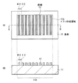
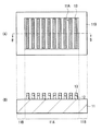
図1(A)は本技術の第1の実施の形態に係るエッチング方法を用いて形成された配線12のパターンの平面構成を表したものであり、図1(B)は図1(A)のB-B線に沿った断面構成を表している。この配線12は、基板11上の中央部のパターン形成領域11Aに、例えば幅W12が75nm、隣り合う配線12間の配線間隔I12が75nmで形成されている。配線12は、例えば表示装置および撮像装置等の電子デバイスの配線として利用されるものである。パターン形成領域11Aは、例えば表示装置および撮像装置等で複数の画素が配置された領域(画素部)に対応する。
<First Embodiment>
FIG. 1A shows a planar configuration of a pattern of the
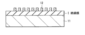
図2に示したように、配線12と基板11との間に絶縁膜Iが設けられていてもよい。この絶縁膜Iには例えばシリコン酸化膜(SiO2)等を用いることができる。基板11は例えば、石英,ガラス,シリコンまたはプラスチックフィルムなどの板状部材により構成されている。基板11の構成材料は、このエッチング方法を用いて製造する装置等の種類に応じて選択すればよい。配線12は、アルミニウム(Al),チタン(Ti),タンタル(Ta)およびタングステン(W)等の金属材料により構成されている。配線12は、積層構造を有するようにしてもよく、例えば、アルミニウムにチタン(Ti)および窒化チタン(TiN)を積層させるようにしてもよい(Ti/TiN/Al)。あるいは、タングステンシリサイド(WSi)をアルミニウムに積層させて(WSi/Al)配線12を構成するようにしてもよい。
As shown in FIG. 2, an insulating film I may be provided between the
このような配線12のパターンは、例えば、以下のようなエッチング方法を用いて形成する(図3〜図8)。なお、以下図3,4,6〜8では、図3(A),4(A),6(A),7(A),8(A)は上記図1(A)の平面構成に対応しており、図3(B),4(B),6(B),7(B),8(B)はそれぞれ図3(A),4(A),6(A),7(A),8(A)のB-B線に沿った断面構成を表している。
Such a pattern of the
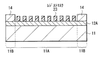
まず、基板11の全面に絶縁膜(図2の絶縁膜I)を設けた後、この絶縁膜上に例えばアルミニウムを含む金属膜12Aをスパッタリング法等のPVD(Physical Vapor Deposition)法により成膜する(図3(A),3(B))。次いで、図4(A),4(B)に示したように、基板11のパターン形成領域11Aには所定パターンのハードマスク13を設け、パターン形成領域11Aの周囲を囲むようにレジスト膜14を設ける(レジスト供給領域11B)。詳細は後述するが、本実施の形態では、このようなレジスト供給領域11Bを設けることにより、配線12が微細なパターンであっても、所望量の保護材(後述の図5の側壁保護膜14P)が生成され、配線12のサイドエッチングを抑えることが可能となる。レジスト供給領域11Bは、例えば表示装置および撮像装置等の画素部の外側に対応する部分である。
First, after an insulating film (insulating film I in FIG. 2) is provided on the entire surface of the
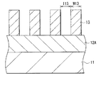
ハードマスク13およびレジスト供給領域11Bは、例えば以下のようにして形成する。まず、基板11の全面に例えばシリコン酸化膜を成膜した後、これにリソグラフィおよびドライエッチングによる加工を行い、パターン形成領域11Aにハードマスク13を形成する。シリコン酸化膜のパターニングには、例えばレジスト膜(図示せず)をパターニングして形成したマスクを用いる。次いで、例えばフォトリソグラフィ技術を用いて、このパターン形成領域11Aの周囲にレジスト膜14を形成する。これによりレジスト供給領域11Bが形成される。レジスト膜14には、例えば感光性の高分子材料を用いることができる。ハードマスク13には、上記シリコン酸化膜の他、例えばシリコン窒化膜(SiN)等を用いることも可能である。ハードマスク13の幅W13,間隔I13は、目的とする配線12(図1)の幅W12,配線間隔I12と例えば同じ値に設定する。ハードマスク13の幅W13を配線12の幅W12よりも大きくしてもよい。これにより、配線12のサイドエッチングを抑えることが可能となる。
The
ハードマスク13およびレジスト膜14を設けた後、ハードマスク13を用いて、金属膜12Aのドライエッチングを行う。ドライエッチングは、例えばプラズマによりエッチングガスをイオン化またはラジカル化して行う。エッチングガスには、例えば、Cl2またはBCl3等の塩素系ガスが用いられる。エッチングガスにメタン等の炭化水素系ガスを用いるようにしてもよい。このとき、レジスト膜14を構成する高分子材料が分解して炭素含有物が生成する。エッチングガスに炭化水素系ガスを用いた場合には、このエッチングガスからも炭素含有物が生成する。
After providing the
このような炭素含有物が、図5に示したように、側壁保護膜14Pとしてエッチング途中の金属膜12Aに付着し、基板11の表面に対して水平方向の過剰なエッチングを防止する。具体的には、金属膜12Aの厚み方向の側面がハードマスク13から露出されるので、この側面を側壁保護膜14Pが覆い、配線12(金属膜12A)のサイドエッチングが抑えられる。基板11と金属膜12Aとの間の絶縁膜I(図2)は、例えばエッチングストッパーとして機能する。
As shown in FIG. 5, such a carbon-containing material adheres to the
このように金属膜12Aをドライエッチング加工することにより、ハードマスク13で覆われた部分以外の金属膜12Aが除去され、パターン形成領域11Aには、ハードマスク13と同じパターンの配線12が形成される(図6)。次いで、レジスト供給領域11Bに残存した金属膜12Aを除去する。具体的には、図7に示したように、パターン形成領域11Aを例えばレジスト膜からなるマスク15で覆った後、このマスク15から露出された金属膜12Aをエッチングして除去する(図8)。このエッチングにはドライエッチングを用いてもよく、あるいはウェットエッチングを用いてもよい。レジスト供給領域11Bの金属膜12Aが、配線12およびその他の部品等に影響しない場合には、これを除去せずに残しておいてもよい。最後に、必要に応じてハードマスク13を除去することにより、図1に示した配線12が完成する。
By performing dry etching on the
このように、本実施の形態のエッチング方法では、パターン形成領域11Aの周囲にレジスト膜14を設けて、レジスト供給領域11Bを形成する。これにより、金属膜12Aをドライエッチングする際のサイドエッチングを防ぐことが可能となる。以下、これについて説明する。
Thus, in the etching method of the present embodiment, the resist
図9Aは比較例に係るエッチング方法の一工程の断面構成を表したものである。このエッチング方法では、レジスト供給領域を設けずに金属膜112Aのドライエッチングを行う。金属膜112A上には、レジスト膜からなる所定パターンのマスク114が設けられており、このマスク114の形状に対応して金属膜112Aのパターンが形成される。マスク114の幅W114は例えば100nmであり、このように精細なパターンを形成するためには、例えばKrF(248nm)またはArF(198nm)等を用いた露光を行う。このような露光工程に適用されるマスク114の厚みT114は薄く、例えばKrFでは厚みT114が300nm〜500nmのマスク114、ArFでは厚みT114が200nm〜300nmのマスク114がそれぞれ用いられる。このような薄いマスク114からは十分な量の側壁保護膜(図5の側壁保護膜14P)が供給できず、金属膜112Aのサイドエッチングが進行する。従って、金属膜112Aから形成される配線の幅W112は、その厚み方向において一定にならず、マスク114の幅W114よりも細くなる部分が形成される(W114>W112)。金属膜112Aが、例えばアルミニウム等の腐食しやすい材料から構成されている場合には、特に、サイドエッチングが生じ易い。
FIG. 9A shows a cross-sectional configuration of one step of the etching method according to the comparative example. In this etching method, the
金属膜112Aの膜厚が大きいと、レジスト膜からなるマスク114のみではエッチング選択性を確保することが困難な場合がある。金属膜112Aが積層構造を有する場合にも同様の問題が生じる虞がある。
If the thickness of the
このような場合には、図9Bに示したように、例えば酸化シリコン膜からなるハードマスク113を用いる。このハードマスク113を用いるエッチングでは、まず、金属膜112A上に酸化シリコン膜を成膜した後、この酸化シリコン膜上に所定パターンのレジスト膜(図示せず)を形成する。次いで、このレジスト膜をパターニングしてマスクを形成した後、このマスクを用いて酸化シリコン膜をドライエッチングで加工する。これにより、ハードマスク113が形成される。その後、このハードマスク113により金属膜112Aのドライエッチング加工を行う。このとき、ハードマスク113を形成するのに用いたレジスト膜から炭素含有物が生成するが、上記図9Aに示した方法よりも、存在するレジスト量が少ないので、よりサイドエッチングが進行し易い。従って、金属膜112Aから形成される配線の幅W112とハードマスク113の幅W113とは大きく異なる虞がある(W113>>W112)。
In such a case, as shown in FIG. 9B, for example, a
これに対し、本実施の形態のエッチング方法では、パターン形成領域11Aの周りにレジスト供給領域11Bが設けられているので、パターン形成領域11A内に存在するレジスト量が制限されても、レジスト供給領域11Bから側壁保護膜14P(図5)を補うことができる。よって、配線12の幅W12が微細であっても、配線12のサイドエッチングを防止することが可能となる。即ち、厚み方向における配線12の幅W12を一定にして、配線12の断面形状を矩形に近づけることができる。これにより、このエッチング方法を用いて形成した電子デバイスまたは偏光板等の特性を向上させることが可能となる。
On the other hand, in the etching method of the present embodiment, since the resist
また、パターン形成領域11Aに、ハードマスク13を用いることができるので、エッチング選択性を確保しつつ、配線12のサイドエッチングを防止することができる。
Further, since the
更に、パターン形成領域11Aの外側にレジスト供給領域11Bを形成するので、レジスト膜14が配線12(金属膜12A)のパターンに影響を及ぼす虞がない。
Furthermore, since the resist
このように、本実施の形態では、パターン形成領域11Aの周りにレジスト膜14を配置するようにしたので、金属膜12Aのドライエッチング工程でこのレジスト膜14から側壁保護膜14Pを生成させることができる。よって、配線12が微細なパターンであっても、十分な量の側壁保護膜14Pを供給し、配線12のサイドエッチングを抑えることが可能となる。
Thus, in this embodiment, since the resist
以下、上記実施の形態の変形例および他の実施の形態について説明するが、以降の説明において上記実施の形態と同一構成部分については同一符号を付してその説明は適宜省略する。 Hereinafter, modifications of the above-described embodiment and other embodiments will be described. In the following description, the same components as those of the above-described embodiment will be denoted by the same reference numerals, and the description thereof will be omitted as appropriate.
<変形例1>
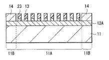
図10に示したように、金属膜12Aのパターニングにはハードマスク(図4のハードマスク13)に代えて、レジストマスク23を用いるようにしてもよい。あるいは、図11A,図11Bに示したように、ハードマスク13とレジストマスク23とを共に用いるようにしてもよい。基板11上に、レジストマスク23およびハードマスク13の順で形成してもよく(図11A)、基板11上にハードマスク13およびレジストマスク23の順に形成してもよい(図11B)。
<Modification 1>
As shown in FIG. 10, a resist
<第2の実施の形態>
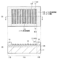
図12Aは、本技術の第2の実施の形態に係るエッチング方法の一工程を平面視で表したものである。このエッチング方法では、基板11上の複数の単位領域Pのうちの一部の単位領域Pにパターン形成領域11A、別の単位領域Pにレジスト供給領域11Bをそれぞれ形成する。この点を除き、このエッチング方法は上記第1の実施の形態と同様に行うものであり、その作用および効果も同様である。
<Second Embodiment>
FIG. 12A is a plan view illustrating one process of the etching method according to the second embodiment of the present technology. In this etching method, the
単位領域Pは、例えば表示装置の1パネルまたは半導体素子の1チップに相当する領域であり、基板11上にはこの単位領域P毎に複数のパターン形成領域11Aが形成される。なお、上述の図1は1の単位領域Pに相当する部分を表したものである。例えばパターン形成領域11Aの単位領域Pとレジスト供給領域11Bの単位領域Pとは交互に配置される(図12A)。パターン形成領域11Aおよびレジスト供給領域11Bの配置はどのようにしてもよく、例えばウェハ面内を均一にエッチングするために必要な側壁保護膜14P(図5)の量に応じて、レジスト供給領域11Bの単位領域Pの数を調整すればよい。
The unit region P is, for example, a region corresponding to one panel of a display device or one chip of a semiconductor element, and a plurality of
図12Bはパターン形成領域11Aが形成された単位領域Pの平面構成を表したものである。このように、この単位領域Pには金属膜12A上にハードマスク13が設けられ、金属膜12Aのドライエッチングがなされる。このパターン形成領域11Aが形成された単位領域Pの周囲のいずれかの単位領域Pは、レジスト供給領域11Bとなる。パターン形成領域11Aが形成された単位領域Pの周囲全部の単位領域Pがレジスト供給領域11Bであってもよい。
FIG. 12B shows a planar configuration of the unit region P in which the
図12Cは、レジスト供給領域11Bとなる単位領域Pの平面構成を表したものである。この単位領域Pでは、その全面にレジスト膜14が設けられている。即ち、図12Bに示したパターン形成領域11Aと同じ平面形状、同じ面積のレジスト膜14が設けられている。従って、金属膜12Aのドライエッチング加工を行う際に、1の単位領域P内にパターン形成領域11Aと共にレジスト供給領域11Bを設けた場合(例えば、図4)に比べて、より多くの側壁保護膜14Pを供給することが可能となる。よって、上記第1の実施の形態のエッチング方法に比べて、より確実に配線12のサイドエッチングを防ぐことが可能となる。また、パターン形成領域11Aが形成された単位領域Pとは別にレジスト供給領域11Bを形成するので、レジスト供給領域11Bに金属膜12Aが残存していても、パターン形成領域11Aに影響を及ぼす虞がない。よって、パターン形成領域11Aの金属膜12Aをパターニングした後に、レジスト供給領域11Bの金属膜12Aを除去する工程が不要となる。
FIG. 12C shows a planar configuration of the unit region P that becomes the resist
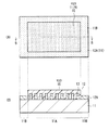
<変形例2>
図13に示したように、パターン形成領域11Aが形成された単位領域P内に、更に、レジスト供給領域11B(レジスト膜14)を設けるようにしてもよい。この単位領域Pでは、例えば上記第1の実施の形態で説明したのと同様に、中央部にパターン形成領域11Aが、その周囲にレジスト供給領域11Bがそれぞれ設けられている。これにより、単位領域Pの全面にレジスト膜14が設けられたレジスト供給領域11B(図12C)に加え、パターン形成領域11Aにより近い位置からも側壁保護膜14Pを供給して、サイドエッチングを防止することが可能となる。
<Modification 2>
As shown in FIG. 13, a resist
<第3の実施の形態>
図14Aは、本技術の第3の実施の形態に係るエッチング方法の一工程を平面視で表したものである。このエッチング方法では、基板11の中央部に各々パターン形成領域11Aが形成された複数の単位領域Pを設けて、この複数の単位領域Pの外側にレジスト供給領域11Bを形成する。この点を除き、このエッチング方法は上記第1,2の実施の形態と同様に行い、その作用および効果も同様である。
<Third Embodiment>
FIG. 14A is a plan view illustrating one process of the etching method according to the third embodiment of the present technology. In this etching method, a plurality of unit regions P each having a
図14Bはパターン形成領域11Aが形成された単位領域Pの平面構成を表したものである。この単位領域Pでは、金属膜12A上にハードマスク13が設けられ、金属膜12Aのドライエッチング加工がなされる。基板11上の全ての単位領域Pに、このようなパターン形成領域11Aが形成される。
FIG. 14B shows a planar configuration of the unit region P in which the
レジスト供給領域11B(レジスト膜14)は、この複数の単位領域P全体を囲むように形成される。金属膜12Aのドライエッチング加工を行う際には、このレジスト供給領域11Bから側壁保護膜14P(図5)が生成する。これにより、配線12のサイドエッチングが抑えられる。また、上記第2の実施の形態と同様に、パターン形成領域11Aが形成された単位領域Pの外側にレジスト供給領域11Bを形成するので、レジスト供給領域11Bの金属膜12を除去する工程が不要となる。
The resist
<変形例3>
図15に示したように、パターン形成領域11Aが形成された単位領域P内に、更に、レジスト供給領域11B(レジスト膜14)を設けるようにしてもよい。この単位領域Pでは、例えば上記第1の実施の形態で説明したのと同様に、中央部にパターン形成領域11Aが、その周囲にレジスト供給領域11Bがそれぞれ設けられている。これにより、単位領域Pの外側のレジスト供給領域11B(図14A)に加え、パターン形成領域11Aにより近い位置からも側壁保護膜14Pを供給してサイドエッチングを防止することが可能となる。
<Modification 3>
As shown in FIG. 15, a resist
<適用例>
上記本技術のエッチング方法は、例えばTFT(Thin Film Transistor)基板およびCMOS(Complementary Metal Oxide Semiconductor)基板等の配線基板の製造に適用可能である。配線基板の配線領域(パターン形成領域)に例えば上記本技術のエッチング方法により配線パターンが形成される。この配線基板を用いて、例えば表示装置および撮像装置等の電子デバイスが製造される。また、上記本技術のエッチング方法は、例えば偏光板の偏光パターンの形成に用いることも可能である。
<Application example>
The etching method of the present technology can be applied to the manufacture of wiring substrates such as TFT (Thin Film Transistor) substrates and CMOS (Complementary Metal Oxide Semiconductor) substrates. A wiring pattern is formed in the wiring region (pattern formation region) of the wiring substrate by, for example, the etching method of the present technology. Using this wiring board, for example, electronic devices such as a display device and an imaging device are manufactured. The etching method of the present technology can also be used for forming a polarizing pattern of a polarizing plate, for example.
図16は、本技術のエッチング方法を用いて製造した表示装置(表示装置1)の全体構成の一例を表したものである。表示装置1は、基板11と対向基板(図示せず)との間に例えば液晶層または有機EL(Electroluminescence)層等の表示層を含んでおり、この表示層が画素100毎に駆動されるようになっている。表示領域110には、画素100がマトリクス状に二次元配置されると共に画素100を駆動するための画素駆動回路140が設けられている。画素駆動回路140において、列方向(Y方向)には複数の信号線120A(120A1,120A2,・・・,120Am,・・・)が配置され、行方向(X方向)には複数の走査線130A(130A1,・・・,130An,・・・)が配置されている。信号線120Aと走査線130Aとの交差点に、一の画素100が設けられている。信号線120Aはその両端が信号線駆動回路120に接続され、走査線130Aはその両端が走査線駆動回路130に接続されている。
FIG. 16 illustrates an example of the entire configuration of a display device (display device 1) manufactured using the etching method of the present technology. The display device 1 includes a display layer such as a liquid crystal layer or an organic EL (Electroluminescence) layer between a
信号線駆動回路120は、信号供給源(図示せず)から供給される輝度情報に応じた映像信号の信号電圧を、信号線120Aを介して選択された画素100に供給するものである。走査線駆動回路130は、入力されるクロックパルスに同期してスタートパルスを順にシフト(転送)するシフトレジスタなどによって構成されている。走査線駆動回路130は、各画素100への映像信号の書き込みに際し行単位でそれらを走査し、各走査線130Aに走査信号を順次供給するものである。信号線120Aには信号線駆動回路120からの信号電圧が、走査線130Aには走査線駆動回路130からの走査信号がそれぞれ供給されるようになっている。例えば、このような画素駆動回路140の配線を上記本技術のエッチング方法を用いて形成することが可能である。
The signal
図17は、本技術のエッチング方法を用いて製造した固体撮像装置(撮像装置2)の全体構成を表している。この撮像装置2はCMOSイメージセンサであり、半導体基板11上の中央部に撮像エリアとしての画素部1aを有している。画素部1aの周辺領域には、例えば行走査部231、システム制御部232、水平選択部233および列走査部234を含む周辺回路部230が設けられている。
FIG. 17 illustrates an overall configuration of a solid-state imaging device (imaging device 2) manufactured using the etching method of the present technology. The imaging device 2 is a CMOS image sensor, and has a
画素部1aは、例えば行列状に2次元配置された複数の単位画素200を有している。この単位画素200には、例えば画素行ごとに画素駆動線Lread(具体的には行選択線およびリセット制御線)が、画素列ごとに垂直信号線Lsigが配線されている。画素駆動線Lreadは、画素からの信号読み出しのための駆動信号を伝送するものであり、その一端は行走査部231の各行に対応した出力端に接続されている。例えば、このような画素駆動線Lreadおよび垂直信号線Lsig等の配線を上記本技術のエッチング方法を用いて形成することが可能である。
The
<実施例>
以下、本技術の実施例について説明する。
<Example>
Hereinafter, examples of the present technology will be described.
(実験例1)
上記第2の実施の形態で説明したように、所定の単位領域にパターン形成領域、別の単位領域にレジスト供給領域をそれぞれ設け(図12A)、偏光板を作製した。このパターン形成領域が入光領域に相当する。具体的には、基板11上にアルミニウムからなる金属膜12Aを成膜した後、この金属膜12A上のパターン形成領域にハードマスク13を形成してドライエッチング加工を行った。基板11にはガラスを用いた。パターン形成領域を形成した単位領域の周囲の一部の単位領域全面にレジスト膜を設けて、レジスト供給領域を形成した。パターン形成領域のハードマスク13の幅W13を78nm、隣り合うハードマスク13間の間隔I13を72nmとした(図18)。
(Experimental example 1)
As described in the second embodiment, a pattern forming region is provided in a predetermined unit region, and a resist supply region is provided in another unit region (FIG. 12A), and a polarizing plate is manufactured. This pattern formation region corresponds to a light incident region. Specifically, after a
(実験例2)
レジスト供給領域を設けないことを除き、実験例1と同様にして偏光板を作製した(図9B)。ハードマスク13の幅W13を73nm、隣り合うハードマスク13間の間隔I13を77nmとした(図18)。
(Experimental example 2)
A polarizing plate was produced in the same manner as in Experimental Example 1 except that no resist supply region was provided (FIG. 9B). The width W13 of the
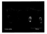
実験例1の偏光板のSEM写真を図19A、実験例2の偏光板のSEM写真を図19Bにそれぞれ示す。ドライエッチング後の金属膜(図1の配線12)の幅は、実験例1では59nm、実験例2では32nmであった。即ち、実験例1のサイドエッチング量は19nm、実験例2のサイドエッチング量は41nmであった。このように、レジスト供給領域を設けて作製した偏光板(実験例1)では、サイドエッチングを抑えることができた。
An SEM photograph of the polarizing plate of Experimental Example 1 is shown in FIG. 19A, and an SEM photograph of the polarizing plate of Experimental Example 2 is shown in FIG. 19B. The width of the metal film (
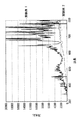
図20は実験例1,2の偏光板の消光比を表したものである。横軸が波長、縦軸が消光比をそれぞれ表している。実験例1の偏光板では、実験例2の偏光板に比べて消光比が大きく向上している。サイドエッチングを抑えて金属膜を所望の幅に精確にパターニングすることにより、偏光板の機能を高めることができることが確認された。 FIG. 20 shows the extinction ratio of the polarizing plates of Experimental Examples 1 and 2. The horizontal axis represents the wavelength, and the vertical axis represents the extinction ratio. In the polarizing plate of Experimental Example 1, the extinction ratio is greatly improved as compared with the polarizing plate of Experimental Example 2. It was confirmed that the function of the polarizing plate can be enhanced by accurately patterning the metal film to a desired width while suppressing side etching.
以上、実施の形態および変形例を挙げて本技術を説明したが、本技術はこれら実施の形態等に限定されず、種々の変形が可能である。例えば、上記実施の形態等において説明した各層の材料および厚み、または成膜方法および成膜条件などは限定されるものではなく、他の材料および厚みとしてもよく、または他の成膜方法および成膜条件としてもよい。 As described above, the present technology has been described with the embodiment and the modified examples, but the present technology is not limited to the embodiment and the like, and various modifications are possible. For example, the material and thickness of each layer described in the above embodiment and the like, or the film formation method and film formation conditions are not limited, and other materials and thicknesses may be used, or other film formation methods and film formation may be performed. It is good also as film | membrane conditions.
なお、本明細書に記載された効果はあくまで例示であって限定されるものではなく、また他の効果があってもよい。 In addition, the effect described in this specification is an illustration to the last, and is not limited, Moreover, there may exist another effect.
なお、本技術は以下のような構成を取ることも可能である。
(1)パターン形成領域を有する基板上に金属膜を成膜することと、前記パターン形成領域の金属膜上に所定パターンのマスクを形成すると共に、前記パターン形成領域の周囲の少なくとも一部にレジスト膜を成膜することと、前記パターン形成領域の金属膜をドライエッチングすることとを含むエッチング方法。
(2)前記ドライエッチングでは、前記金属膜の前記マスクから露出された面に前記レジスト膜から生成した側壁保護膜を付着させる前記(1)記載のエッチング方法。
(3)前記マスクとしてハードマスクを用いる前記(1)または(2)記載のエッチング方法。
(4)前記金属膜をアルミニウム,チタン,タンタルまたはタングステンを含む材料で成膜する前記(1)乃至(3)のうちいずれか1つに記載のエッチング方法。
(5)前記金属膜としてアルミニウム膜を含む積層膜を成膜する前記(1)乃至(4)のうちいずれか1つに記載のエッチング方法。
(6)前記マスクをレジスト材料により形成する前記(1)または(2)記載のエッチング方法。
(7)前記パターン形成領域を、前記基板に設けられた複数の単位領域各々に形成し、前記複数の単位領域の外側に前記レジスト膜を成膜する前記(1)乃至(6)のうちいずれか1つに記載のエッチング方法。
(8)前記パターン形成領域が形成された単位領域内に、更に前記レジスト膜を成膜する前記(7)記載のエッチング方法。
(9)前記パターン形成領域を前記基板に設けられた複数の単位領域のうちの一部の単位領域に形成すると共に、前記レジスト膜を別の単位領域に成膜する前記(1)乃至(8)のうちいずれか1つに記載のエッチング方法。
(10)前記パターン形成領域が形成された単位領域内に、更に前記レジスト膜を成膜する前記(9)記載のエッチング方法。
(11)配線形成領域を有する基板上に金属膜を成膜することと、前記配線形成領域の金属膜上に所定パターンのマスクを形成すると共に、前記配線形成領域の周囲の少なくとも一部にレジスト膜を成膜することと、前記配線形成領域の金属膜をドライエッチングすることにより配線パターンを形成することとを含む電子デバイスの製造方法。
(12)入光領域を有する基板上に金属膜を成膜することと、前記入光領域の金属膜上に所定パターンのマスクを形成すると共に、前記入光領域の周囲の少なくとも一部にレジスト膜を成膜することと、前記入光領域の金属膜をドライエッチングすることにより偏光パターンを形成することとを含む偏光板の製造方法。
In addition, this technique can also take the following structures.
(1) A metal film is formed on a substrate having a pattern formation region, a mask having a predetermined pattern is formed on the metal film in the pattern formation region, and a resist is formed on at least a part of the periphery of the pattern formation region. An etching method comprising: forming a film; and dry etching the metal film in the pattern formation region.
(2) The etching method according to (1), wherein in the dry etching, a sidewall protective film generated from the resist film is attached to a surface of the metal film exposed from the mask.
(3) The etching method according to (1) or (2), wherein a hard mask is used as the mask.
(4) The etching method according to any one of (1) to (3), wherein the metal film is formed of a material containing aluminum, titanium, tantalum, or tungsten.
(5) The etching method according to any one of (1) to (4), wherein a stacked film including an aluminum film is formed as the metal film.
(6) The etching method according to (1) or (2), wherein the mask is formed of a resist material.
(7) The pattern formation region is formed in each of a plurality of unit regions provided on the substrate, and the resist film is formed outside the plurality of unit regions, any of (1) to (6) The etching method as described in any one.
(8) The etching method according to (7), wherein the resist film is further formed in a unit region where the pattern formation region is formed.
(9) The pattern formation region is formed in a part of a plurality of unit regions provided on the substrate, and the resist film is formed in another unit region. The etching method according to any one of the above.
(10) The etching method according to (9), wherein the resist film is further formed in a unit region where the pattern formation region is formed.
(11) A metal film is formed on a substrate having a wiring formation region, a mask having a predetermined pattern is formed on the metal film in the wiring formation region, and a resist is formed on at least a part of the periphery of the wiring formation region. An electronic device manufacturing method comprising: forming a film; and forming a wiring pattern by dry etching the metal film in the wiring formation region.
(12) Forming a metal film on a substrate having a light incident region, forming a mask with a predetermined pattern on the metal film in the light incident region, and forming a resist on at least a part of the periphery of the light incident region A method for producing a polarizing plate, comprising: forming a film; and forming a polarization pattern by dry etching the metal film in the light incident region.
11・・・基板、11A・・・パターン形成領域、11B・・・レジスト供給領域、12・・・配線、12A・・・金属膜、I・・・絶縁膜、13・・・ハードマスク、14・・・レジスト膜、14P・・・側壁保護膜、15・・・マスク、23・・・レジストマスク、P・・・単位領域。
DESCRIPTION OF
Claims (12)
前記パターン形成領域の金属膜上に所定パターンのマスクを形成すると共に、前記パターン形成領域の周囲の少なくとも一部にレジスト膜を成膜することと、
前記パターン形成領域の金属膜をドライエッチングすることと
を含むエッチング方法。 Forming a metal film on a substrate having a pattern formation region;
Forming a mask having a predetermined pattern on the metal film in the pattern formation region, and forming a resist film on at least a part of the periphery of the pattern formation region;
Dry etching the metal film in the pattern formation region.
請求項1記載のエッチング方法。 The etching method according to claim 1, wherein in the dry etching, a sidewall protective film generated from the resist film is attached to a surface of the metal film exposed from the mask.
請求項1記載のエッチング方法。 The etching method according to claim 1, wherein a hard mask is used as the mask.
請求項1記載のエッチング方法。 The etching method according to claim 1, wherein the metal film is formed of a material containing aluminum, titanium, tantalum, or tungsten.
請求項1記載のエッチング方法。 The etching method according to claim 1, wherein a laminated film including an aluminum film is formed as the metal film.
請求項1記載のエッチング方法。 The etching method according to claim 1, wherein the mask is formed of a resist material.
前記複数の単位領域の外側に前記レジスト膜を成膜する
請求項1記載のエッチング方法。 Forming the pattern formation region in each of a plurality of unit regions provided on the substrate;
The etching method according to claim 1, wherein the resist film is formed outside the plurality of unit regions.
請求項7記載のエッチング方法。 The etching method according to claim 7, wherein the resist film is further formed in a unit region where the pattern formation region is formed.
請求項1記載のエッチング方法。 The etching method according to claim 1, wherein the pattern formation region is formed in a part of a plurality of unit regions provided on the substrate, and the resist film is formed in another unit region.
請求項9記載のエッチング方法。 The etching method according to claim 9, wherein the resist film is further formed in a unit region where the pattern formation region is formed.
前記配線形成領域の金属膜上に所定パターンのマスクを形成すると共に、前記配線形成領域の周囲の少なくとも一部にレジスト膜を成膜することと、
前記配線形成領域の金属膜をドライエッチングすることにより配線パターンを形成することと
を含む電子デバイスの製造方法。 Forming a metal film on a substrate having a wiring formation region;
Forming a mask having a predetermined pattern on the metal film in the wiring formation region, and forming a resist film on at least a part of the periphery of the wiring formation region;
Forming a wiring pattern by dry etching the metal film in the wiring forming region.
前記入光領域の金属膜上に所定パターンのマスクを形成すると共に、前記入光領域の周囲の少なくとも一部にレジスト膜を成膜することと、
前記入光領域の金属膜をドライエッチングすることにより偏光パターンを形成することと
を含む偏光板の製造方法。 Forming a metal film on a substrate having a light incident region;
Forming a mask having a predetermined pattern on the metal film in the light incident region, and forming a resist film on at least a part of the periphery of the light incident region;
Forming a polarization pattern by dry-etching the metal film in the light incident region.
Priority Applications (2)
| Application Number | Priority Date | Filing Date | Title |
|---|---|---|---|
| JP2013176347A JP2015046459A (en) | 2013-08-28 | 2013-08-28 | Etching method, method of manufacturing electronic device, and method of manufacturing polarizing device |
| US14/456,944 US9316771B2 (en) | 2013-08-28 | 2014-08-11 | Etching process, method of manufacturing electronic device, and method of manufacturing polarizing plate |
Applications Claiming Priority (1)
| Application Number | Priority Date | Filing Date | Title |
|---|---|---|---|
| JP2013176347A JP2015046459A (en) | 2013-08-28 | 2013-08-28 | Etching method, method of manufacturing electronic device, and method of manufacturing polarizing device |
Publications (2)
| Publication Number | Publication Date |
|---|---|
| JP2015046459A true JP2015046459A (en) | 2015-03-12 |
| JP2015046459A5 JP2015046459A5 (en) | 2016-03-03 |
Family
ID=52581678
Family Applications (1)
| Application Number | Title | Priority Date | Filing Date |
|---|---|---|---|
| JP2013176347A Pending JP2015046459A (en) | 2013-08-28 | 2013-08-28 | Etching method, method of manufacturing electronic device, and method of manufacturing polarizing device |
Country Status (2)
| Country | Link |
|---|---|
| US (1) | US9316771B2 (en) |
| JP (1) | JP2015046459A (en) |
Cited By (2)
| Publication number | Priority date | Publication date | Assignee | Title |
|---|---|---|---|---|
| KR20160120814A (en) * | 2015-04-08 | 2016-10-19 | 삼성디스플레이 주식회사 | Wire grid polarizer and method for fabricating the same |
| JP2018189982A (en) * | 2018-07-26 | 2018-11-29 | デクセリアルズ株式会社 | Polarizing plate and optical instrument |
Families Citing this family (1)
| Publication number | Priority date | Publication date | Assignee | Title |
|---|---|---|---|---|
| JP2019061125A (en) * | 2017-09-27 | 2019-04-18 | デクセリアルズ株式会社 | Polarizer, manufacturing method for the same and optical equipment |
Citations (7)
| Publication number | Priority date | Publication date | Assignee | Title |
|---|---|---|---|---|
| JPS6289331A (en) * | 1985-10-16 | 1987-04-23 | Toshiba Corp | Processing fine pattern |
| JPH02228020A (en) * | 1989-02-28 | 1990-09-11 | Rohm Co Ltd | Manufacture of integrated circuit |
| JPH07230986A (en) * | 1994-02-18 | 1995-08-29 | Sony Corp | Etching method |
| JP2000058507A (en) * | 1998-08-17 | 2000-02-25 | Sony Corp | Manufacture of semiconductor device |
| JP2006310634A (en) * | 2005-04-28 | 2006-11-09 | Sharp Corp | Method for manufacturing semiconductor device |
| JP2012103469A (en) * | 2010-11-10 | 2012-05-31 | Asahi Kasei Corp | Optical element and projection type liquid crystal display device |
| WO2013190681A1 (en) * | 2012-06-21 | 2013-12-27 | 日立コンシューマエレクトロニクス株式会社 | Optical element, production method for optical element, and optical device |
Family Cites Families (5)
| Publication number | Priority date | Publication date | Assignee | Title |
|---|---|---|---|---|
| DE3175019D1 (en) * | 1980-04-02 | 1986-09-04 | Hitachi Ltd | Method of forming patterns |
| TW448503B (en) * | 1999-03-11 | 2001-08-01 | Toshiba Corp | Method for dry etching |
| JP2009188224A (en) | 2008-02-07 | 2009-08-20 | Seiko Instruments Inc | Semiconductor device manufacturing method |
| JP5182061B2 (en) * | 2008-12-17 | 2013-04-10 | セイコーエプソン株式会社 | Polarizing element and manufacturing method of polarizing element, liquid crystal device, electronic device, and projection display device |
| JP5427104B2 (en) * | 2010-05-11 | 2014-02-26 | パナソニック株式会社 | Pattern formation method |
-
2013
- 2013-08-28 JP JP2013176347A patent/JP2015046459A/en active Pending
-
2014
- 2014-08-11 US US14/456,944 patent/US9316771B2/en active Active
Patent Citations (7)
| Publication number | Priority date | Publication date | Assignee | Title |
|---|---|---|---|---|
| JPS6289331A (en) * | 1985-10-16 | 1987-04-23 | Toshiba Corp | Processing fine pattern |
| JPH02228020A (en) * | 1989-02-28 | 1990-09-11 | Rohm Co Ltd | Manufacture of integrated circuit |
| JPH07230986A (en) * | 1994-02-18 | 1995-08-29 | Sony Corp | Etching method |
| JP2000058507A (en) * | 1998-08-17 | 2000-02-25 | Sony Corp | Manufacture of semiconductor device |
| JP2006310634A (en) * | 2005-04-28 | 2006-11-09 | Sharp Corp | Method for manufacturing semiconductor device |
| JP2012103469A (en) * | 2010-11-10 | 2012-05-31 | Asahi Kasei Corp | Optical element and projection type liquid crystal display device |
| WO2013190681A1 (en) * | 2012-06-21 | 2013-12-27 | 日立コンシューマエレクトロニクス株式会社 | Optical element, production method for optical element, and optical device |
Cited By (8)
| Publication number | Priority date | Publication date | Assignee | Title |
|---|---|---|---|---|
| KR20160120814A (en) * | 2015-04-08 | 2016-10-19 | 삼성디스플레이 주식회사 | Wire grid polarizer and method for fabricating the same |
| KR102413970B1 (en) * | 2015-04-08 | 2022-06-28 | 삼성디스플레이 주식회사 | Wire grid polarizer and method for fabricating the same |
| JP2018189982A (en) * | 2018-07-26 | 2018-11-29 | デクセリアルズ株式会社 | Polarizing plate and optical instrument |
| WO2020022433A1 (en) * | 2018-07-26 | 2020-01-30 | デクセリアルズ株式会社 | Polarizer and optical equipment |
| CN110998383A (en) * | 2018-07-26 | 2020-04-10 | 迪睿合株式会社 | Polarizing plate and optical device |
| CN110998383B (en) * | 2018-07-26 | 2022-03-22 | 迪睿合株式会社 | Polarizing plate and optical device |
| US11500140B2 (en) | 2018-07-26 | 2022-11-15 | Dexerials Corporation | Polarizing plate and optical apparatus having tip portions with continuous curved surface |
| JP7226936B2 (en) | 2018-07-26 | 2023-02-21 | デクセリアルズ株式会社 | Polarizing plate and optical equipment |
Also Published As
| Publication number | Publication date |
|---|---|
| US20150060396A1 (en) | 2015-03-05 |
| US9316771B2 (en) | 2016-04-19 |
Similar Documents
| Publication | Publication Date | Title |
|---|---|---|
| JP5044273B2 (en) | Thin film transistor array substrate, manufacturing method thereof, and display device | |
| JP6129206B2 (en) | Manufacturing method of TFT array substrate | |
| KR100937173B1 (en) | An Array Substrate of Thin Film Transistor Liquid Crystal Display Device and the method for fabricating thereof | |
| US20170090233A1 (en) | Display Substrate, Method of Fabricating the Same, and Display Device | |
| WO2016078272A1 (en) | Substrate and manufacturing method thereof, and display device | |
| JP4519759B2 (en) | TFT-LCD array substrate and manufacturing method thereof | |
| JP4872591B2 (en) | TFT substrate, manufacturing method thereof, and display device including the TFT substrate | |
| JP7079548B2 (en) | Manufacturing method of array board, display device and array board | |
| JP2010283326A (en) | Array substrate and method of manufacturing the same | |
| US7335538B2 (en) | Method for manufacturing bottom substrate of liquid crystal display device | |
| JP2009206306A (en) | Method for manufacturing semiconductor apparatus, and method of manufacturing electro-optical apparatus | |
| WO2015096312A1 (en) | Array substrate and manufacturing method thereof, and display device | |
| JP2008053517A (en) | Array substrate and method of manufacturing the same | |
| JP5063936B2 (en) | Manufacturing method of TFT array substrate | |
| US8575031B2 (en) | Method of forming a fine pattern, display substrate, and method of manufacturing the same using the method of forming a fine pattern | |
| JP2015046459A (en) | Etching method, method of manufacturing electronic device, and method of manufacturing polarizing device | |
| WO2013071838A1 (en) | Color film substrate, tft array substrate, manufacturing method thereof and liquid crystal display panel | |
| JP2006295121A (en) | Liquid crystal display device using thin film transistor, and its manufacturing device | |
| KR20110125399A (en) | Method of manufacturing thin film transistor and method of manufacturing flat panel display device using the same | |
| JP2010192611A (en) | Method of manufacturing semiconductor device substrate, and semiconductor device substrate | |
| US20030203627A1 (en) | Method for fabricating thin film transistor | |
| JP6006889B2 (en) | Active matrix substrate manufacturing method, active matrix substrate, and display device | |
| JP4480442B2 (en) | Manufacturing method of liquid crystal display device | |
| JP5707725B2 (en) | Thin film patterning method and display panel manufacturing method | |
| JP2011222688A5 (en) |
Legal Events
| Date | Code | Title | Description |
|---|---|---|---|
| A521 | Request for written amendment filed |
Free format text: JAPANESE INTERMEDIATE CODE: A523 Effective date: 20160119 |
|
| A621 | Written request for application examination |
Free format text: JAPANESE INTERMEDIATE CODE: A621 Effective date: 20160119 |
|
| A977 | Report on retrieval |
Free format text: JAPANESE INTERMEDIATE CODE: A971007 Effective date: 20161124 |
|
| A131 | Notification of reasons for refusal |
Free format text: JAPANESE INTERMEDIATE CODE: A131 Effective date: 20161206 |
|
| A521 | Request for written amendment filed |
Free format text: JAPANESE INTERMEDIATE CODE: A523 Effective date: 20170119 |
|
| A131 | Notification of reasons for refusal |
Free format text: JAPANESE INTERMEDIATE CODE: A131 Effective date: 20170523 |
|
| A02 | Decision of refusal |
Free format text: JAPANESE INTERMEDIATE CODE: A02 Effective date: 20170718 |