EP1033810A2 - A method of manufacturing a surface acoustic wave apparatus - Google Patents
A method of manufacturing a surface acoustic wave apparatus Download PDFInfo
- Publication number
- EP1033810A2 EP1033810A2 EP00400562A EP00400562A EP1033810A2 EP 1033810 A2 EP1033810 A2 EP 1033810A2 EP 00400562 A EP00400562 A EP 00400562A EP 00400562 A EP00400562 A EP 00400562A EP 1033810 A2 EP1033810 A2 EP 1033810A2
- Authority
- EP
- European Patent Office
- Prior art keywords
- acoustic wave
- surface acoustic
- manufacturing
- base member
- wave apparatus
- Prior art date
- Legal status (The legal status is an assumption and is not a legal conclusion. Google has not performed a legal analysis and makes no representation as to the accuracy of the status listed.)
- Granted
Links
Images
Classifications
-
- H—ELECTRICITY
- H03—ELECTRONIC CIRCUITRY
- H03H—IMPEDANCE NETWORKS, e.g. RESONANT CIRCUITS; RESONATORS
- H03H9/00—Networks comprising electromechanical or electro-acoustic elements; Electromechanical resonators
- H03H9/02—Details
- H03H9/05—Holders or supports
- H03H9/10—Mounting in enclosures
- H03H9/1064—Mounting in enclosures for surface acoustic wave [SAW] devices
- H03H9/1071—Mounting in enclosures for surface acoustic wave [SAW] devices the enclosure being defined by a frame built on a substrate and a cap, the frame having no mechanical contact with the SAW device
-
- H—ELECTRICITY
- H03—ELECTRONIC CIRCUITRY
- H03H—IMPEDANCE NETWORKS, e.g. RESONANT CIRCUITS; RESONATORS
- H03H3/00—Apparatus or processes specially adapted for the manufacture of impedance networks, resonating circuits, resonators
- H03H3/007—Apparatus or processes specially adapted for the manufacture of impedance networks, resonating circuits, resonators for the manufacture of electromechanical resonators or networks
- H03H3/08—Apparatus or processes specially adapted for the manufacture of impedance networks, resonating circuits, resonators for the manufacture of electromechanical resonators or networks for the manufacture of resonators or networks using surface acoustic waves
-
- H—ELECTRICITY
- H03—ELECTRONIC CIRCUITRY
- H03H—IMPEDANCE NETWORKS, e.g. RESONANT CIRCUITS; RESONATORS
- H03H9/00—Networks comprising electromechanical or electro-acoustic elements; Electromechanical resonators
- H03H9/02—Details
- H03H9/02535—Details of surface acoustic wave devices
- H03H9/02818—Means for compensation or elimination of undesirable effects
- H03H9/02929—Means for compensation or elimination of undesirable effects of ageing changes of characteristics, e.g. electro-acousto-migration
-
- H—ELECTRICITY
- H03—ELECTRONIC CIRCUITRY
- H03H—IMPEDANCE NETWORKS, e.g. RESONANT CIRCUITS; RESONATORS
- H03H9/00—Networks comprising electromechanical or electro-acoustic elements; Electromechanical resonators
- H03H9/02—Details
- H03H9/05—Holders or supports
- H03H9/058—Holders or supports for surface acoustic wave devices
- H03H9/059—Holders or supports for surface acoustic wave devices consisting of mounting pads or bumps
-
- H—ELECTRICITY
- H03—ELECTRONIC CIRCUITRY
- H03H—IMPEDANCE NETWORKS, e.g. RESONANT CIRCUITS; RESONATORS
- H03H9/00—Networks comprising electromechanical or electro-acoustic elements; Electromechanical resonators
- H03H9/25—Constructional features of resonators using surface acoustic waves
-
- H—ELECTRICITY
- H03—ELECTRONIC CIRCUITRY
- H03H—IMPEDANCE NETWORKS, e.g. RESONANT CIRCUITS; RESONATORS
- H03H9/00—Networks comprising electromechanical or electro-acoustic elements; Electromechanical resonators
- H03H9/46—Filters
- H03H9/64—Filters using surface acoustic waves
-
- H—ELECTRICITY
- H03—ELECTRONIC CIRCUITRY
- H03H—IMPEDANCE NETWORKS, e.g. RESONANT CIRCUITS; RESONATORS
- H03H9/00—Networks comprising electromechanical or electro-acoustic elements; Electromechanical resonators
- H03H9/02—Details
- H03H9/02535—Details of surface acoustic wave devices
- H03H9/02543—Characteristics of substrate, e.g. cutting angles
- H03H9/02574—Characteristics of substrate, e.g. cutting angles of combined substrates, multilayered substrates, piezoelectrical layers on not-piezoelectrical substrate
-
- H—ELECTRICITY
- H10—SEMICONDUCTOR DEVICES; ELECTRIC SOLID-STATE DEVICES NOT OTHERWISE PROVIDED FOR
- H10W—GENERIC PACKAGES, INTERCONNECTIONS, CONNECTORS OR OTHER CONSTRUCTIONAL DETAILS OF DEVICES COVERED BY CLASS H10
- H10W90/00—Package configurations
- H10W90/701—Package configurations characterised by the relative positions of pads or connectors relative to package parts
- H10W90/721—Package configurations characterised by the relative positions of pads or connectors relative to package parts of bump connectors
- H10W90/724—Package configurations characterised by the relative positions of pads or connectors relative to package parts of bump connectors between a chip and a stacked insulating package substrate, interposer or RDL
-
- Y—GENERAL TAGGING OF NEW TECHNOLOGICAL DEVELOPMENTS; GENERAL TAGGING OF CROSS-SECTIONAL TECHNOLOGIES SPANNING OVER SEVERAL SECTIONS OF THE IPC; TECHNICAL SUBJECTS COVERED BY FORMER USPC CROSS-REFERENCE ART COLLECTIONS [XRACs] AND DIGESTS
- Y10—TECHNICAL SUBJECTS COVERED BY FORMER USPC
- Y10T—TECHNICAL SUBJECTS COVERED BY FORMER US CLASSIFICATION
- Y10T29/00—Metal working
- Y10T29/42—Piezoelectric device making
-
- Y—GENERAL TAGGING OF NEW TECHNOLOGICAL DEVELOPMENTS; GENERAL TAGGING OF CROSS-SECTIONAL TECHNOLOGIES SPANNING OVER SEVERAL SECTIONS OF THE IPC; TECHNICAL SUBJECTS COVERED BY FORMER USPC CROSS-REFERENCE ART COLLECTIONS [XRACs] AND DIGESTS
- Y10—TECHNICAL SUBJECTS COVERED BY FORMER USPC
- Y10T—TECHNICAL SUBJECTS COVERED BY FORMER US CLASSIFICATION
- Y10T29/00—Metal working
- Y10T29/49—Method of mechanical manufacture
- Y10T29/49002—Electrical device making
- Y10T29/49004—Electrical device making including measuring or testing of device or component part
-
- Y—GENERAL TAGGING OF NEW TECHNOLOGICAL DEVELOPMENTS; GENERAL TAGGING OF CROSS-SECTIONAL TECHNOLOGIES SPANNING OVER SEVERAL SECTIONS OF THE IPC; TECHNICAL SUBJECTS COVERED BY FORMER USPC CROSS-REFERENCE ART COLLECTIONS [XRACs] AND DIGESTS
- Y10—TECHNICAL SUBJECTS COVERED BY FORMER USPC
- Y10T—TECHNICAL SUBJECTS COVERED BY FORMER US CLASSIFICATION
- Y10T29/00—Metal working
- Y10T29/49—Method of mechanical manufacture
- Y10T29/49002—Electrical device making
- Y10T29/49005—Acoustic transducer
-
- Y—GENERAL TAGGING OF NEW TECHNOLOGICAL DEVELOPMENTS; GENERAL TAGGING OF CROSS-SECTIONAL TECHNOLOGIES SPANNING OVER SEVERAL SECTIONS OF THE IPC; TECHNICAL SUBJECTS COVERED BY FORMER USPC CROSS-REFERENCE ART COLLECTIONS [XRACs] AND DIGESTS
- Y10—TECHNICAL SUBJECTS COVERED BY FORMER USPC
- Y10T—TECHNICAL SUBJECTS COVERED BY FORMER US CLASSIFICATION
- Y10T29/00—Metal working
- Y10T29/49—Method of mechanical manufacture
- Y10T29/49002—Electrical device making
- Y10T29/49117—Conductor or circuit manufacturing
- Y10T29/49124—On flat or curved insulated base, e.g., printed circuit, etc.
- Y10T29/4913—Assembling to base an electrical component, e.g., capacitor, etc.
-
- Y—GENERAL TAGGING OF NEW TECHNOLOGICAL DEVELOPMENTS; GENERAL TAGGING OF CROSS-SECTIONAL TECHNOLOGIES SPANNING OVER SEVERAL SECTIONS OF THE IPC; TECHNICAL SUBJECTS COVERED BY FORMER USPC CROSS-REFERENCE ART COLLECTIONS [XRACs] AND DIGESTS
- Y10—TECHNICAL SUBJECTS COVERED BY FORMER USPC
- Y10T—TECHNICAL SUBJECTS COVERED BY FORMER US CLASSIFICATION
- Y10T29/00—Metal working
- Y10T29/49—Method of mechanical manufacture
- Y10T29/49002—Electrical device making
- Y10T29/49117—Conductor or circuit manufacturing
- Y10T29/49124—On flat or curved insulated base, e.g., printed circuit, etc.
- Y10T29/49147—Assembling terminal to base
- Y10T29/49149—Assembling terminal to base by metal fusion bonding
Definitions
- the present invention relates to a method of manufacturing a surface acoustic wave apparatus in which a surface acoustic wave element is sealed in a package.
- a surface acoustic wave apparatus is formed by connecting and fixing a surface acoustic wave element onto a base member through bump bonding, then by sealing the surface acoustic wave element in a package defined by bonding a cap member onto the base member.
- a seam welding method has been used and a Kovar alloy is used to define a joint so as to form an air-tight fixation between the base member and the cap member.
- sealing methods other than the seam welding method include a wax sealing method which requires that a wax material is applied to connecting portions of either the base member or the cap member, a small heater block is then contacted with for example the cap member, thereby heating the cap member so as to melt the wax material, followed by a cooling treatment to join the base member with the cap member.
- the connecting portion of either the cap member or the base member is only partially heated so as to be elevated to a high temperature, resulting in the base member and the cap member being joined together under a condition involving a significant temperature difference between the connecting portions and other portions. Then, with the cooling of the surface acoustic wave apparatus, a large residual stress is generated between the base member and the cap member, hence causing the base member 10 and the cap member 30 to deform significantly, as shown in Fig. 3.
- metal bumps 51 which have been used to connect and fix the surface acoustic wave element 20 on to the base member 10, and is also concentrated on electrodes 12 and 25 combined with metal bumps 51. Accordingly, there had been a problem that the metal bumps 51 and the electrodes 12, 25 would be damaged and are caused to peel off, resulting in some defective connections and defective characteristics.
- preferred embodiments of the present invention provide a method of manufacturing a surface acoustic wave apparatus which reduces and minimizes a stress exerted on the metal bumps during a process of joining the base member and the cap member, and prevents problems occurring in connecting portions of the metal bumps, thereby ensuring a sufficient reliability.
- a preferred embodiment of the method of manufacturing a surface acoustic wave apparatus includes the steps of bump-bonding a surface acoustic wave element and a base member together through metal bumps having a melting point of about 450°C or higher such that the surface acoustic wave apparatus is fixed in a face down configuration to a bottom surface of a recess of the base member; and bonding a cap member and the base member with a wax material by heating the cap member and the base member uniformly at a temperature higher than a melting point of the wax material to melt the wax material.
- the surface acoustic wave element may be bump bonded or joined in advance by way of metal bumps having a melting point of about 450°C or higher, so as to be strongly supported and fixed on the base member while at the same time being electrically connected.
- the wax material it is preferable to use a solder, an Au-Sn alloy, or a low melting point glass which has a softening point of not more than about 450°C.
- the surface acoustic wave element is strongly connected and fixed on the base member via metal bumps having a melting point of about 450°C or higher and the surface acoustic wave apparatus as a whole is uniformly heated so as to join the base member with the cap member, thereby greatly reducing a stress exerted on the metal bump connecting portions. Therefore, it is possible to prevent the connection problems occurring in the metal bumps and the bump connecting portions, thereby obtaining a surface acoustic wave apparatus having a high reliability.
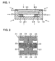
- Fig. 1 is a cross sectional view of a surface acoustic wave apparatus made according to a preferred embodiment of the present invention.
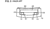
- Fig. 2 is a plan view indicating a surface acoustic wave element made according to a preferred embodiment.
- Fig. 3 is a brief cross sectional view for explaining a deformation occurring during a process when the base member and the cap member are joined together to form a conventional surface acoustic wave apparatus.
- Fig. 1 is a cross sectional view illustrating a surface acoustic wave apparatus manufactured according to a preferred embodiment of the present invention
- Fig. 2 is a plan view illustrating a surface acoustic wave element shown in Fig. 1.
- a plurality of electrode pads 25 of the surface acoustic wave element 20 and a plurality of electrode lands 12 formed on the surface of a recess portion of a base member 10 are bump bonded through metal bumps 51 with a face-down configuration.
- the surface acoustic wave element 20 is fixed and supported on the base member 10 and is electrically connected thereon.
- a cap member 30 is joined with the base member 10 via a wax material 52 having a high melting point wax such that the surface acoustic wave element 20 is covered up.
- the surface acoustic wave element 20 may be air-tightly sealed in the package (within the space) defined by the base member 10 and the cap member 30.
- a gap (a space) is provided for more efficiently propagating the surface acoustic wave, as shown in Fig. 1.
- the surface acoustic wave element 20 includes, as shown in Fig. 2, a piezoelectric substrate 21.
- a piezoelectric substrate 21 On the upper surface of the piezoelectric substrate 21, there is an electrode pattern including IDT (interdigital transducer) electrodes 22, reflector electrodes 23, outlet electrodes 24 extending from all of the IDT electrodes 22, and electrode pads 25 connected with all of the outlet electrodes 24.
- the electrode pattern is preferably made of A1 or it may be made of an alloy containing A1, and is preferably formed by using a known film formation method.
- the base member 10 preferably has a concave configuration and is formed preferably by laminating a plurality of ceramic layers, and has an input/output electrode pattern and an earth electrode pattern including a plurality of electrode lands 12 extending on its underside surface, the inner surface of its recess portion and inside itself.
- input and output terminal electrodes are provided on the underside surface of the base member 10.
- the surface acoustic wave apparatus may be mounted on a mounting board (a circuit board).
- the cap member 30 is preferably a metal plate made of a Fe-Ni alloy or an alloy containing Fe, or other suitable material, and may be subjected to a plating treatment if necessary.
- the surface acoustic wave apparatus is preferably manufactured in the following way.
- a ball-bonding method is preferably used to form a metal bump 51 on each electrode pad 25 of the surface acoustic wave element 20, with the each metal bump 51 preferably made of Au or a material containing Au as its main component.
- the surface acoustic wave element 20 is arranged face down such that its surface acoustic wave propagating surface including IDTs and other electrodes is caused to face toward the base member 10, followed by the simultaneous application of a supersonic wave and heat.
- each electrode pad 25 and its corresponding electrode land 12 of the base member 10 are joined together through a metal bump 51, thereby connecting and the fixing the surface acoustic wave element 20 on the base member 10.
- each metal bump 51 of Au it is not necessary to form each metal bump 51 of Au, and it is possible to form the metal bump 51 of other metal materials, provided that such metal materials do not easily become molten or softened during a subsequent process for joining together the base member 10 and the cap member 30 and that such materials preferably have a melting point of about 450°C or higher.
- a method of forming the metal bumps is not necessarily limited to the ball-bonding method. It is also possible to use other methods for forming the metal bumps, such as a bump formation method involving a plating treatment.
- the cap member 30 on which a wax for forming the wax material 52 and having a high melting point is mounted so as to press on the cap member, is laid over the base member 10.
- the cap member 30 and the base member 10 are introduced into a reflow furnace so that the base member 10, the surface acoustic wave element 20 and the cap member 30 are all uniformly heated, to a temperature higher than the melting point of the wax material 52, as indicated by arrows in Fig. 1, thereby melting the wax material 52 and thus causing the base member 10 and the cap member 30 to be joined together.
- the temperature for heat is preferably not more than about 450°C so that the bump does not melt.
- the base member and the cap member are joined together in a process where the surface acoustic wave apparatus as a whole is uniformly heated, there will be no temperature difference between the different members during the joining treatment. Therefore, a residual stress exerted on the surface acoustic wave apparatus after cooling treatment is minimized to be extremely small, thus greatly reducing the stress on the metal bump connecting portions.
- wax material apart from the above-described wax, it is also possible to use an Au-Sn alloy or a low melting point glass. Further, although it has been described in the above preferred embodiment that the wax material was mounted on the cap member pressing the same, it is also possible that the wax material may be formed in advance on the base member, or alternatively it may be formed through printing treatment.
- a reflow furnace may be used to join together the base member and the cap member, the present invention is not so limited. It is also possible to use a heating furnace or an oven capable of uniformly heating the entire surface acoustic wave apparatus.
- a material forming the cap member should not be limited to the Fe-Ni alloy or an alloy containing Fe. It is also possible to use other material capable of achieving an excellent airtight sealing property when used with the wax material. Further, a material for forming the cap member should not be limited to a metal. It is also possible to use a ceramic material to form the cap member. In such a case, it is possible to use a low melting point glass as a wax material. In addition, it is possible to use a base member formed of a metal.
- the shapes of the base member and the cap member should not be limited to that in the above described preferred embodiment. It is also possible, for example, to make a package defined by a flat plate like base member and a concave cap member. Moreover, the electrode pattern of the surface acoustic wave element should not be limited to that of the above preferred embodiment.
Landscapes
- Physics & Mathematics (AREA)
- Acoustics & Sound (AREA)
- Engineering & Computer Science (AREA)
- Manufacturing & Machinery (AREA)
- Surface Acoustic Wave Elements And Circuit Networks Thereof (AREA)
Abstract
Description
Claims (20)
- A method of manufacturing a surface acoustic wave apparatus, comprising the steps of:bump-bonding a surface acoustic wave element (20) and a base member (10) together through bumps (51) having a melting point of about 450°C or higher such that the surface acoustic wave element (20) is fixed with a face down configuration to a bottom surface of a recess of the base member (10); andbonding a cap member (30) and the base member (10) with a wax material (52) by heating the cap member (30) and the base member (10) substantially uniformly at a temperature higher than a melting point of the wax material to melt the wax material.
- The method of manufacturing a surface acoustic wave apparatus according to claim 1, wherein the wax material is selected from the group consisting of a solder, an Au-Sn alloy and a low melting point glass.
- The method of manufacturing a surface acoustic wave apparatus according to claim 1 or 2, wherein a plurality of electrode pads (25) are provided on the surface acoustic wave element (20) and a plurality of electrode lands (12) are provided on the surface of the recess of the base member (10), and the bumps (51) connect the electrode pads (25) and the electrode lands (12).
- The method of manufacturing a surface acoustic wave apparatus according to claim 1, 2 or 3, wherein the bumps (51) used during the bump bonding process are made of metal.
- The method of manufacturing a surface acoustic wave apparatus according to any previous claim, wherein the surface acoustic wave element (20) is sealed in an air-tight manner in the package defined by the base member (10) and the cap member (30).
- The method of manufacturing a surface acoustic wave apparatus according to any previous claim, wherein a gap is defined between the surface acoustic wave element (20) and the base member (10).
- The method of manufacturing a surface acoustic wave apparatus according to any previous claim, wherein the surface acoustic wave element (20) includes a piezoelectric substrate (21) and interdigital transducer electrodes (22), reflector electrodes (23), outlet electrodes (24) extending from the interdigital transducer electrodes, and electrode pads (25) connected with the outlet electrodes.
- The method of manufacturing a surface acoustic wave apparatus according to claim 7, wherein the piezoelectric substrate (21) is made of one of lithium tantalate and lithium niobate.
- The method of manufacturing a surface acoustic wave apparatus according to claim 7 or 8, wherein the electrode pattern is of one of A1 and an alloy containing A1.
- The method of manufacturing a surface acoustic wave apparatus according to any previous claims, wherein the base member (10) has a concave configuration.
- The method of manufacturing a surface acoustic wave apparatus according to any previous claim, wherein the base member (10) is formed by laminating a plurality of ceramic layers.
- The method of manufacturing a surface acoustic wave apparatus according to any previous claim, wherein the cap member (30) includes a metal plate made of one of a Fe-Ni alloy and an alloy containing Fe.
- The method of manufacturing a surface acoustic wave apparatus according to any previous claim, further including the step of simultaneously applying a supersonic wave and heat so that the surface acoustic wave element (20) is fixed with a face down configuration to the bottom surface of the recess of the base member (10).
- The method of manufacturing a surface acoustic wave apparatus according to claim 13, wherein a plurality of electrode pads (25) are provided on the surface acoustic wave element (20) and a plurality of electrode lands (12) are provided on the surface of the recess of the base member (10), and each electrode pad (25) is joined to one of the electrode lands (12) via the bump (54) after the application of the supersonic wave and heat.
- The method of manufacturing a surface acoustic wave apparatus according to any one of Claims 1 to 12, further including the step of applying one of a supersonic wave and heat so that the surface acoustic wave element (20) is fixed with a face down configuration to the bottom surface of the recess of the base member (10).
- The method of manufacturing a surface acoustic wave apparatus according to claim 15, wherein a plurality of electrode pads (25) are provided on the surface acoustic wave element (20) and a plurality of electrode lands (12) are provided on the surface of the recess of the base member (10), and each electrode pad (25) is joined to one of the electrode lands (12) via the bump (51) after the application of the one of a supersonic wave and heat.
- The method of manufacturing a surface acoustic wave apparatus according to any previous Claim, wherein the bumps (51) are made of a material including Au.
- The method of manufacturing a surface acoustic wave apparatus according to any previous Claim, wherein the bump-bonding process is a ball-bonding process.
- The method of manufacturing a surface acoustic wave apparatus according to any one of Claims 1 to 12, further comprising the step of placing the cap member (30) and the base member (10) into a reflow furnace to substantially uniformly heat the base member (10), the surface acoustic wave element (20) and the cap member (30) to a temperature higher than the melting point of the wax material.
- The method of manufacturing a surface acoustic wave apparatus according to Claim 19, wherein the bumps (51) do not melt during the heating.
Applications Claiming Priority (2)
| Application Number | Priority Date | Filing Date | Title |
|---|---|---|---|
| JP5419299 | 1999-03-02 | ||
| JP05419299A JP3339450B2 (en) | 1999-03-02 | 1999-03-02 | Method for manufacturing surface acoustic wave device |
Publications (3)
| Publication Number | Publication Date |
|---|---|
| EP1033810A2 true EP1033810A2 (en) | 2000-09-06 |
| EP1033810A3 EP1033810A3 (en) | 2000-09-20 |
| EP1033810B1 EP1033810B1 (en) | 2007-05-16 |
Family
ID=12963692
Family Applications (1)
| Application Number | Title | Priority Date | Filing Date |
|---|---|---|---|
| EP00400562A Expired - Lifetime EP1033810B1 (en) | 1999-03-02 | 2000-03-02 | A method of manufacturing a surface acoustic wave apparatus |
Country Status (6)
| Country | Link |
|---|---|
| US (1) | US6543109B1 (en) |
| EP (1) | EP1033810B1 (en) |
| JP (1) | JP3339450B2 (en) |
| KR (1) | KR20000076704A (en) |
| CN (1) | CN1130822C (en) |
| DE (1) | DE60034836T2 (en) |
Families Citing this family (9)
| Publication number | Priority date | Publication date | Assignee | Title |
|---|---|---|---|---|
| JP3702961B2 (en) * | 2002-10-04 | 2005-10-05 | 東洋通信機株式会社 | Manufacturing method of surface mount type SAW device |
| JP3972900B2 (en) * | 2003-04-23 | 2007-09-05 | 株式会社村田製作所 | Housing structure for surface mount electronic components |
| JP3689414B2 (en) * | 2003-06-03 | 2005-08-31 | 東洋通信機株式会社 | Manufacturing method of surface acoustic wave device |
| KR100746330B1 (en) * | 2005-11-24 | 2007-08-03 | 한국과학기술원 | Connection method between electronic parts using ultrasonic wave |
| JP5556893B2 (en) * | 2010-08-24 | 2014-07-23 | 株式会社村田製作所 | Ultrasonic generator |
| JP5626451B2 (en) * | 2011-03-22 | 2014-11-19 | 株式会社村田製作所 | Electronic component module manufacturing method and electronic component module |
| JP2013046167A (en) * | 2011-08-23 | 2013-03-04 | Seiko Epson Corp | Vibration device and manufacturing method of vibration device |
| WO2013051400A1 (en) * | 2011-10-03 | 2013-04-11 | 株式会社村田製作所 | Ultrasonic-wave generation device |
| CN104145426B (en) | 2012-08-01 | 2017-11-28 | 株式会社村田制作所 | Electronic component and electronic component module |
Family Cites Families (24)
| Publication number | Priority date | Publication date | Assignee | Title |
|---|---|---|---|---|
| JPS5992552A (en) * | 1982-11-19 | 1984-05-28 | Hitachi Ltd | semiconductor equipment |
| JPS62181517A (en) * | 1986-02-05 | 1987-08-08 | Murata Mfg Co Ltd | Surface wave device |
| EP0349756A3 (en) * | 1988-05-30 | 1991-03-20 | Canon Kabushiki Kaisha | Method of making electric circuit device |
| JPH04196324A (en) * | 1990-11-28 | 1992-07-16 | Hitachi Ltd | Bump forming method and device, and electronic device applying the same |
| JPH06350376A (en) * | 1993-01-25 | 1994-12-22 | Matsushita Electric Ind Co Ltd | Piezoelectric device air-tightly sealed and air-tight sealing package |
| US5459368A (en) * | 1993-08-06 | 1995-10-17 | Matsushita Electric Industrial Co., Ltd. | Surface acoustic wave device mounted module |
| JPH07154185A (en) | 1993-10-04 | 1995-06-16 | Nec Corp | Surface acoustic wave device and manufacturing method thereof |
| FR2714200B1 (en) * | 1993-11-25 | 1996-12-27 | Fujitsu Ltd | Surface acoustic wave device and its manufacturing process. |
| US5939817A (en) * | 1994-09-22 | 1999-08-17 | Nippon Electric Co | Surface acoustic wave device |
| JP3171043B2 (en) | 1995-01-11 | 2001-05-28 | 株式会社村田製作所 | Surface acoustic wave device |
| JP3301262B2 (en) * | 1995-03-28 | 2002-07-15 | 松下電器産業株式会社 | Surface acoustic wave device |
| JP3328102B2 (en) * | 1995-05-08 | 2002-09-24 | 松下電器産業株式会社 | Surface acoustic wave device and method of manufacturing the same |
| JPH09232899A (en) | 1996-02-23 | 1997-09-05 | Rohm Co Ltd | Package mount method for electronic element |
| JPH1032460A (en) | 1996-07-18 | 1998-02-03 | Murata Mfg Co Ltd | Surface acoustic wave device |
| JPH1098352A (en) | 1996-09-24 | 1998-04-14 | Toyo Commun Equip Co Ltd | Surface acoustic wave device |
| JPH10256409A (en) | 1997-03-10 | 1998-09-25 | Toyo Commun Equip Co Ltd | Manufacturing method of package for piezoelectric device |
| JPH10256415A (en) | 1997-03-10 | 1998-09-25 | Toyo Commun Equip Co Ltd | Package structure of piezoelectric device |
| JPH10313227A (en) | 1997-05-13 | 1998-11-24 | Murata Mfg Co Ltd | Surface acoustic wave device |
| JPH11204681A (en) * | 1998-01-12 | 1999-07-30 | Sumitomo Metal Smi Electron Devices Inc | Manufacture of ceramic package |
| US6321444B1 (en) * | 2000-04-11 | 2001-11-27 | Japan Radio Co., Ltd. | Method of making surface acoustic wave device |
| US6388545B1 (en) | 1998-05-29 | 2002-05-14 | Fujitsu Limited | Surface-acoustic-wave filter having an improved suppression outside a pass-band |
| US6329739B1 (en) * | 1998-06-16 | 2001-12-11 | Oki Electric Industry Co., Ltd. | Surface-acoustic-wave device package and method for fabricating the same |
| JP2000286526A (en) * | 1999-03-30 | 2000-10-13 | Murata Mfg Co Ltd | Surface mounting structure and surface-mounted electronic component used in the same |
| JP3351402B2 (en) * | 1999-04-28 | 2002-11-25 | 株式会社村田製作所 | Electronic element, surface acoustic wave element, mounting method thereof, electronic component or surface acoustic wave device manufacturing method, and surface acoustic wave device |
-
1999
- 1999-03-02 JP JP05419299A patent/JP3339450B2/en not_active Expired - Lifetime
-
2000
- 2000-02-17 US US09/506,459 patent/US6543109B1/en not_active Expired - Lifetime
- 2000-02-22 KR KR1020000008451A patent/KR20000076704A/en not_active Ceased
- 2000-03-02 CN CN00103835A patent/CN1130822C/en not_active Expired - Lifetime
- 2000-03-02 DE DE60034836T patent/DE60034836T2/en not_active Expired - Lifetime
- 2000-03-02 EP EP00400562A patent/EP1033810B1/en not_active Expired - Lifetime
Also Published As
| Publication number | Publication date |
|---|---|
| JP2000252778A (en) | 2000-09-14 |
| CN1130822C (en) | 2003-12-10 |
| US6543109B1 (en) | 2003-04-08 |
| DE60034836D1 (en) | 2007-06-28 |
| DE60034836T2 (en) | 2007-11-29 |
| CN1265538A (en) | 2000-09-06 |
| EP1033810A3 (en) | 2000-09-20 |
| KR20000076704A (en) | 2000-12-26 |
| JP3339450B2 (en) | 2002-10-28 |
| EP1033810B1 (en) | 2007-05-16 |
Similar Documents
| Publication | Publication Date | Title |
|---|---|---|
| JP3678148B2 (en) | Piezoelectric device | |
| US6460591B1 (en) | Ultrasonic bonding method and ultrasonic bonding apparatus | |
| US6534862B2 (en) | Electronic component | |
| KR20010007410A (en) | Surface acoustic wave device | |
| JP2001053178A (en) | Electronic component in which electronic circuit device is sealed and mounted on circuit board, and method of manufacturing the same | |
| US6543109B1 (en) | Method of manufacturing a surface acoustic wave apparatus | |
| JPH02278893A (en) | Mounting structure of bare chip | |
| US20020057034A1 (en) | Surface elastic wave device having bumps in a definite area on the device and method for manufacturing the same | |
| KR100358683B1 (en) | Method of Manufacturing Electronic Component | |
| JPH11354587A (en) | Oscillator flip chip mounting method | |
| JP3144345B2 (en) | Mounting method of surface acoustic wave chip | |
| JPS601849A (en) | Connecting method of electronic part | |
| JPS62169433A (en) | Manufacture of semiconductor device | |
| JPH07212181A (en) | Structure of surface mount piezoelectric component | |
| JPH0236556A (en) | Pin grid array and mounting of semiconductor element | |
| JPH07212180A (en) | Surface mount type piezoelectric component | |
| JP3915325B2 (en) | Manufacturing method of semiconductor device | |
| JP2678111B2 (en) | How to remove the semiconductor device | |
| JP2000269368A (en) | Surface wave device | |
| JPH0214780B2 (en) | ||
| JPH11135531A (en) | Semiconductor device and mounting method thereof | |
| JPH03197057A (en) | Thermal head | |
| JPH0529380A (en) | Semiconductor device | |
| JP2003092311A (en) | Mounting method of IC chip with protruding electrodes | |
| JP2003092308A (en) | Semiconductor device and method of manufacturing the same |
Legal Events
| Date | Code | Title | Description |
|---|---|---|---|
| PUAI | Public reference made under article 153(3) epc to a published international application that has entered the european phase |
Free format text: ORIGINAL CODE: 0009012 |
|
| PUAL | Search report despatched |
Free format text: ORIGINAL CODE: 0009013 |
|
| 17P | Request for examination filed |
Effective date: 20000320 |
|
| AK | Designated contracting states |
Kind code of ref document: A2 Designated state(s): DE FI FR GB SE |
|
| AX | Request for extension of the european patent |
Free format text: AL;LT;LV;MK;RO;SI |
|
| AK | Designated contracting states |
Kind code of ref document: A3 Designated state(s): AT BE CH CY DE DK ES FI FR GB GR IE IT LI LU MC NL PT SE |
|
| AX | Request for extension of the european patent |
Free format text: AL;LT;LV;MK;RO;SI |
|
| AKX | Designation fees paid |
Free format text: DE FI FR GB SE |
|
| 17Q | First examination report despatched |
Effective date: 20041005 |
|
| GRAP | Despatch of communication of intention to grant a patent |
Free format text: ORIGINAL CODE: EPIDOSNIGR1 |
|
| GRAS | Grant fee paid |
Free format text: ORIGINAL CODE: EPIDOSNIGR3 |
|
| GRAA | (expected) grant |
Free format text: ORIGINAL CODE: 0009210 |
|
| AK | Designated contracting states |
Kind code of ref document: B1 Designated state(s): DE FI FR GB SE |
|
| PG25 | Lapsed in a contracting state [announced via postgrant information from national office to epo] |
Ref country code: FI Free format text: LAPSE BECAUSE OF FAILURE TO SUBMIT A TRANSLATION OF THE DESCRIPTION OR TO PAY THE FEE WITHIN THE PRESCRIBED TIME-LIMIT Effective date: 20070516 |
|
| REG | Reference to a national code |
Ref country code: GB Ref legal event code: FG4D |
|
| REF | Corresponds to: |
Ref document number: 60034836 Country of ref document: DE Date of ref document: 20070628 Kind code of ref document: P |
|
| PG25 | Lapsed in a contracting state [announced via postgrant information from national office to epo] |
Ref country code: SE Free format text: LAPSE BECAUSE OF FAILURE TO SUBMIT A TRANSLATION OF THE DESCRIPTION OR TO PAY THE FEE WITHIN THE PRESCRIBED TIME-LIMIT Effective date: 20070816 |
|
| RAP2 | Party data changed (patent owner data changed or rights of a patent transferred) |
Owner name: MURATA MANUFACTURING CO., LTD. |
|
| ET | Fr: translation filed | ||
| PLBE | No opposition filed within time limit |
Free format text: ORIGINAL CODE: 0009261 |
|
| STAA | Information on the status of an ep patent application or granted ep patent |
Free format text: STATUS: NO OPPOSITION FILED WITHIN TIME LIMIT |
|
| 26N | No opposition filed |
Effective date: 20080219 |
|
| REG | Reference to a national code |
Ref country code: FR Ref legal event code: PLFP Year of fee payment: 17 |
|
| REG | Reference to a national code |
Ref country code: FR Ref legal event code: PLFP Year of fee payment: 18 |
|
| REG | Reference to a national code |
Ref country code: FR Ref legal event code: PLFP Year of fee payment: 19 |
|
| PGFP | Annual fee paid to national office [announced via postgrant information from national office to epo] |
Ref country code: DE Payment date: 20190321 Year of fee payment: 20 Ref country code: GB Payment date: 20190320 Year of fee payment: 20 Ref country code: FR Payment date: 20190322 Year of fee payment: 20 |
|
| REG | Reference to a national code |
Ref country code: DE Ref legal event code: R071 Ref document number: 60034836 Country of ref document: DE |
|
| REG | Reference to a national code |
Ref country code: GB Ref legal event code: PE20 Expiry date: 20200301 |
|
| PG25 | Lapsed in a contracting state [announced via postgrant information from national office to epo] |
Ref country code: GB Free format text: LAPSE BECAUSE OF EXPIRATION OF PROTECTION Effective date: 20200301 |