EP1030367A2 - Integrated semiconductor device with stabilized conductive lines - Google Patents
Integrated semiconductor device with stabilized conductive lines Download PDFInfo
- Publication number
- EP1030367A2 EP1030367A2 EP00102589A EP00102589A EP1030367A2 EP 1030367 A2 EP1030367 A2 EP 1030367A2 EP 00102589 A EP00102589 A EP 00102589A EP 00102589 A EP00102589 A EP 00102589A EP 1030367 A2 EP1030367 A2 EP 1030367A2
- Authority
- EP
- European Patent Office
- Prior art keywords
- conductor tracks
- integrated semiconductor
- conductor
- circuit arrangement
- semiconductor circuit
- Prior art date
- Legal status (The legal status is an assumption and is not a legal conclusion. Google has not performed a legal analysis and makes no representation as to the accuracy of the status listed.)
- Granted
Links
Images

Classifications
-
- H—ELECTRICITY
- H01—ELECTRIC ELEMENTS
- H01L—SEMICONDUCTOR DEVICES NOT COVERED BY CLASS H10
- H01L23/00—Details of semiconductor or other solid state devices
- H01L23/52—Arrangements for conducting electric current within the device in operation from one component to another, i.e. interconnections, e.g. wires, lead frames
- H01L23/522—Arrangements for conducting electric current within the device in operation from one component to another, i.e. interconnections, e.g. wires, lead frames including external interconnections consisting of a multilayer structure of conductive and insulating layers inseparably formed on the semiconductor body
- H01L23/528—Geometry or layout of the interconnection structure
-
- H—ELECTRICITY
- H01—ELECTRIC ELEMENTS
- H01L—SEMICONDUCTOR DEVICES NOT COVERED BY CLASS H10
- H01L2924/00—Indexing scheme for arrangements or methods for connecting or disconnecting semiconductor or solid-state bodies as covered by H01L24/00
- H01L2924/0001—Technical content checked by a classifier
- H01L2924/0002—Not covered by any one of groups H01L24/00, H01L24/00 and H01L2224/00
Abstract
Description
Die vorliegende Erfindung bezieht sich auf eine integrierte Halbleiterschaltungsanordnung mit in wenigstens zwei verschiedenen Ebenen verlaufenden Leiterbahnen, bei der in wenigstens einer der Ebenen Leiterbahnen in enger Nachbarschaft im wesentlichen parallel zueinander vorgesehen sind.The present invention relates to an integrated Semiconductor circuit arrangement with in at least two different Level traces, at least in the one of the levels conductor tracks in close proximity are provided substantially parallel to each other.
Bei der Herstellung von integrierten Halbleiterschaltungsanordnungen,
wie beispielsweise Halbleiterspeichern, können,
wenn beispielsweise Leiterbahnen eng benachbart parallel zueinander
verlaufen und eine dieser Leiterbahnen unterbrochen
ist, sogenannte Proximity- bzw. Nachbarschaftseffekte auftreten,
die letztlich dazu führen, daß eine Leiterbahn in einem
derartigen Bereich eine kritische Stelle zeigt, an welcher
die Leiterbahn instabil werden kann und sogar zu einer Unterbrechung
neigt. Dies soll anhand der Fig. 4 erläutert werden,
in welcher eine Draufsicht auf drei Leiterbahnen 1 bis 3 gezeigt
ist, von welchen die Leiterbahn 2 in ihrer Mitte unterbrochen
ist. Diese Unterbrechung kann beispielsweise darauf
beruhen, daß diese Leiterbahn 2 an ihren in der Fig. 4 gegenüberliegenden
mittleren Enden über Kontakte mit einem Bauelement
verbunden ist, das in einer anderen Metallisierungsebene
liegt. Jedenfalls liegt aufgrund dieser Unterbrechung der
Leiterbahn 2 für die Leiterbahnen 1 und 3 eine Diskontinuität
in deren Nachbarschaft vor. Solche Diskontinuitäten treten
insbesondere auch dann auf, wenn beispielsweise bei einem
Halbleiterspeicher zwei zueinander benachbarte Leiterbahnen
einander in einem Twist-Bereich überkreuzen. An diesen
Twistbereich angrenzende weitere Leiterbahnen "sehen" dann
die Diskontinuität des Twist-Bereiches.In the manufacture of semiconductor integrated circuit devices,
such as semiconductor memories,
if, for example, conductor tracks are closely adjacent and parallel to one another
run and one of these conductor tracks is interrupted
so-called proximity or neighborhood effects occur,
which ultimately lead to a conductor track in one
such area shows a critical point at which
the trace may become unstable and even an interruption
tends. This will be explained with reference to FIG. 4,
in which a plan view of three
Jedenfalls hat sich gezeigt, daß durch solche Diskontinuitäten
benachbarte Leiterbahnen beeinträchtigt werden: liegt
nämlich eine Diskontinuität vor, so können bei der Herstellung
die benachbarten Leiterbahnen, also im vorliegenden Beispiel
die Leiterbahnen 1 und 3, im Bereich der Diskontinuität
einen verringerten Querschnitt haben, wie dies durch eine
Strichlinie 4 für die Leiterbahn 1 bzw. 3 angedeutet ist.In any case, it has been shown that such discontinuities
neighboring conductor tracks are affected: lies
namely a discontinuity before, so in the manufacture
the adjacent conductor tracks, in this
Fig. 3 zeigt in einem Querschnitt A-A', wie sich diese Diskontinuität
auf die Leiterbahn 1 auswirkt: die beispielsweise
auf einer Isolierschicht 5 aus Siliziumdioxid verlaufende
Leiterbahn 1 hat im Bereich der Diskontinuität der Leiterbahn
2 einen verringerten Querschnitt, der durch die Strichlinie 4
begrenzt ist.Fig. 3 shows in a cross section A-A 'how this discontinuity
affects track 1: for example
on an
Liegen nun solche Diskontinuitäten beidseitig von einer Leiterbahn vor, so kann eine solche Leiterbahn instabil werden und gegebenenfalls sogar abreißen.Such discontinuities now lie on both sides of a conductor track before, such a trace can become unstable and even tear it down if necessary.
Derartige kritische Stellen von Leiterbahnen brauchen nicht unbedingt nur auf sogenannten Proximity-Effekten zu beruhen. Auch bestimmte Führungen von Leiterbahnen, speziell Krümmungen mit kleinem Krümmungsradius, können zu solchen kritischen Stellen führen.Such critical points on conductor tracks do not need necessarily based only on so-called proximity effects. Also certain guides of conductor tracks, especially curvatures with a small radius of curvature, can become critical Jobs.
Selbstverständlich sind derartige kritische Stellen in hohem Maße unerwünscht, weshalb an diesen Stellen oft die geometrischen Abmessungen der Leiterbahnen vergrößert werden. Ein derartiges Vorgehen hat aber den Nachteil, daß damit zwangsläufig die Leiterbahnen bzw. deren Abstände voneinander vergrößert werden, was der ständig angestrebten Miniaturisierung von integrierten Halbleiterschaltungsanordnungen entgegensteht.Of course, such critical points are high Dimensions undesirable, which is why the geometric ones are often at these points Dimensions of the conductor tracks are enlarged. On However, such an approach has the disadvantage that it is inevitable the conductor tracks or their distances from one another are enlarged become what the ever-sought miniaturization stands in the way of integrated semiconductor circuit arrangements.
Es ist daher Aufgabe der vorliegenden Erfindung, eine integrierte Halbleiterschaltungsanordnung anzugeben, bei der Instabilitäten von Leiterbahnen an kritischen Stellen zuverlässig vermieden werden können. It is therefore an object of the present invention to provide an integrated one Specify semiconductor circuitry at the instabilities reliable of conductor tracks at critical points can be avoided.
Diese Aufgabe wird bei einer integrierten Halbleiterschal tungsanordnung mit in wenigstens zwei verschiedenen Ebenen verlaufenden Leiterbahnen, bei der in wenigstens einer der Ebenen Leiterbahnen in enger Nachbarschaft im wesentlichen parallel zueinander vorgesehen sind, erfindungsgemäß dadurch gelöst, daß die Leiterbahnen an durch ihr Layout bedingten kritischen Stellen durch einen Dummy-Kontakt unterlegt sind.This task is done with an integrated semiconductor scarf arrangement with at least two different levels running conductor tracks, in which in at least one of the Essentially, levels of traces in close proximity are provided parallel to each other, according to the invention solved that the conductor tracks due to their layout critical points are covered by a dummy contact.
Die erfindungsgemäße integrierte Halbleiterschaltungsanordnung sieht also eine überraschend einfache Lösung des obigen Problems von kritischen Stellen speziell infolge des Proximity-Effektes vor: an solchen Stellen werden die Leiterbahnen in einfacher Weise durch einen Dummy-Kontakt unterlegt, der bis zu einer darunterliegenden Metallisierungsebene führen kann, ohne dort eine elektrische Verbindung herzustellen. Damit weist die Leiterbahn im Bereich der kritischen Stelle einen ausreichenden Querschnitt auf, so daß jegliche Instabilität der Leiterbahn bzw. deren Unterbrechung zuverlässig verhindert werden.The integrated semiconductor circuit arrangement according to the invention sees a surprisingly simple solution to the above Problems of critical points especially due to the proximity effect in front: at such places the conductor tracks backed up in a simple manner by a dummy contact who lead to an underlying metallization level can without making an electrical connection there. In order to shows the conductor track in the area of the critical point sufficient cross-section so that any instability reliably prevents the conductor track or its interruption become.
Beispielsweise können diese Dummy-Kontakte an kritischen Stellen vorgesehen sein, die durch eine Unterbrechung einer von zwei eng benachbarten parallelen Leiterbahnen bedingt sind.For example, these dummy contacts can be critical Places are provided by an interruption of a conditioned by two closely adjacent parallel conductor tracks are.
Die Leiterbahnen können eine Breite von etwa 150 bis 250 nm haben und einen Abstand voneinander in der Größenordnung von etwa 130 bis 180 nm aufweisen.The conductor tracks can have a width of approximately 150 to 250 nm have a distance from each other on the order of have about 130 to 180 nm.
Bei der erfindungsgemäßen integrierten Halbleiterschaltungsanordnung werden also an kritischen Stellen von Leiterbahnen Dummy-Kontakte vorgesehen. Durch diese Dummy-Kontakte werden an diesen kritischen Stellen die Querschnitte der Leiterbahn erhöht, so daß es nicht mehr zu Instabilitäten der Leiterbahn oder gar zu deren Abriß kommen kann. Auch werden erhöhte Elektromigrationsanfälligkeiten zuverlässig vermieden. In the integrated semiconductor circuit arrangement according to the invention are therefore at critical points on conductor tracks Dummy contacts provided. Through these dummy contacts the cross sections of the conductor track at these critical points increased so that there are no longer instabilities in the conductor track or can even come to an end. Also be increased Electromigration vulnerabilities reliably avoided.
Durch den Einsatz der Dummy-Kontakte ist es so möglich, Layouts mit kritischen Geometrien, d.h. besonders kleinen Strukturen, vorzusehen, so daß die Erfindung eine weitere Miniaturisierung von integrierten Halbleiterschaltungsanordnungen begünstigt.By using the dummy contacts it is possible to create layouts with critical geometries, i.e. particularly small structures, to provide, so that the invention further miniaturization of semiconductor integrated circuit arrangements favored.
Die vorliegende Erfindung ist in besonders vorteilhafter Weise bei sogenannten Damascene- und Dual-Damascene-Metallisierungssystemen integrierter Schaltungen von Vorteil, da bei diesen Systemen die Dummy-Kontakte nicht nur eine lokale Aufweitung der Geometrie der Leiterbahn, sondern auch eine lokale Erhöhung des Leitungsquerschnittes zur Folge haben.The present invention is particularly advantageous in so-called damascene and dual damascene metallization systems Integrated circuits an advantage because these systems, the dummy contacts are not just a local expansion the geometry of the trace, but also a local one Result in an increase in the cable cross-section.
Gegebenenfalls kann die Erfindung auch bei anderen lithographisch definierten Metallisierungssystemen und nicht nur bei integrierten Schaltungen in vorteilhafter Weise eingesetzt werden.If necessary, the invention can also be lithographically applied to others defined metallization systems and not only with integrated circuits used in an advantageous manner become.
Nachfolgend wird die Erfindung anhand der Zeichnungen näher erläutert. Es zeigen:
- Fig. 1
- eine Draufsicht auf verschiedene Leiterbahnen mit Dummy-Kontakten gemäß der vorliegenden Erfindung,
- Fig. 2
- einen Schnitt durch eine Leiterbahn mit einem Dummy-Kontakt gemäß der Erfindung,
- Fig. 3
- einen Schnitt durch eine bestehende Leiterbahn und
- Fig. 4
- eine Draufsicht auf Leiterbahnen zur Erläuterung des der Erfindung zugrundeliegenden Problems.
- Fig. 1
- 2 shows a plan view of different conductor tracks with dummy contacts according to the present invention,
- Fig. 2
- 2 shows a section through a conductor track with a dummy contact according to the invention,
- Fig. 3
- a section through an existing conductor track and
- Fig. 4
- a plan view of conductor tracks to explain the problem underlying the invention.
Die Fig. 3 und 4 sind bereits eingangs beschrieben worden. In den Figuren werden für einander entsprechende Bauteile mit den gleichen Bezugszeichen versehen. 3 and 4 have already been described at the beginning. In the figures are used for corresponding components provided with the same reference numerals.
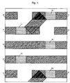
Fig. 1 zeigt in einer Draufsicht auf eine Metallisierungsebene
Leiterbahnen 10 bis 15, von denen die Leiterbahnen 10, 11
sowie 14 und 15 einander jeweils in einem Twist-Bereich überkreuzen.
Das heißt, die Leitung 10 ist in einer über der Metallisierungsebene
der Fig. 1 liegenden weiteren Ebene im Abstand
und getrennt durch eine Isolierschicht über die Leiterbahn
11 geführt. Die Leiterbahnen 12 und 13 sind dagegen
durchgehende Leiterbahnen.1 shows a top view of a metallization level
Conductor tracks 10 to 15, of which the conductor tracks 10, 11
and 14 and 15 cross each other in a twist area.
That is,
Die Leiterbahnen 14 und 15 weisen eine ähnliche Struktur wie die Leiterbahnen 10 und 11 auf.The conductor tracks 14 and 15 have a similar structure as the conductor tracks 10 and 11.
Bei diesen Leiterbahnen 10 bis 15 kann es sich beispielsweise um Bitleitungen eines Speicherzellenfeldes handeln. Die Breite der Leiterbahnen liegt zwischen 150 bis 250 nm und beträgt vorzugsweise etwa 200 nm. Der Abstand zwischen den Leiterbahnen liegt zwischen 130 und 180 nm. Die Leiterbahnen selbst können aus Aluminium oder Kupfer oder sonstigen geeigneten Materialien bestehen.These conductor tracks 10 to 15 can be, for example are bit lines of a memory cell array. The width the conductor paths lie between 150 and 250 nm and is preferably about 200 nm. The distance between the conductor tracks lies between 130 and 180 nm. The conductor tracks themselves can be made of aluminum or copper or other suitable Materials exist.
Es hat sich gezeigt, daß bei der Metallisierung der Leiterbahnen
10 bis 15 infolge des Proximity-Effektes kritische
Stellen dort entstehen, wo Diskontinuitäten in der Nachbarschaft
der Leiterbahnen vorliegen. Solche Diskontinuitäten
treten dann auf, wenn die benachbarte Leiterbahn unterbrochen
ist. An diesen diskontinuierlichen Stellen weisen die Leiterbahnen
Instabilitäten auf, die sogar zu einem Abriß der Leiterbahnen
führen können.It has been shown that in the metallization of the
Erfindungsgemäß sind nun an diesen kritischen Stellen Dummy-Kontakte
16 bis 20 vorgesehen, die zu einer unterhalb der
Leiterbahnebene der Fig. 1 liegenden Ebene führen.According to the invention, dummy contacts are now at these
Fig. 2 zeigt einen Schnitt durch einen solchen Dummy-Kontakt,
beispielsweise den Dummy-Kontakt 17. Die Leiterbahn 11 hat
hier in folge der diskontinuierlichen Nachbarschaft einen
verringerten Querschnitt, der, wie in Fig. 2 gezeigt ist, gegebenenfalls
auch beidseitig auftreten kann. Zur Verstärkung
der Leiterbahn 11 ist daher unterhalb von dieser der Dummy-Kontakt
17 vorgesehen, der eine Isolierschicht 5 aus Siliziumdioxid
durchsetzt und bis zu einer tieferliegenden Leiterbahnebene
21 führt. Auf dieser Leiterbahnebene 21 können zusätzliche
Leiterbahnen 22 verlaufen, die auf einer Siliziumdioxidschicht
23 liegen und von dem Dummy-Kontakt 17 elektrisch
isoliert sind.2 shows a section through such a dummy contact,
for example the
Wesentlich an der vorliegenden Erfindung ist also, daß Leiterbahnen an kritischen Stellen bewußt mit Dummy-Kontakten versehen werden, so daß eine Instabilität der Leiterbahn bzw. deren Abriß zuverlässig zu vermeiden sind. Diese Dummy-Kontakte brauchen selbstverständlich nicht bis zur nächsten Leiterbahnebene zu reichen. Es ist vielmehr ausreichend, wenn die Dummy-Kontakte einen solchen Querschnitt aufweisen, daß eine Instabilität bzw. ein Abriß der durch sie verstärkten Leiterbahn zuverlässig ausgeschlossen werden kann.It is therefore essential to the present invention that conductor tracks consciously at critical points with dummy contacts be provided so that instability of the conductor track or the demolition of which can be reliably avoided. These dummy contacts need of course not to the next conductor level to reach. Rather, it is sufficient if the dummy contacts have a cross section such that an instability or a demolition of those reinforced by it Conductor can be reliably excluded.
Claims (6)
dadurch gekennzeichnet, daß die Leiterbahnen (11 bis 15) an durch ihr Layout bedingten kritischen Stellen durch einen Dummy-Kontakt (16 bis 20) unterlegt sind.Integrated semiconductor circuit arrangement with conductor tracks (11 to 15; 22) running in at least two different planes, in which conductor tracks (11 to 15) are provided in close proximity, essentially parallel to one another, in at least one of the planes,
characterized in that the conductor tracks (11 to 15) are underpinned by a dummy contact (16 to 20) at critical points caused by their layout.
dadurch gekennzeichnet, daß die Dummy-Kontakte (16 bis 20) an kritischen Stellen vorgesehen sind, die durch eine Unterbrechung einer von zwei eng benachbarten parallelen Leiterbahnen bedingt sind.Integrated semiconductor circuit arrangement according to Claim 1,
characterized in that the dummy contacts (16 to 20) are provided at critical points which are caused by an interruption of one of two closely adjacent parallel conductor tracks.
dadurch gekennzeichnet, daß die Leiterbahnen eine Breite von 150 bis 250 nm haben.Integrated semiconductor circuit arrangement according to Claim 1 or 2,
characterized in that the conductor tracks have a width of 150 to 250 nm.
dadurch gekennzeichnet, daß die Leiterbahnen eine Breite von 200 nm haben.Integrated semiconductor circuit arrangement according to Claim 3,
characterized in that the conductor tracks have a width of 200 nm.
dadurch gekennzeichnet, daß der Abstand zwischen den Leiterbahnen (11 bis 15) 130 bis 180 nm beträgt. Integrated semiconductor circuit arrangement according to one of Claims 1 to 4,
characterized in that the distance between the conductor tracks (11 to 15) is 130 to 180 nm.
dadurch gekennzeichnet, daß die Leiterbahnen aus Aluminium oder Kupfer bestehen.Integrated semiconductor circuit arrangement according to one of Claims 1 to 5,
characterized in that the conductor tracks consist of aluminum or copper.
Applications Claiming Priority (2)
| Application Number | Priority Date | Filing Date | Title |
|---|---|---|---|
| DE19907127 | 1999-02-19 | ||
| DE19907127A DE19907127C1 (en) | 1999-02-19 | 1999-02-19 | Integrated semiconductor circuit arrangement with stabilized conductor tracks |
Publications (3)
| Publication Number | Publication Date |
|---|---|
| EP1030367A2 true EP1030367A2 (en) | 2000-08-23 |
| EP1030367A3 EP1030367A3 (en) | 2003-05-02 |
| EP1030367B1 EP1030367B1 (en) | 2005-05-04 |
Family
ID=7898136
Family Applications (1)
| Application Number | Title | Priority Date | Filing Date |
|---|---|---|---|
| EP00102589A Expired - Lifetime EP1030367B1 (en) | 1999-02-19 | 2000-02-07 | Integrated semiconductor device with stabilized conductive lines |
Country Status (6)
| Country | Link |
|---|---|
| US (1) | US6281586B1 (en) |
| EP (1) | EP1030367B1 (en) |
| JP (1) | JP2000243837A (en) |
| KR (1) | KR100366272B1 (en) |
| DE (2) | DE19907127C1 (en) |
| TW (1) | TW457686B (en) |
Cited By (2)
| Publication number | Priority date | Publication date | Assignee | Title |
|---|---|---|---|---|
| EP1032043A2 (en) | 1999-02-26 | 2000-08-30 | Infineon Technologies AG | Semiconductor memory device with twisted bit lines |
| DE10308924B3 (en) * | 2003-02-28 | 2004-10-28 | Infineon Technologies Ag | Integrated semiconductor circuit with a large number of memory cells |
Families Citing this family (2)
| Publication number | Priority date | Publication date | Assignee | Title |
|---|---|---|---|---|
| US6717268B2 (en) * | 2001-11-13 | 2004-04-06 | Intel Corporation | Electromigration-reliability improvement of dual damascene interconnects |
| US8796855B2 (en) | 2012-01-13 | 2014-08-05 | Freescale Semiconductor, Inc. | Semiconductor devices with nonconductive vias |
Citations (7)
| Publication number | Priority date | Publication date | Assignee | Title |
|---|---|---|---|---|
| EP0407933A2 (en) * | 1989-07-10 | 1991-01-16 | Nec Corporation | Resin sealed semiconductor device with improved thermal stress resistance |
| JPH0774176A (en) * | 1993-08-31 | 1995-03-17 | Sony Corp | Al wiring structure and formation thereof |
| EP0692824A2 (en) * | 1994-07-15 | 1996-01-17 | Texas Instruments Incorporated | Improvements in and relating to semiconductor devices |
| JPH0897290A (en) * | 1994-09-28 | 1996-04-12 | Kawasaki Steel Corp | Method for designing layout of semiconductor integrated circuit chip, and semiconductor integrated circuit chip |
| JPH09293721A (en) * | 1995-12-15 | 1997-11-11 | Lsi Logic Corp | Method for improving pattern design for integrated circuit structure processing |
| JPH10154808A (en) * | 1996-11-25 | 1998-06-09 | Toshiba Corp | Semiconductor device and manufacture thereof |
| JPH11154679A (en) * | 1997-11-20 | 1999-06-08 | Hitachi Ltd | Semiconductor device |
Family Cites Families (9)
| Publication number | Priority date | Publication date | Assignee | Title |
|---|---|---|---|---|
| JPS61194747A (en) * | 1985-02-22 | 1986-08-29 | Mitsubishi Electric Corp | Resin seal type semiconductor integrated circuit device |
| US6109775A (en) * | 1991-07-19 | 2000-08-29 | Lsi Logic Corporation | Method for adjusting the density of lines and contact openings across a substrate region for improving the chemical-mechanical polishing of a thin-film later disposed thereon |
| JP3141486B2 (en) * | 1992-01-27 | 2001-03-05 | ソニー株式会社 | Semiconductor device |
| JPH05206298A (en) * | 1992-01-28 | 1993-08-13 | Fujitsu Ltd | Manufacture of semiconductor device |
| JP3277098B2 (en) * | 1994-07-26 | 2002-04-22 | 株式会社東芝 | Method for manufacturing semiconductor device |
| JP3454970B2 (en) * | 1995-05-24 | 2003-10-06 | 富士通株式会社 | Mask pattern correction method, pattern formation method, and photomask |
| JP3457123B2 (en) * | 1995-12-07 | 2003-10-14 | 株式会社リコー | Semiconductor device |
| JP2923912B2 (en) * | 1996-12-25 | 1999-07-26 | 日本電気株式会社 | Semiconductor device |
| JP3093674B2 (en) * | 1997-04-07 | 2000-10-03 | 株式会社東芝 | Semiconductor device |
-
1999
- 1999-02-19 DE DE19907127A patent/DE19907127C1/en not_active Expired - Fee Related
-
2000
- 2000-02-07 DE DE50010202T patent/DE50010202D1/en not_active Expired - Fee Related
- 2000-02-07 EP EP00102589A patent/EP1030367B1/en not_active Expired - Lifetime
- 2000-02-11 TW TW089102306A patent/TW457686B/en active
- 2000-02-16 JP JP2000038349A patent/JP2000243837A/en active Pending
- 2000-02-16 KR KR1020000007242A patent/KR100366272B1/en not_active IP Right Cessation
- 2000-02-22 US US09/510,637 patent/US6281586B1/en not_active Expired - Fee Related
Patent Citations (7)
| Publication number | Priority date | Publication date | Assignee | Title |
|---|---|---|---|---|
| EP0407933A2 (en) * | 1989-07-10 | 1991-01-16 | Nec Corporation | Resin sealed semiconductor device with improved thermal stress resistance |
| JPH0774176A (en) * | 1993-08-31 | 1995-03-17 | Sony Corp | Al wiring structure and formation thereof |
| EP0692824A2 (en) * | 1994-07-15 | 1996-01-17 | Texas Instruments Incorporated | Improvements in and relating to semiconductor devices |
| JPH0897290A (en) * | 1994-09-28 | 1996-04-12 | Kawasaki Steel Corp | Method for designing layout of semiconductor integrated circuit chip, and semiconductor integrated circuit chip |
| JPH09293721A (en) * | 1995-12-15 | 1997-11-11 | Lsi Logic Corp | Method for improving pattern design for integrated circuit structure processing |
| JPH10154808A (en) * | 1996-11-25 | 1998-06-09 | Toshiba Corp | Semiconductor device and manufacture thereof |
| JPH11154679A (en) * | 1997-11-20 | 1999-06-08 | Hitachi Ltd | Semiconductor device |
Non-Patent Citations (5)
| Title |
|---|
| PATENT ABSTRACTS OF JAPAN vol. 1995, no. 06, 31. Juli 1995 (1995-07-31) -& JP 07 074176 A (SONY CORP), 17. März 1995 (1995-03-17) * |
| PATENT ABSTRACTS OF JAPAN vol. 1996, no. 08, 30. August 1996 (1996-08-30) -& JP 08 097290 A (KAWASAKI STEEL CORP), 12. April 1996 (1996-04-12) * |
| PATENT ABSTRACTS OF JAPAN vol. 1998, no. 11, 30. September 1998 (1998-09-30) -& JP 10 154808 A (TOSHIBA CORP), 9. Juni 1998 (1998-06-09) * |
| PATENT ABSTRACTS OF JAPAN vol. 1999, no. 07, 31. März 1999 (1999-03-31) -& JP 09 293721 A (LSI LOGIC CORP), 11. November 1997 (1997-11-11) -& US 6 109 775 A (PRABHAKAR TRIPATHI ET AL) 29. August 2000 (2000-08-29) * |
| PATENT ABSTRACTS OF JAPAN vol. 1999, no. 11, 30. September 1999 (1999-09-30) -& JP 11 154679 A (HITACHI LTD), 8. Juni 1999 (1999-06-08) * |
Cited By (2)
| Publication number | Priority date | Publication date | Assignee | Title |
|---|---|---|---|---|
| EP1032043A2 (en) | 1999-02-26 | 2000-08-30 | Infineon Technologies AG | Semiconductor memory device with twisted bit lines |
| DE10308924B3 (en) * | 2003-02-28 | 2004-10-28 | Infineon Technologies Ag | Integrated semiconductor circuit with a large number of memory cells |
Also Published As
| Publication number | Publication date |
|---|---|
| DE50010202D1 (en) | 2005-06-09 |
| KR20000062555A (en) | 2000-10-25 |
| TW457686B (en) | 2001-10-01 |
| EP1030367A3 (en) | 2003-05-02 |
| JP2000243837A (en) | 2000-09-08 |
| DE19907127C1 (en) | 2000-08-10 |
| US6281586B1 (en) | 2001-08-28 |
| EP1030367B1 (en) | 2005-05-04 |
| KR100366272B1 (en) | 2002-12-31 |
Similar Documents
| Publication | Publication Date | Title |
|---|---|---|
| DE102005047104B3 (en) | Semiconductor device with interconnected cell strips | |
| DE60022417T2 (en) | Flexible flat cable with earth conductors | |
| DE102016216702B4 (en) | amplifier | |
| WO2009138168A1 (en) | Circuit board for electrical connector and electrical connector | |
| DE3145039A1 (en) | INTEGRATED SEMICONDUCTOR CIRCUIT | |
| DE2536270A1 (en) | SEMI-CONDUCTOR DISC WITH MII OPENINGS | |
| DE2542518B2 (en) | POWER SUPPLY SYSTEM FOR HIGHLY INTEGRATED SEMICONDUCTOR CIRCUITS | |
| DE19519796C2 (en) | Semiconductor circuit with an overvoltage protection circuit | |
| DE69726190T2 (en) | METHOD FOR ARRANGING SIGNAL AND TARGET CONTACT AREAS FOR REALIZING SEVERAL SIGNAL / TARGET COMBINATIONS | |
| DE102014113465A1 (en) | Electronic component | |
| EP1030367A2 (en) | Integrated semiconductor device with stabilized conductive lines | |
| DE19908428C2 (en) | Semiconductor memory device with bit line twist | |
| DE4327290C2 (en) | Integrated semiconductor circuit | |
| EP0057253A2 (en) | System carrier tape with a plurality of system carriers for integrated circuits | |
| DE3434664C2 (en) | ||
| DE19916077A1 (en) | Fuse layout structure for DRAM, SRAM | |
| EP1075027A2 (en) | Contacting of metal interconnections of integrated semiconductor chips | |
| EP1231638B1 (en) | Power supply wiring of an integrated circuit | |
| DE10344605B4 (en) | Interconnect connection structure and related manufacturing process | |
| WO2003096419A2 (en) | Integrated strip conductor arrangement | |
| DE2522984C2 (en) | Electronic crosspoint module | |
| DE2808833C2 (en) | Printed circuit, especially foil wiring | |
| EP1398834A2 (en) | Electronic device with voltage supply structure and method of producing it | |
| DE3210998C2 (en) | ||
| DE10026933C1 (en) | Faraday cage for integrated circuit has lower and upper metallization planes filled with metallization layers and connected at edges by metal ring structures in intermediate planes |
Legal Events
| Date | Code | Title | Description |
|---|---|---|---|
| PUAI | Public reference made under article 153(3) epc to a published international application that has entered the european phase |
Free format text: ORIGINAL CODE: 0009012 |
|
| AK | Designated contracting states |
Kind code of ref document: A2 Designated state(s): AT BE CH CY DE DK ES FI FR GB GR IE IT LI LU MC NL PT SE |
|
| AX | Request for extension of the european patent |
Free format text: AL;LT;LV;MK;RO;SI |
|
| PUAL | Search report despatched |
Free format text: ORIGINAL CODE: 0009013 |
|
| AK | Designated contracting states |
Designated state(s): AT BE CH CY DE DK ES FI FR GB GR IE IT LI LU MC NL PT SE |
|
| AX | Request for extension of the european patent |
Extension state: AL LT LV MK RO SI |
|
| RIC1 | Information provided on ipc code assigned before grant |
Ipc: 7H 01L 23/522 A Ipc: 7H 01L 23/528 B |
|
| 17P | Request for examination filed |
Effective date: 20031022 |
|
| 17Q | First examination report despatched |
Effective date: 20031119 |
|
| AKX | Designation fees paid |
Designated state(s): DE GB IE |
|
| GRAP | Despatch of communication of intention to grant a patent |
Free format text: ORIGINAL CODE: EPIDOSNIGR1 |
|
| GRAS | Grant fee paid |
Free format text: ORIGINAL CODE: EPIDOSNIGR3 |
|
| GRAA | (expected) grant |
Free format text: ORIGINAL CODE: 0009210 |
|
| AK | Designated contracting states |
Kind code of ref document: B1 Designated state(s): DE GB IE |
|
| REG | Reference to a national code |
Ref country code: GB Ref legal event code: FG4D Free format text: NOT ENGLISH |
|
| REG | Reference to a national code |
Ref country code: IE Ref legal event code: FG4D Free format text: LANGUAGE OF EP DOCUMENT: GERMAN |
|
| REF | Corresponds to: |
Ref document number: 50010202 Country of ref document: DE Date of ref document: 20050609 Kind code of ref document: P |
|
| GBT | Gb: translation of ep patent filed (gb section 77(6)(a)/1977) |
Effective date: 20050802 |
|
| PLBE | No opposition filed within time limit |
Free format text: ORIGINAL CODE: 0009261 |
|
| STAA | Information on the status of an ep patent application or granted ep patent |
Free format text: STATUS: NO OPPOSITION FILED WITHIN TIME LIMIT |
|
| 26N | No opposition filed |
Effective date: 20060207 |
|
| PGFP | Annual fee paid to national office [announced via postgrant information from national office to epo] |
Ref country code: GB Payment date: 20080220 Year of fee payment: 9 Ref country code: IE Payment date: 20080220 Year of fee payment: 9 |
|
| PGFP | Annual fee paid to national office [announced via postgrant information from national office to epo] |
Ref country code: DE Payment date: 20080415 Year of fee payment: 9 |
|
| GBPC | Gb: european patent ceased through non-payment of renewal fee |
Effective date: 20090207 |
|
| REG | Reference to a national code |
Ref country code: IE Ref legal event code: MM4A |
|
| PG25 | Lapsed in a contracting state [announced via postgrant information from national office to epo] |
Ref country code: IE Free format text: LAPSE BECAUSE OF NON-PAYMENT OF DUE FEES Effective date: 20090209 Ref country code: DE Free format text: LAPSE BECAUSE OF NON-PAYMENT OF DUE FEES Effective date: 20090901 |
|
| PG25 | Lapsed in a contracting state [announced via postgrant information from national office to epo] |
Ref country code: GB Free format text: LAPSE BECAUSE OF NON-PAYMENT OF DUE FEES Effective date: 20090207 |