EP1028367A1 - Anordnung und Verfahren für die Verbesserung der Schreibleistung einer Rechnerdatenspeicherperipherie - Google Patents
Anordnung und Verfahren für die Verbesserung der Schreibleistung einer Rechnerdatenspeicherperipherie Download PDFInfo
- Publication number
- EP1028367A1 EP1028367A1 EP00400299A EP00400299A EP1028367A1 EP 1028367 A1 EP1028367 A1 EP 1028367A1 EP 00400299 A EP00400299 A EP 00400299A EP 00400299 A EP00400299 A EP 00400299A EP 1028367 A1 EP1028367 A1 EP 1028367A1
- Authority
- EP
- European Patent Office
- Prior art keywords
- data
- memory
- volatile
- written
- backup
- Prior art date
- Legal status (The legal status is an assumption and is not a legal conclusion. Google has not performed a legal analysis and makes no representation as to the accuracy of the status listed.)
- Withdrawn
Links
Images

Classifications
-
- G—PHYSICS
- G06—COMPUTING; CALCULATING OR COUNTING
- G06F—ELECTRIC DIGITAL DATA PROCESSING
- G06F11/00—Error detection; Error correction; Monitoring
- G06F11/07—Responding to the occurrence of a fault, e.g. fault tolerance
- G06F11/14—Error detection or correction of the data by redundancy in operation
- G06F11/1402—Saving, restoring, recovering or retrying
- G06F11/1415—Saving, restoring, recovering or retrying at system level
- G06F11/1441—Resetting or repowering
-
- G—PHYSICS
- G06—COMPUTING; CALCULATING OR COUNTING
- G06F—ELECTRIC DIGITAL DATA PROCESSING
- G06F11/00—Error detection; Error correction; Monitoring
- G06F11/07—Responding to the occurrence of a fault, e.g. fault tolerance
- G06F11/16—Error detection or correction of the data by redundancy in hardware
- G06F11/1666—Error detection or correction of the data by redundancy in hardware where the redundant component is memory or memory area
-
- G—PHYSICS
- G11—INFORMATION STORAGE
- G11C—STATIC STORES
- G11C29/00—Checking stores for correct operation ; Subsequent repair; Testing stores during standby or offline operation
- G11C29/70—Masking faults in memories by using spares or by reconfiguring
- G11C29/74—Masking faults in memories by using spares or by reconfiguring using duplex memories, i.e. using dual copies
-
- G—PHYSICS
- G06—COMPUTING; CALCULATING OR COUNTING
- G06F—ELECTRIC DIGITAL DATA PROCESSING
- G06F11/00—Error detection; Error correction; Monitoring
- G06F11/07—Responding to the occurrence of a fault, e.g. fault tolerance
- G06F11/16—Error detection or correction of the data by redundancy in hardware
- G06F11/20—Error detection or correction of the data by redundancy in hardware using active fault-masking, e.g. by switching out faulty elements or by switching in spare elements
-
- G—PHYSICS
- G06—COMPUTING; CALCULATING OR COUNTING
- G06F—ELECTRIC DIGITAL DATA PROCESSING
- G06F3/00—Input arrangements for transferring data to be processed into a form capable of being handled by the computer; Output arrangements for transferring data from processing unit to output unit, e.g. interface arrangements
- G06F3/06—Digital input from, or digital output to, record carriers, e.g. RAID, emulated record carriers or networked record carriers
- G06F3/0601—Interfaces specially adapted for storage systems
- G06F3/0602—Interfaces specially adapted for storage systems specifically adapted to achieve a particular effect
- G06F3/061—Improving I/O performance
- G06F3/0613—Improving I/O performance in relation to throughput
-
- G—PHYSICS
- G06—COMPUTING; CALCULATING OR COUNTING
- G06F—ELECTRIC DIGITAL DATA PROCESSING
- G06F3/00—Input arrangements for transferring data to be processed into a form capable of being handled by the computer; Output arrangements for transferring data from processing unit to output unit, e.g. interface arrangements
- G06F3/06—Digital input from, or digital output to, record carriers, e.g. RAID, emulated record carriers or networked record carriers
- G06F3/0601—Interfaces specially adapted for storage systems
- G06F3/0602—Interfaces specially adapted for storage systems specifically adapted to achieve a particular effect
- G06F3/0614—Improving the reliability of storage systems
- G06F3/0619—Improving the reliability of storage systems in relation to data integrity, e.g. data losses, bit errors
-
- G—PHYSICS
- G06—COMPUTING; CALCULATING OR COUNTING
- G06F—ELECTRIC DIGITAL DATA PROCESSING
- G06F3/00—Input arrangements for transferring data to be processed into a form capable of being handled by the computer; Output arrangements for transferring data from processing unit to output unit, e.g. interface arrangements
- G06F3/06—Digital input from, or digital output to, record carriers, e.g. RAID, emulated record carriers or networked record carriers
- G06F3/0601—Interfaces specially adapted for storage systems
- G06F3/0628—Interfaces specially adapted for storage systems making use of a particular technique
- G06F3/0655—Vertical data movement, i.e. input-output transfer; data movement between one or more hosts and one or more storage devices
- G06F3/0656—Data buffering arrangements
-
- G—PHYSICS
- G06—COMPUTING; CALCULATING OR COUNTING
- G06F—ELECTRIC DIGITAL DATA PROCESSING
- G06F3/00—Input arrangements for transferring data to be processed into a form capable of being handled by the computer; Output arrangements for transferring data from processing unit to output unit, e.g. interface arrangements
- G06F3/06—Digital input from, or digital output to, record carriers, e.g. RAID, emulated record carriers or networked record carriers
- G06F3/0601—Interfaces specially adapted for storage systems
- G06F3/0668—Interfaces specially adapted for storage systems adopting a particular infrastructure
- G06F3/0671—In-line storage system
- G06F3/0673—Single storage device
- G06F3/0679—Non-volatile semiconductor memory device, e.g. flash memory, one time programmable memory [OTP]
Definitions
- the subject of the present invention is a method for writing data. digital devices on a data storage device.
- a storage device comprises storage means which can be either a magnetic tape, an optical disc, a magnetic disk, hard disk, floppy disk or floppy disk, or any other high capacity data storage medium. These different means of storage belong to the family of so-called mass memories given the large capacity of these compared to the semiconductor memories of volatile RAM (Random Access Memory) or cache type, and non-volatile type, for example a ROM family (Read Only Memory) such an EEPROM (Electrically Eraseable Programmable Read Only) memory Memory), an EPROM (Electrically Programmable Read Only) memory Memory) Flash, etc. Volatile semiconductor memories are used to temporarily store data.
- the storage device includes a cache used both in reading and writing.
- a cache is known for its properties of very short access time and acceleration of data processing. In write, this cache serves as a buffer better known as name of ⁇ buffer ⁇ for a person skilled in the art. In reading, a cache memory stores data to which access is expected soon.
- the computer system may include one or more multiple storage devices.
- a storage device may include one or more storage means.
- the choice of storage means depends on the information to store on it.
- This storage means will, in the example chosen, a magnetic disc.
- the storage constitutes a system ensuring high data integrity.
- the data to be written comes from a host system.
- This host system includes at least one microprocessor and memories of any type related to it.
- the result is a computer system for implementing the method.
- Writing data to a storage medium such as disks magnetic is successively preceded by a writing of this data in a memory of the host system and in a volatile memory of the storage device.
- the volatile memory of the device storage is a cache.
- a storage device is characterized, in addition to its high protection of data integrity, both by its access time to the data sought on the storage medium and by its writing time data to be stored on the storage medium.
- the access time for example for a storage medium powerful magnetic disc type, can be evaluated on average at 14-15 ms. This access time can exceed 25 ms depending on the case.
- the big problem is that the host system will have to keep in its memory the data being written until it is actually written to the means of storage. If an incident occurs, preventing writing partially or all of the data, it will be absolutely necessary to find these data and rewrite it in the intended location.
- One solution is to use a function providing a message of write termination on the storage device cache.
- This function is authorized in the storage device by positioning a certain flag in the write command from the host system. The positioning the indicator at a certain value, 0 or 1, allows you to use disk cache as initiator of the termination message writing.
- this function presents a second problem.
- the disk sends towards the host system a message for the correct termination of the write request as soon as the data are stored in the disk cache (access operations being hidden).
- the problem is that if a drive crash or a crash disc power occurs between the time the disc is wound up correct termination information to the host and when all of the information is written physically on the storage medium, there is loss of data. This is unacceptable in an area where data integrity is the centerpiece and therefore where data loss is not possible.
- Another solution to the first problem is to incorporate an element additional in the chain, constituted by the host system and the storage device, such as a disk controller card.
- the disk controller capable of supporting RAID functions (Redundant Array on an Inexpensive Disks) or not.
- a cache associated with the controller will keep the data being written in place of the memory associated with the host system.
- This solution imposes a cost in money important in that it will pay the controller function, pay the cache memory and above all make sure that the function supports a failure without risk of information loss.
- Most of the time we use memory backed up by battery with a limited duration, or storage of redundant data such as in RAID systems (Redundant Array of Independent Disks) known to those skilled in the art. This type of storage requires backing up data on specific disk areas (with also a battery), etc. All this has a significant cost without counting adding a link in the chain adds a few milliseconds response time.
- Another solution is to set up the fast writing solution on disks in a secure manner as described in the request for Applicant's patent No. 98 13987.
- This implementation requires hardware at the storage device and software above the driver.
- a first goal is to increase the writing performance of a computer system while providing the system with high protection from data integrity.
- a second goal is the possibility of writing data on the means of storage without slowing down the performance of the host system.
- Another goal is to significantly reduce the cost of money of such an implementation.
- the subject of the invention is, in a computer system, a method for writing data to at least one storage device for data including at least one data storage means and at least one volatile memory serving as a buffer including the data to be written to at least said storage means, the system comprising at least one host system connected to at least said storage device via links to exchange information between them, including data to be written on at least said storage device, the host system comprising at least one memory which can contain the data to be written to at least said storage means, the method comprising a request writing consisting in issuing a write command on one of said connections and is characterized in that it consists in safeguarding, by through at least one non-volatile data backup means, the data to be written to said at least one storage means during at least minus the duration of writing of this data on said at least one means of storage and what it consists of, following this backup, to be transmitted to host system a data write termination message in at least said means for saving non-volatile data.
- the result is a computer system comprising at least one data storage device including at least one storage means data and at least volatile memory serving as a buffer including the data to be written to at least said storage means, the system comprising at least one host system connected to said at least one peripheral storage via links to exchange information including data to write on at least said storage device, the host system comprising at least one memory may contain the data to be written to at least said storage means, a write request consisting in issuing a write command on a of said connections, characterized in that the volatile memory is substituted for the at least one non-volatile memory or is connected to at least one non-volatile memory to constitute a non-volatile safeguard.
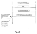
- a SYS computer system has been represented. including a SH host system and a PER storage device.
- the host system SH and a storage device PER are linked together, for example via a SCSI bus.
- the computer system can include multiple storage devices.
- the PER storage device clearly understands on a SCSI (Small Computer System Interface) type interface. So generally, the nature of the interface depends on the nature of the bus B1 used. We can find different types of interfaces such as a SCSI interface (Small Computer System Interface), FC-AL (Fiber Channel-Arbitred Loop), P1394 (firewire, Serial Bus), ATA (Advanced Technology Attachment), etc. He is known that the interface allows standardized high speed connections between a host system and the various devices to which it is connected.
- This PER device includes a volatile memory MV1, preferably a memory commonly called cache memory (also called cache memory), known to those skilled in the art. In the following description, we will use the cache term to designate this type of memory.
- this memory is used for both reading and writing; a memory area is therefore dedicated to writing data on said storage means and an area memory is dedicated to reading data.
- This MV1 cache is a memory whose access time is very short compared to other memories existing. This cache temporarily stores data to be written to a means of storage.
- All elements of the PER storage device are powered by at least one ALIM power source.
- a PRO microprocessor connected to at least one MP firmware needed to run all microprocessor instructions.
- This microprocessor is connected by links respective LI1-LI3 at the INT interface, at memory MV1 and at the various components of the LEC reader. To simplify the description, the links connecting the microprocessor to the various components of the LEC reader are represented in Figure 1 via a single LI3 link.
- the INT interface receives as input the SCSI bus which includes several lines. The description of different lines are given in the following description.
- a B2 bus from data links the interface output to the input of the MV1 cache memory.
- Another bus B3 connects the output of the cache memory MV1 to the input of the reader constituted by the set of CEL boxes.
- a B4 bus connects the output of the set of CEL boxes with POS positioning system.
- the SH host system also includes any memory MV2 in which we store data to write on the PER device. For reasons of simplification of the description, we have not shown the other building blocks of the host system. This MV2 memory is also controlled via a microprocessor associated with at least one firmware, not shown in the figure.
- the SH host system includes a B5 bus, for example of the PCI type (Peripheral Component Interconnect). A bus adapter ensures connection of the PCI bus to bus B1 of type SCSI.
- PCI type Peripheral Component Interconnect
- the big problem is that the SH host system will have to keep in its memory MV2 the data being written until it is actually written to the STO storage medium. As mentioned in the introduction, if an incident occurs, preventing the writing of all or part of the data, it will be absolutely necessary to rewrite them in the space provided if the defect was passenger. Having records for the SH host system keep in memory MV2 for very long times compared to its calculation speed, slows it down and therefore limits its performances.
- a solution to this problem consists, through at least one MEM non-volatile data backup means, to save the data to write for at least the duration of writing of this data on said at least one STO storage means, and in that it consists of transmitting, to the SH host system, a data write termination message.
- the MV2 memory of SH host system becomes available for storage of new data upon receipt of the write completion message from data on said at least one non-volatile data backup means SAME.
- the solution therefore consists in making the memory MV1 non-volatile.
- the volatile memory MV1 is used in writing and reading.
- the solution consists in making at least the memory area dedicated to non-volatile writing. More precisely, it consists in making the memory area which stores non-volatile the data to be written to the storage medium. It can be obtained from various ways using, in place of the memory MV1, at least one non-volatile memory or using non-volatile memories in combination with random access memory MV1.
- the solution consists in associating the cache memory MV1 has at least one non-volatile memory MEM.
- data is saved in at least one non-volatile memory of EEPROM type for at least the duration of writing of this data on the storage medium.
- the volatile memory MV1 is connected in parallel to a non-volatile memory EEPROM. It then consists in transmitting, to the host system SH, a message for terminating the writing of data in said non-volatile memory EEPROM.
- non-volatile memory is not limited to a EEPROM type memory but any other non-volatile device.
- a non-volatile memory is defined as any memory capable of retaining data in the event of a power failure.
- the association between a volatile memory and a non-volatile memory constitutes, for example, a memory of the NOVRAM type (Non-volatile Random Access Memory) known to those skilled in the art.
- This guy of memory incorporates RAM cells (Random Access Memory) and EEPROM cells.
- this non-volatile memory receives as input the same information that volatile memory receives MV1.
- the data is systematically saved in the cache MV1 and in the non-volatile memory EEPROM.
- data is stored in non-volatile memory EEPROM only when the fault is detected. In the latter case, the backup reaction time should be very short.
- the memory MV1 is connected to one (or more) voltage supervisor who ensures switching automatic memory MV1 on a backup battery in case of mains voltage cut.
- the volatile memory MV1 is protected against writing during the voltage switching phase and the data are therefore kept.
- the backup battery or a battery must be able to supply energy for a sufficient time long corresponding to the duration of the breakdown and repair.
- the energy source for backing up data in the non-volatile memory can be, in another example, the recovery of the rotational energy of the discs. This eliminates the need for a battery or of a pile.
- the memory area of the memory MV2 of the host system SH including the data to be written to the STO storage means can therefore be released safely. So we can write new data to the free area of the MV2 memory of the SH host system even before the data is written to the medium STO storage.
- the solution includes several steps, including:
- a device failure includes, for example, a ALIM power which can be caused by a power failure drive, power failure, or improper handling by an operator following a disk extraction.
- the device When the fault is repaired and the power-up tests reveal a normal power supply, the device is again in a state of on and the data stored in the non-volatile memory MEM is transmitted for writing on the storage means. These data are written to the entire STO storage medium.
- the purpose of the solution is, in a system SYS computing, a method of writing data on at least one PER data storage device including at least one means of STO data storage and at least one volatile memory MV1 serving as buffer memory including the data to be written to at least said means of STO storage, the system comprising at least one SH host system connected to the minus said PER storage device through links for exchange information with each other including data to write on at least said storage device PER, the host system SH comprising at least one memory MV2 which can contain the data to be written on at least said storage means, the method comprising a request writing consisting in issuing a write command on one of said connections and is characterized in that it consists in safeguarding, by through at least one non-volatile data backup means MEM, the data to be written to said at least one storage means STO for at least the duration of writing of this data on said at least one STO storage medium and what it consists of, following this backup, transmit a write data termination message to the host system in at least said means for saving non
- the solution consists in receiving the message from termination of writing data to at least said backup means of non-volatile data MEM, to free the memory area of the memory MV2 of the host system including the data written on at least said means of MEM data backup.
- the solution therefore gives the possibility, after having freed the memory area of the memory MV2 of the host system SH, write new data to the MV2 memory of the host system even before the actual writing of data is completed on at least said storage means STO.
- Data backup consists, for through said at least one MEM backup means, to transform the volatile memory MV1 into non-volatile memory.
- This backup materializes in different ways.
- This backup on at least said storage means MEM may consist of store the data in at least one non-volatile memory of the type EEPROM.
- This backup on at least said storage means MEM can also consist in storing the data to be written on at least said means of storage in volatile memory MV1 equipped with a voltage supervisor to ensure automatic switching of this volatile memory MV1 to a backup battery.
- This backup on at least said means of MEM storage can also consist of storing the data to be written to at minus said means of storage in the volatile memory MV1 of the peripheral PER connected in parallel to at least one non-volatile memory.
- a SYS computer system comprising at least one PER data storage device including at least one means of STO data storage and at least volatile memory MV1 serving as buffer memory including the data to be written to said at least one means of STO storage, the system comprising at least one linked SH host system audit at least one PER storage device through links to exchange information with each other including data to be written on said at least one PER storage device, the SH host system comprising at least one memory MV2 which can contain the data to be written on said at least one storage means, a request writing consisting in issuing a write command on one of said connections, characterized in that the volatile memory MV1 is substituted for at least a non-volatile memory or is connected to at least one non-volatile memory to constitute a non-volatile MEM backup means.
- a write request includes an information bit suitable for validating a write termination software function in the backup means MEM data.
- the solution significantly increases the write performance of a storage device.
- the MV1 cache of the PER storage device is transformed into non-volatile memory according to one of the variants mentioned above. Data at risk of being lost are automatically stored in this non-volatile memory and written on the storage medium after repair. The problem of integrity data is resolved.
- Memory area of the host system MV2 memory including the data to be written is reusable upon receipt of the message from termination of the writing of the data on the backup means MEM.
- the response time to writing data is of the order of a millisecond.
- the host system therefore releases much more quickly its MV2 memory.
- the performance of the SH host system is therefore greatly improved.
- Another advantage is the cost extremely weak of such a solution. Depending on the solution chosen, the cost corresponds to non-volatile memory.
Applications Claiming Priority (2)
| Application Number | Priority Date | Filing Date | Title |
|---|---|---|---|
| FR9901649A FR2789777B1 (fr) | 1999-02-11 | 1999-02-11 | Dispositif et procede d'amelioration des performances en ecriture d'un peripherique de stockage de donnees pour ordinateur |
| FR9901649 | 1999-02-11 |
Publications (1)
| Publication Number | Publication Date |
|---|---|
| EP1028367A1 true EP1028367A1 (de) | 2000-08-16 |
Family
ID=9541898
Family Applications (1)
| Application Number | Title | Priority Date | Filing Date |
|---|---|---|---|
| EP00400299A Withdrawn EP1028367A1 (de) | 1999-02-11 | 2000-02-03 | Anordnung und Verfahren für die Verbesserung der Schreibleistung einer Rechnerdatenspeicherperipherie |
Country Status (3)
| Country | Link |
|---|---|
| EP (1) | EP1028367A1 (de) |
| JP (1) | JP2000242568A (de) |
| FR (1) | FR2789777B1 (de) |
Citations (2)
| Publication number | Priority date | Publication date | Assignee | Title |
|---|---|---|---|---|
| EP0721162A2 (de) * | 1995-01-06 | 1996-07-10 | Hewlett-Packard Company | Speicherplattenanordnung mit auf gespiegeltem Speicher basierten doppelten Steuergeräten |
| US5594909A (en) * | 1991-07-05 | 1997-01-14 | Nec Corporation | File I/O control device writing blocks to faster device first and canceling exclusive lock as each block is written |
-
1999
- 1999-02-11 FR FR9901649A patent/FR2789777B1/fr not_active Expired - Fee Related
-
2000
- 2000-02-03 EP EP00400299A patent/EP1028367A1/de not_active Withdrawn
- 2000-02-10 JP JP2000033455A patent/JP2000242568A/ja active Pending
Patent Citations (2)
| Publication number | Priority date | Publication date | Assignee | Title |
|---|---|---|---|---|
| US5594909A (en) * | 1991-07-05 | 1997-01-14 | Nec Corporation | File I/O control device writing blocks to faster device first and canceling exclusive lock as each block is written |
| EP0721162A2 (de) * | 1995-01-06 | 1996-07-10 | Hewlett-Packard Company | Speicherplattenanordnung mit auf gespiegeltem Speicher basierten doppelten Steuergeräten |
Also Published As
| Publication number | Publication date |
|---|---|
| FR2789777B1 (fr) | 2001-08-17 |
| FR2789777A1 (fr) | 2000-08-18 |
| JP2000242568A (ja) | 2000-09-08 |
Similar Documents
| Publication | Publication Date | Title |
|---|---|---|
| US6954834B2 (en) | Data backup including tape and non-volatile memory units and method of operating same | |
| FR2561428A1 (fr) | Procede d'enregistrement dans une memoire a disques et systeme de memoire a disques | |
| EP1044412A1 (de) | Vorrichtung und verfahren zum gesicherten schreiben in einem plattencachespeicher für festplatten eines massenspeichersubsystems | |
| JP3646303B2 (ja) | コンピュータシステムとそのメモリ管理方法、及びメモリ管理プログラムを記録した記録媒体 | |
| FR2726923A1 (fr) | Groupe redondant de dispositifs a memoire a semi-conducteurs | |
| FR2870367A1 (fr) | Systeme et procede de restauration de disque apres incident disque | |
| EP0434532B1 (de) | Sicheres Datenschnellschreibverfahren für Massenspeichereinrichtung und ein dieses Verfahren ausführendes Computersystem | |
| US6181630B1 (en) | Method of stabilizing data stored in volatile memory | |
| US9619330B2 (en) | Protecting volatile data of a storage device in response to a state reset | |
| FR2863734A1 (fr) | Systeme de reseau de disques et convertisseur d'interface | |
| FR2807532A1 (fr) | Dispositif et procede de memorisation de donnees de journalisation dans un reseau de communication | |
| FR2634917A1 (fr) | Procede et dispositif de protection d'un logiciel, en particulier contre les copies non autorisees | |
| BE1014650A6 (fr) | Systeme de realisation automatique de copies de sauvegarde de fichiers informatiques lorsqu'un ordinateur personnel est eteint. | |
| CN101859233B (zh) | 光盘装置 | |
| EP1028367A1 (de) | Anordnung und Verfahren für die Verbesserung der Schreibleistung einer Rechnerdatenspeicherperipherie | |
| EP1258004B1 (de) | Geschutztes echtzeit-schreiben in einen nichtflüchtigen speicher | |
| EP0918388B1 (de) | Elektrischer Fehlerschutz in einem Datenspeichersystem | |
| WO1995019002A1 (fr) | Procede de sauvegarde et/ou d'archivage de donnees et/ou de fichiers informatiques et dispositif pour la mise en ×uvre dudit procede | |
| EP1762939A1 (de) | Verfahren zur Speicherung von numerischen Daten in einem großen Informationssystem und zugehörige Vorrichtung | |
| EP2531921B1 (de) | Verwaltung des datenspeicherungsortes in einem verteilten speicherungssystem | |
| EP1818846A1 (de) | Verifizierung der Integrität von Programmen oder der Sequenzierung einer Zustandsmaschine | |
| EP2009570B1 (de) | Vorrichtung zur vorübergehenden Speicherung von Daten | |
| JPH0756790A (ja) | ネットワークデータバックアップ装置 | |
| JP2002313017A (ja) | データ記録装置 | |
| EP0459877A1 (de) | Rechensystem zur Datenübertragung im Stossbetrieb |
Legal Events
| Date | Code | Title | Description |
|---|---|---|---|
| PUAI | Public reference made under article 153(3) epc to a published international application that has entered the european phase |
Free format text: ORIGINAL CODE: 0009012 |
|
| AK | Designated contracting states |
Kind code of ref document: A1 Designated state(s): BE DE FR GB |
|
| AX | Request for extension of the european patent |
Free format text: AL;LT;LV;MK;RO;SI |
|
| 17P | Request for examination filed |
Effective date: 20010216 |
|
| AKX | Designation fees paid |
Free format text: BE DE FR GB |
|
| 17Q | First examination report despatched |
Effective date: 20030813 |
|
| STAA | Information on the status of an ep patent application or granted ep patent |
Free format text: STATUS: THE APPLICATION IS DEEMED TO BE WITHDRAWN |
|
| 18D | Application deemed to be withdrawn |
Effective date: 20031224 |