EP1022856A2 - Transmitting and receiving apparatus capable of the suppression of the microphonic noise in digital transmission system - Google Patents
Transmitting and receiving apparatus capable of the suppression of the microphonic noise in digital transmission system Download PDFInfo
- Publication number
- EP1022856A2 EP1022856A2 EP00100929A EP00100929A EP1022856A2 EP 1022856 A2 EP1022856 A2 EP 1022856A2 EP 00100929 A EP00100929 A EP 00100929A EP 00100929 A EP00100929 A EP 00100929A EP 1022856 A2 EP1022856 A2 EP 1022856A2
- Authority
- EP
- European Patent Office
- Prior art keywords
- frequency
- signal output
- signal
- amplifying
- modulating
- Prior art date
- Legal status (The legal status is an assumption and is not a legal conclusion. Google has not performed a legal analysis and makes no representation as to the accuracy of the status listed.)
- Granted
Links
Images






Classifications
-
- H—ELECTRICITY
- H03—ELECTRONIC CIRCUITRY
- H03L—AUTOMATIC CONTROL, STARTING, SYNCHRONISATION OR STABILISATION OF GENERATORS OF ELECTRONIC OSCILLATIONS OR PULSES
- H03L7/00—Automatic control of frequency or phase; Synchronisation
- H03L7/06—Automatic control of frequency or phase; Synchronisation using a reference signal applied to a frequency- or phase-locked loop
- H03L7/16—Indirect frequency synthesis, i.e. generating a desired one of a number of predetermined frequencies using a frequency- or phase-locked loop
- H03L7/18—Indirect frequency synthesis, i.e. generating a desired one of a number of predetermined frequencies using a frequency- or phase-locked loop using a frequency divider or counter in the loop
-
- H—ELECTRICITY
- H03—ELECTRONIC CIRCUITRY
- H03L—AUTOMATIC CONTROL, STARTING, SYNCHRONISATION OR STABILISATION OF GENERATORS OF ELECTRONIC OSCILLATIONS OR PULSES
- H03L1/00—Stabilisation of generator output against variations of physical values, e.g. power supply
-
- H—ELECTRICITY
- H03—ELECTRONIC CIRCUITRY
- H03L—AUTOMATIC CONTROL, STARTING, SYNCHRONISATION OR STABILISATION OF GENERATORS OF ELECTRONIC OSCILLATIONS OR PULSES
- H03L7/00—Automatic control of frequency or phase; Synchronisation
- H03L7/06—Automatic control of frequency or phase; Synchronisation using a reference signal applied to a frequency- or phase-locked loop
- H03L7/08—Details of the phase-locked loop
- H03L7/085—Details of the phase-locked loop concerning mainly the frequency- or phase-detection arrangement including the filtering or amplification of its output signal
- H03L7/093—Details of the phase-locked loop concerning mainly the frequency- or phase-detection arrangement including the filtering or amplification of its output signal using special filtering or amplification characteristics in the loop
-
- H—ELECTRICITY
- H03—ELECTRONIC CIRCUITRY
- H03L—AUTOMATIC CONTROL, STARTING, SYNCHRONISATION OR STABILISATION OF GENERATORS OF ELECTRONIC OSCILLATIONS OR PULSES
- H03L7/00—Automatic control of frequency or phase; Synchronisation
- H03L7/06—Automatic control of frequency or phase; Synchronisation using a reference signal applied to a frequency- or phase-locked loop
- H03L7/08—Details of the phase-locked loop
- H03L7/099—Details of the phase-locked loop concerning mainly the controlled oscillator of the loop
-
- H—ELECTRICITY
- H04—ELECTRIC COMMUNICATION TECHNIQUE
- H04L—TRANSMISSION OF DIGITAL INFORMATION, e.g. TELEGRAPHIC COMMUNICATION
- H04L5/00—Arrangements affording multiple use of the transmission path
- H04L5/02—Channels characterised by the type of signal
- H04L5/06—Channels characterised by the type of signal the signals being represented by different frequencies
Definitions
- the present invention relates to a transmitting and receiving apparatus which is to be mounted in a mobile unit such as an airplane, and particularly to a transmitting and receiving apparatus which digitally transmits a video and a sound.
- a digital video/audio system according to the MPEG standard is practically used in satellite broadcasting, a CATV, etc.
- an analog broadcasting system is mainly used at the present time.
- Such a system is desired to be replaced with a digital broadcasting system in which an image compression technique such as MPEG is combined with a digital modulation technique, so that the number of transmission channels is increased and services are individually provided to all seats (for example, Japanese Patent Publication (Kokai) No. HEI7-255043).
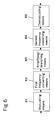
- Fig. 6 shows the configuration of a transmitting and receiving apparatus of the prior art.
- 61 denotes modulating means
- 62 denotes first frequency converting means
- 63 denotes amplifying/branching means
- 64 denotes second frequency converting means
- 65 denotes demodulating means.
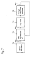
- Fig. 7 shows the configuration of a PLL frequency synthesizer included in each of the first and second frequency converting means 62 and 64.
- 71 denotes a PLL synthesizer IC
- 72 denotes a loop filter
- 73 denotes a voltage controlled oscillator
- 74 denotes a crystal oscillator.
- the modulating means 61 performs quadrature amplitude modulation (hereinafter, abbreviated as QAM modulation) which is used in a CATV and the like, or vestigial sideband modulation (hereinafter, abbreviated as VSB modulation) on the data and produces a signal of a center frequency f1.
- QAM modulation quadrature amplitude modulation
- VSB modulation vestigial sideband modulation
- a signal output from the modulating means 61 is input to the first frequency converting means 62.
- the center frequency of the input signal is converted from f1 to f2.
- a frequency in a frequency band of several tens to several hundreds MHz is usually used as the center frequency f2.
- a signal output from the first frequency converting means 62 is input to the amplifying/branching means 63.
- the amplifying/branching means 63 amplifies and branches the input signal, and outputs the amplified and branched signals in order to distribute the signals to various areas of the airplane.
- the signals output from the amplifying/branching means 63 are input to the second frequency converting means 64.
- the center frequency of each of the input signals is converted from f2 to f3.
- the center frequency f3 is equal to the frequency f1.
- the signals output from the second frequency converting means 64 are input to the demodulating means 65.
- the demodulating means 65 demodulates the input signals and outputs reproduced data.
- a PLL frequency synthesizer is used in each of the first and second frequency converting means 62 and 64.
- the operation of a PLL frequency synthesizer will be described with reference to Fig. 7.
- the crystal oscillator 74 is connected to the PLL synthesizer IC 71, and generates a signal Sxtal by using an internal oscillation circuit.
- the signal Sxtal is converted into a signal Sref by an internal programmable frequency divider (hereinafter, referred to as R counter).
- a signal Svco is input to the PLL synthesizer IC 71 from the voltage controlled oscillator 73.
- the signal Svco is converted by another internal programmable frequency divider (hereinafter, referred to as MA counter) into a signal Sdiv.
- MA counter another internal programmable frequency divider
- a phase comparator included in the PLL synthesizer IC 71 compares the phases of the signals Sref and Sdiv with each other, and produces a signal Serr which is proportional to the phase difference. For example, when the phase of the signal Sdiv leads that of the signal Sref, the signal Serr of a positive voltage is output. By contrast, when the phase of the signal Sdiv lags that of the signal Sref, the signal Serr of a negative voltage is output, and, when the phase of the signal Sdiv coincides with that of the signal Sref, the signal Serr of a zero voltage is output.
- the signal Serr output from the PLL synthesizer IC 71 is input to the loop filter 72.
- the loop filter 72 has a frequency characteristic of allowing only a signal of a low frequency region to pass therethrough, and smoothes the input signal to remove noise components.
- a signal output from the loop filter 72 is input to the voltage controlled oscillator 73.
- the voltage controlled oscillator 73 is an oscillator in which the oscillation frequency is changed in accordance with the level of the input signal. As the voltage level of the input signal is higher, for example, the frequency of an output signal is higher.
- a different oscillation frequency can be obtained from the voltage controlled oscillator 73 (for example, "PLL SHUHASU SYNTHESIZER KAIRO SEKKEI HO," 1994, SOGO DENSHI SHUPPANSHA).
- the frequency f2 can be changed in the range of several tens to several hundreds MHz.
- a method is proposed in which a PLL frequency synthesizer is mounted on a mini module circuit board and the module circuit board is implanted into the main circuit board (Japanese Patent Publication (Kokai) No. HEI6-85700).
- the vibrations when vibrations are applied, the vibrations are first absorbed by the main circuit board to suppress transmission of the vibrations to the mini module circuit board on which the PLL frequency synthesizer is mounted, and no consideration is given to devices used in the PLL frequency synthesizer and the circuit constants of the PLL.
- a method is proposed in which a capacitor used in a loop filter of a PLL frequency synthesizer is configured by a non-laminated capacitor (Japanese Patent Publication (Kokai) No. HEI7-288483).
- the piezoelectric effect is reduced by the user of a non-laminated capacitor, and no consideration is given to the circuit constants of the PLL.
- a method is proposed in which capacitors used in a loop filter of a PLL frequency synthesizer are mounted on the front and back faces of a circuit board, and electrically connected in parallel to each other (Japanese Patent Publication (Kokai) No. HEI9-219576).
- the mounting of capacitors on the front and back faces of a circuit board enables the capacitors to be compensated with each other even when the circuit board is bent, and no consideration is given to devices used in the PLL frequency synthesizer and the circuit constants of the PLL.
- the first to third proposals are methods of suppressing noises which are generated by mechanical shocks and vibrations from a PLL frequency synthesizer, and fail to consider portions of a transmitting and receiving apparatus other than the PLL frequency synthesizer.
- a transmitting and receiving apparatus which transmits digitized video and audio data
- the above-mentioned countermeasures that, as described above, are performed on a loop filter or a PLL frequency synthesizer or a circuit board on which a PLL frequency synthesizer is mounted are insufficient for attaining a desired effect under an environment of severe shocks and vibrations in an airplane. Therefore, such an apparatus remains to have a problem in that data errors cannot be suppressed.
- the PLL frequency synthesizers and the carrier recovery section rapidly follow changes due to the application, thereby suppressing noises. Therefore, it is possible to prevent erroneous data from being output from the demodulating means.
- the reference numeral 1a to 1x denote QAM modulators, 2a to 2x denote frequency converters, 3 denotes an amplifying/branching unit, 4a to 4x denote tuners, 5a to 5x denote QAM demodulators, 21 denotes a PLL synthesizer IC, 22 denotes a loop filter, 23 denotes a voltage controlled oscillator, 24 denotes an amplifying IC, 25 denotes a branch coil, C1 to C6 denote capacitors, L denotes a coil, 31 denotes an A/D conversion section, 32 denotes a quadrature detection section, 33 denotes a modulating component removal section, 34 denotes a digital filter section, 35 denotes an oscillation section, 41 denotes a printed circuit board, 42 denotes a microstrip line, 43 denotes a grounding conductor, 44 denotes a sheathing resin, 45 denotes a reinforcing plate, 46 denotes an adhesive agent
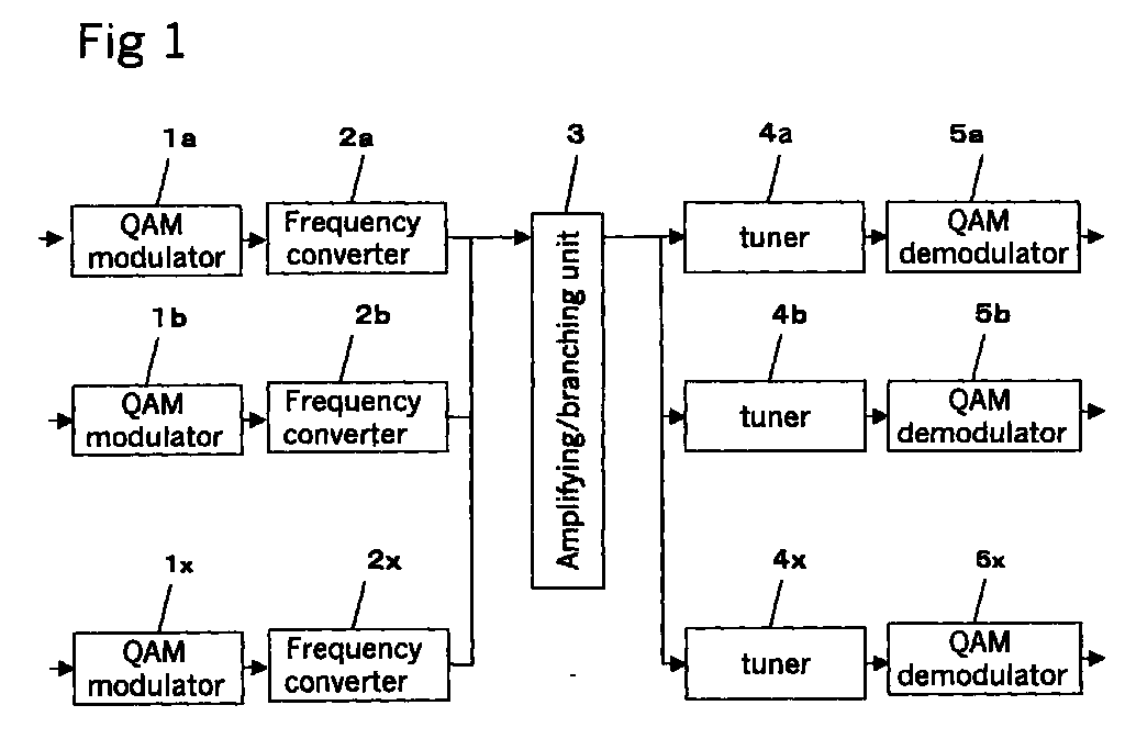
- Fig. 1 shows the configuration of a transmitting and receiving apparatus of Embodiment 1 of the invention.
- 1a to 1x denote QAM modulators
- 2a to 2x denote frequency converters
- 3 denotes an amplifying/branching unit
- 4a to 4x denote tuners
- 5a to 5x denote QAM demodulators.
- MPEG transport streams TSa to TSx of a rate of 41.34 Mbps are input to the QAM modulators 1a to 1x, respectively.
- An MPEG transport stream is a data string which is considered to be used in communication, has enhanced resistance to a transmission error and a program multiplexing function, and is used in the unit of a fixed-length packet of 188 bytes.
- the structure of such a packet is described in detail in, for example, "MPEG SYSTEM FOR MULTIPLYING MULTIMEDIA" at page 231 of "SAISIN MPEG KYOKASHO" (1994, ASCII SHUPPANKYOKU).
- Each of the QAM modulators 1a to 1x outputs a 64-QAM modulated wave of a center frequency of 36.125 MHz.
- the signals output from the QAM modulators 1a to 1x are input to the frequency converters 2a to 2x, respectively.
- Each of the frequency converters 2a to 2x has an internal PLL frequency synthesizer, and outputs a signal in which the center frequency of the input signal is converted.
- the frequency converter 2a outputs a signal of 141 MHz
- the frequency converter 2b outputs a signal of 149 MHz
- the frequency converter 2x outputs a signal of 325 MHz. All the output signals are arranged at intervals of 8 MHz so as not overlap with one another on the frequency axis.
- the signals output from the frequency converters 2a to 2x are input to the amplifying/branching unit 3.
- the amplifying/branching unit 3 amplifies and branches the input signals, and outputs the amplified and branched signals.
- the signals output from the amplifying/branching unit 3 are input to the tuners 4a to 4x.
- Each of the tuners 4a to 4x has an internal PLL frequency synthesizer, selects one of the input signals, and converts the center frequency to 36.125 MHz.
- the tuner 4a selects the signal of 141 MHZ
- the tuner 4b selects the signal of 149 MHz
- the tuner 4x selects the signal of 325 MHz.
- the tuners convert the frequencies of the selected signals to 36.125 MHz.
- the signals output from the tuners 4a to 4x are input to the QAM demodulators 5a to 5x, respectively.
- Each of the QAM demodulators 5a to 5x demodulates the input signal and outputs a reproduced data of a rate of 41.34 Mbps.
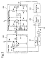
- Fig. 2 shows the configuration of the PLL frequency synthesizer included in each of the frequency converters 2a to 2x and the tuners 4a to 4x.
- 21 denotes a PLL synthesizer IC
- 22 denotes a loop filter
- 23 denotes a voltage controlled oscillator
- 24 denotes an amplifying IC
- 25 denotes a branch coil
- R1 to R10 denote resistors
- C1 to C11 denote capacitors
- L denotes a coil
- Tr1 to Tr3 denote transistors
- X denotes a crystal oscillator.
- a signal output from the PLL synthesizer IC 21 is input to the loop filter 22.
- the loop filter 22 is configured by: a first integration section consisting of the capacitors C1 and C2 and the resistor R1; a voltage level shift section consisting of the resistor R2 and a transistor Tr1; and a second integration section consisting of the resistor R3 and the capacitor C3.
- the loop filter 22 performs smoothing of the signal output from the PLL synthesizer IC 21, and a level shift based on a DC voltage Vb.
- a signal output from the loop filter 22 is input to the voltage controlled oscillator 23 via the resistor R4.
- the voltage controlled oscillator 23 is configured by: an oscillation section consisting of the resistors R5 to R7, the capacitors C4 to C6, a variable capacitor Cv, the coil L, and the transistor Tr2; and a buffer section consisting of the resistors R8 to R10 and the transistor Tr3.
- the capacitance of the variable capacitor Cv is changed in accordance with the voltage level of the signal output from the loop filter 22, and a signal of a frequency corresponding to the change of the capacitance is output.
- the signal output from the voltage controlled oscillator 23 is input to the amplifying IC 24 via the capacitor C8.
- the amplifying IC 24 amplifies the input signal by a constant factor.
- a signal output from the amplifying IC 24 is input to the branch coil 25.
- the branch coil 25 branches the signal output from the amplifying IC 24 into two signal portions. One of the signal portions is output to the PLL synthesizer IC 21 via the capacitor C9, and the other signal portion is output as an output signal Vo of the PLL frequency synthesizer via the capacitor C10.
- Fig. 3 shows the configuration of a carrier recovery section included in each of the QAM demodulators.
- 31 denotes an A/D conversion section
- 32 denotes a quadrature detection section
- 33 denotes a modulating component removal section
- 34 denotes a digital filter section
- 35 denotes an oscillation section.
- the A/D conversion section 31 converts an analog signal input to the corresponding QAM demodulator into a digital signal.
- a data output from the A/D conversion section 31 is input to the quadrature detection section 32.
- the quadrature detection section 32 performs quadrature detection on the data output from the A/D conversion section 31, by using a data output from the oscillation section 35, to produce I- and Q-axis data.
- the two data output from the quadrature detection section 32 are input to the modulating component removal section 33.
- the modulating component removal section 33 removes modulating components from the I- and Q-axis data to produce carrier components.
- a data output from the modulating component removal section 33 is input to the digital filter section 34.
- the digital filter section 34 has a frequency characteristic of allowing only a signal of a low frequency region to pass therethrough, and smoothes the input data to remove noise components.
- a data output from the digital filter section 34 is input to the oscillation section 35.
- the oscillation section 35 produces sinusoidal and cosinusoidal wave data from the input data.
- the sinusoidal and cosinusoidal wave data output from the oscillation section 35 coincide with the carrier components contained in the QAM modulated wave input to the A/D conversion section 31.
- vibrations which are applied to a transmitting and receiving apparatus in an airplane are variously changed in accordance with the flying state of the airplane, such as the weather and the altitude, and the place in the airplane where the apparatus is disposed. According to standards for vibration resistance tests on the ground, such vibrations have a frequency in the range of 10 Hz to 2 kHz. This is described in, for example, “Vibration" of Section 8 of "DO-160D/Environmental Condition and Test Procedures for Airborne Equipment” (1997, RTCA).
- Embodiment 1 of the invention data errors due to such mechanical vibrations are prevented from occurring in the QAM demodulators, in the following manner.
- the natural angular frequency ⁇ 0 is set to be in the vicinity of the maximum frequency of 2 kHz of mechanical vibrations.
- the natural angular frequency ⁇ 0 is expressed by the following expressions by using the resistor R1, the capacitors C1 and C2, the gain Kd of a phase comparator 21 , the gain Ko of the voltage controlled oscillator 23, the frequency division ratio P of a prescaler divider in the phase comparator 21 , the frequency division ratio N of a programmable divider in the phase comparator 21 , and a damping factor ⁇ .
- C1 Kd ⁇ Ko/(P ⁇ N ⁇ ⁇ 0 2 )
- R1' 2 ⁇ ⁇ /( ⁇ 0 ⁇ C1)
- R1' (1 + c2/c1) ⁇
- R1 C2 C1/C5
- R1' 3.9 k ⁇
- C1 47 nF
- C2 12 nF
- Kd 150 uA/2 ⁇
- Ko 15 MHz/V
- ⁇ 0.8.
- the natural angular frequency is set to about 8 krad/sec (about 1.3 kHz).
- the crystal oscillator X of 4 MHz is externally connected to the PLL synthesizer IC, and the phase comparison sampling frequency is set to 1 MHz.
- Fig. 10 shows a state of occurrence of a data error with respect to the natural angular frequency ⁇ 0.
- the mark ⁇ indicates a case where, even when mechanical vibrations are applied, a resulting data error of the QAM demodulator is allowable, and the mark x indicates a case where a resulting data error is not allowable.
- the natural angular frequency is set to be in the vicinity of the maximum frequency of 2 kHz of mechanical vibrations as described above, it is seen that, even when the characteristics of the capacitors and coils included in the loop filter 22 and the voltage controlled oscillator 23 are changed by the mechanical vibrations in the range of 10 Hz to 2 kHz, the PLL frequency synthesizers and the carrier recovery sections can rapidly follow changes to suppress generation of noises.
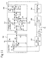
- Fig. 11 shows the configuration of another PLL frequency synthesizer.
- 21 denotes a PLL synthesizer IC
- 22 denotes a loop filter
- 26 denotes a voltage controlled oscillator
- 24 denotes an amplifying IC
- 25 denotes a branch coil
- R1 to R6 denote resistors
- C1 to C15 denote capacitors
- LC denotes a resonance circuit
- Tr1 to Tr3 denote transistors
- X denotes a crystal oscillator.
- the PLL frequency synthesizers and the carrier recovery sections can rapidly follow changes to suppress generation of noises.
- the setting to the vicinity of 2 kHz means a range of ⁇ 50% with respect the maximum frequency.
- the loop bandwidth is set to be sufficiently higher than 2 kHz which is the maximum frequency of mechanical vibrations.
- the loop bandwidth is determined by the configuration and the operating frequency of the digital filter 34. This is described by WILLIAM et al. in, for example, p. 426 of "A Survey of Digital Phase-Locked Loops” (1981, Proceeding of the IEEE, vol. 69, No. 4).
- the digital filter 34 is configured to be of the secondary type, and the operating rate is set to an integer multiple of the symbol rate, so that the loop bandwidth is set to about 15 kHz.
- Fig. 12 is a diagram showing a state of occurrence of a data error with respect to the loop bandwidth.
- the mark ⁇ indicates a case where, even when mechanical vibrations are applied, a resulting data error of the QAM demodulator is allowable, and the mark x indicates a case where a resulting data error is not allowable.
- the carrier recovery sections can rapidly follow changes to prevent a data error from being generated.
- the sufficiently higher setting means that the loop bandwidth is higher than the maximum frequency by at least 5 kHz.
- the transmitting and receiving apparatus comprising: the QAM modulators 1a to 1x which modulate an input digital data; the frequency converters 2a to 2x which convert signals respectively output from the QAM modulators 1a to 1x into signals of predetermined frequencies; the amplifying/branching unit 3 which amplifies and branches signals output from the frequency converters 2a to 2x; the tuners 4a to 4x which respectively convert signals output from the amplifying/branching unit 3, into signals of a predetermined frequency; and the QAM demodulators 5a to 5x which demodulate digital data from signals output from the tuners 4a to 4x, each of the frequency converters 2a to 2x and the tuners 4a to 4x comprises a PLL frequency synthesizer, each of the QAM demodulators 5a to 5x comprises a carrier recovery section, the natural angular frequencies of the PLL frequency synthesizers are set to be in the vicinity of the maximum frequency of mechanical vibrations which are externally applied, and the loop
- Embodiment 2 of the invention is identical with Embodiment 1 except that the coil L used in the resonance section of the voltage controlled oscillator 23 included in the PLL frequency synthesizer of Fig. 2 is configured by a microstrip line, and hence description of its operation is omitted.
- the coil L configured by the microstrip line will be described.
- the coil L exerts the largest influence on the oscillation frequency fvco. Therefore, the coil L is configured by a microstrip line in which the characteristics are less changed by mechanical vibrations.
- the coil L is configured to be of the air core type, its shape is easily changed by mechanical vibrations, and hence the characteristics are largely changed.
- the inductance of a microstrip line is described in, for example, page 172 of "MICROWAVE KAIRO NO KISO TO SONO OYO" (1990, SOGO DENSHI SHUPPANSHA).
- Embodiment 3 of the invention is identical with Embodiment 1 except that the coil L used in the resonance section of the voltage controlled oscillator 23 included in the PLL frequency synthesizer of Fig. 2 is configured by a microstrip line and a reinforcing plate is pasted to the upper side of the microstrip line, and hence description of its operation is omitted.
- the configuration of the microstrip line will be described.
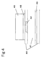
- Fig. 4 is a section view of the microstrip line and showing Embodiment 3 of the invention.
- 41 denotes a printed circuit board
- 42 denotes the microstrip line
- 43 denotes a grounding conductor
- 44 denotes a sheathing resin.
- the reinforcing plate 45 is pasted to the upper side of the microstrip line 42.
- the reinforcing plate 45 is a board which is made of the same material as the printed circuit board 41.
- the adhesive agent 46 used is an epoxy or silicone adhesive agent having excellent insulating properties, or a double-coated adhesive tape having excellent insulating properties.
- the reinforcing plate 45 functions as a reinforcing member against mechanical shocks and vibrations, and hence the change in characteristics of the microstrip line can be suppressed.
- Embodiment 4 of the invention is identical with Embodiment 1 except that the coil L used in the resonance section of the voltage controlled oscillator 23 included in the PLL frequency synthesizer of Fig. 2 is configured to be of the chip surface mount type, and hence description of its operation is omitted.
- the coil L which is configured to be of the chip surface mount type will be described.
- Fig. 9 is a section view of a vicinity of a coil of the chip surface mount type and showing Embodiment 4 of the invention.
- 91 denotes a printed circuit board
- 92 denotes a conductor pattern
- 93 denotes a sheathing resin
- 94 denotes a chip surface mount type coil
- 95 denotes solder.
- the conductor pattern 92 formed on the printed circuit board 91 is covered with the sheathing resin 93 except a portion to which the chip surface mount type coil 94 is to be soldered.
- the coil L is configured by a coil of the chip surface mount type in which a less stress is produced by mechanical vibrations.
- the coil L is configured to be of the air core type, its shape is easily changed by mechanical vibrations, and hence the characteristics are largely changed.
- a chip surface mount type coil is substantially equal in size to a chip type capacitor or resistor, and a mechanical stress is hardly transmitted from a printed circuit board to the coil.
- Embodiment 5 of the invention is identical with Embodiment 1 except that the coil L used in the resonance section of the voltage controlled oscillator 23 included in the PLL frequency synthesizer of Fig. 2 is configured by a microstrip line and the microstrip line is formed by an inner layer of a printed circuit board, and hence description of its operation is omitted.
- the configuration of the microstrip line will be described.
- Fig. 5 is a section view of the microstrip line and showing Embodiment 5 of the invention.
- 51 denotes the printed circuit board
- 52 denotes the microstrip line
- 53 denotes a grounding conductor
- 54 denotes a sheathing resin
- 55 denotes a shield cover.
- the microstrip line 52 is different from a prior art one in that the microstrip line is formed inside the printed circuit board.
- the shield cover 55 is attached to the printed circuit board 51.
- the microstrip line 52 is formed in an outer layer of the printed circuit board 51, severe mechanical shocks and vibrations in an airplane cause spatial conditions with respect to the shield cover 55 to be varied, and hence characteristics of the microstrip line are changed.
- This change in characteristics causes the oscillation frequency fvco of the voltage controlled oscillator 23 to be varied.
- noise components contained in the output signals of the PLL frequency synthesizers are increased, and therefore the QAM demodulators 5a to 5x output erroneous reproduced data.
- the microstrip line 52 is formed in an internal layer of the printed circuit board 51, so that the microstrip line 52 is not directly opposed to the shield cover 55 attached to the printed circuit board 51. According to this configuration, a part of the printed circuit board 51 is interposed between the microstrip line 52 and the shield cover 55, and hence variations of spatial conditions due to mechanical shocks and vibrations can be reduced.
- Embodiment 6 of the invention is identical with Embodiment 1 except that the capacitors C1, C2, and C3 used in the loop filter 22, and the capacitors C4, C5, and C6 used in the resonance section of the voltage controlled oscillator 23 which are included in the PLL frequency synthesizer of Fig. 2 are configured to be of the film type, and hence description of its operation is omitted.
- the capacitors of the film type will be described.
- the loop filter 22 is configured by: the first integration section consisting of the capacitors C1 and C2 and the resistor R1; the voltage level shift section consisting of the resistor R2 and the transistor Tr1; and the second integration section consisting of the resistor R3 and the capacitor C3, and performs smoothing of the signal output from the PLL synthesizer IC 21, and a level shift based on the DC voltage Vb.
- the capacitors C1 to C3 capacitors of the ceramic type are used in view of the high-frequency characteristics and size.
- the voltage controlled oscillator 23 is configured by: the oscillation section consisting of the resistors R5 to R7, the capacitors C4 to C6, the variable capacitor Cv, the coil L, and the transistor Tr2; and the buffer section consisting of the resistors R8 to R10 and the transistor Tr3.
- the oscillator outputs the signal of the oscillation frequency fvco indicated by Expressions 5 and 6.
- capacitors C1 to C6 capacitors of the ceramic type are used in view of the high-frequency characteristics and size.
- a capacitor of the ceramic type has a drawback that, as compared with one of the film type, the piezoelectric effect is large and easily affected by mechanical shocks and vibrations.
- the capacitors C1 to C3 used in the loop filter 22, and the capacitors C4 to C6 used in the resonance section of the voltage controlled oscillator 23 are configured to be of the film type.
- a capacitor of the film type is excellent all in high-frequency, temperature, and vibration resistance characteristics.
- capacitors C1 to C3 used in the loop filter 22, and the capacitors C4 to C6 used in the resonance section of the voltage controlled oscillator 23 are configured to be of the film type as described above, characteristic changes due to mechanical shocks and vibrations can be reduced to suppress frequency variations of the voltage controlled oscillator 23.
- Embodiment 7 of the invention is identical with Embodiment 3 except that a rubber member is pasted to the upper side of the reinforcing plate of Fig. 4, and hence description of its operation is omitted.
- the rubber member will be described.
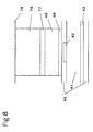
- Fig. 8 is a section view of the microstrip line and showing Embodiment 7 of the invention.
- 41 denotes the printed circuit board
- 42 denotes the microstrip line
- 43 denotes the grounding conductor
- 44 denotes the sheathing resin
- 45 denotes the reinforcing plate
- 46 denotes the adhesive agent.
- the embodiment is different from Embodiment 3 in that an adhesive agent 77 is applied to the upper side of the reinforcing plate 45 and a rubber member 79 is inserted between the reinforcing plate and a shield cover 78.
- the shield cover 78 is attached to the printed circuit board 41.
- the shield cover 78 When severe mechanical shocks and vibrations in an airplane are applied to the printed circuit board 41, the shield cover 78 resonates, and characteristics of the microstrip line and the capacitors which are covered by the cover are changed. This change in characteristics increases noise components contained in the output signals of the PLL frequency synthesizers, and the QAM demodulators 5a to 5x output erroneous reproduced data.
- the rubber member 79 is inserted between the reinforcing plate 45 and the shield cover 78 by using the adhesive agent 77. According to this configuration, the rubber member 79 functions as a member for absorbing mechanical shocks and vibrations, so as to prevent the shield cover 78 from resonating, whereby the change in characteristics of the microstrip line and the capacitors can be suppressed.
- the numbers of the QAM modulators, the frequency converters, the tuners, and the QAM demodulators are a to x or 24.
- the numbers may not be 24, and the numbers of the QAM modulators and the frequency converters may not be equal to those of the tuners and the QAM demodulators.
- the MPEG transport streams of a rate of 41.34 Mbps are input to the QAM modulators 1a to 1x, and the modulators output 64-QAM modulated waves of a center frequency of 36.125 MHz.
- the rate of the MPEG transport streams, and the center frequency and modulation method of the output signals are not restricted to the above.
- the frequency converter 2a outputs the signal of 141 MHz
- the frequency converter 2b outputs the signal of 149 MHz
- the frequency converter 2x outputs the signal of 325 MHz.
- signals of other frequencies may be output as far as all the signals do not overlap with each other on the frequency axis.
- the tuner 4a selects the signal of 141 MHz
- the tuner 4b selects the signal of 149 MHz
- the tuner 4x selects the signal of 325 MHz
- the tuners then perform frequency conversion to 36.125 MHz.
- the signals to be selected, and the frequency of the frequency conversion are not restricted to the above as far as the tuners can operate.
- each PLL frequency synthesizer is set to about 8 krad/sec.
- the natural angular frequency may be set to another value as far as the value is in the vicinity of the maximum frequency of mechanical vibrations.
- the phase comparison frequency of each PLL frequency synthesizer is set to 1 MHz.
- the frequency may have another value as far as the natural angular frequency is in the vicinity of the maximum frequency of mechanical vibrations.
- the digital filter 34 of the carrier recovery section is configured to be of the secondary type, and the operating rate is set to an integer multiple of the symbol rate, and the loop bandwidth is set to about 15 kHz.
- Other configuration and value may be employed as far as the frequency is higher than the maximum frequency of mechanical vibrations.
- the reinforcing plate 45 is pasted to the upper side of the microstrip line 42. Alternatively, the reinforcing plate 45 may be pasted to the lower side or both the sides of the microstrip line. In Embodiment 3, the reinforcing plate 45 is made of the same material as the printed circuit board 41. Alternatively, the reinforcing plate may be made of a different material as far as characteristics of the microstrip line is adversely affected. In Embodiment 3, an epoxy or silicone adhesive agent having excellent insulating properties is used as the adhesive agent 46. The adhesive agent may consists of other components as far as characteristics of the microstrip line is adversely affected.
- the capacitors C1 to C3 used in the loop filter 22, and the capacitors C4 to C6 used in the resonance section of the voltage controlled oscillator 23 which are included in the PLL frequency synthesizers are of the film type. Alternatively, only a part of the capacitors may be of the film type.
Landscapes
- Engineering & Computer Science (AREA)
- Signal Processing (AREA)
- Computer Networks & Wireless Communication (AREA)
- Stabilization Of Oscillater, Synchronisation, Frequency Synthesizers (AREA)
- Digital Transmission Methods That Use Modulated Carrier Waves (AREA)
- Superheterodyne Receivers (AREA)
- Transmitters (AREA)
- Transceivers (AREA)
Abstract
Description
modulating means for modulating an input digital data; first frequency converting means for converting a signal output from said modulating means into a signal of a predetermined frequency; amplifying/branching means for amplifying and branching a signal output from said first frequency converting means; second frequency converting means for converting a signal output from said amplifying/branching means, into a signal of a predetermined frequency; and demodulating means for demodulating a digital data from a signal output from said second frequency converting means, wherein
Claims (11)
- A transmitting and receiving apparatus comprising: modulating means for modulating an input digital data; first frequency converting means for converting a signal output from said modulating means into a signal of a predetermined frequency; amplifying/branching means for amplifying and branching a signal output from said first frequency converting means; second frequency converting means for converting a signal output from said amplifying/branching means, into a signal of a predetermined frequency; and demodulating means for demodulating a digital data from a signal output from said second frequency converting means, whereineach of said first and second frequency converting means comprises a PLL frequency synthesizer,said demodulating means has a carrier recovery section, andnatural angular frequencies of said PLL frequency synthesizers are set to be equal to a maximum frequency of mechanical vibrations which are externally applied, or in a predetermined width above and below the maximum frequency, ora loop filter bandwidth of said carrier recovery section is set to be higher by a predetermined amount than the maximum frequency of mechanical vibrations which are externally applied.
- A transmitting and receiving apparatus according to claim 1, wherein the predetermined width is a range of ±50 % above and below with respect the maximum frequency, and the predetermined amount is 5 kHz.
- A transmitting and receiving apparatus according to claim 1 or 2, wherein each of said PLL frequency synthesizers has:a PLL synthesizer IC to which a crystal oscillator is externally connected; a loop filter which filters a signal output from said PLL synthesizer IC; a voltage controlled oscillator in which an oscillation frequency is changed in accordance with a signal output from said loop filter; an amplifying IC which amplifies a signal output from said voltage controlled oscillator; and a branch coil which branches a signal output from said amplifying IC, andone of signals output from said branch coil is input to said PLL synthesizer IC.
- A transmitting and receiving apparatus according to claim 1 or 2, wherein said carrier recovery section has:an A/D conversion section which converts an input analog signal into a digital signal; a quadrature detection section which performs quadrature calculation on a data output from said A/D conversion section; a modulating component removal section which removes modulating components from a data output from said quadrature detection section; a digital filter section which filters a data output from said modulating component removal section; and an oscillation section in which an oscillation frequency is changed in accordance with a data output from said digital filter section, andeach of said oscillation section and said A/D conversion section input a data to said quadrature detection section.
- A transmitting and receiving apparatus according to claim 1 or 2, wherein a phase comparison frequency of a PLL synthesizer IC included in said PLL frequency synthesizer is set to be higher than the maximum frequency of mechanical vibrations which are externally applied.
- A transmitting and receiving apparatus comprising: modulating means for modulating an input digital data; first frequency converting means for converting a signal output from said modulating means into a signal of a predetermined frequency; amplifying/branching means for amplifying and branching a signal output from said first frequency converting means; second frequency converting means for converting a signal output from said amplifying/branching means, into a signal of a predetermined frequency; and demodulating means for demodulating a digital data from a signal output from said second frequency converting means, whereineach of said first and second frequency converting means comprises a PLL frequency synthesizer,said demodulating means has a carrier recovery section, anda coil used in an oscillation section of a voltage controlled oscillator included in each of said PLL frequency synthesizers is a microstrip line.
- A transmitting and receiving apparatus comprising: modulating means for modulating an input digital data; first frequency converting means for converting a signal output from said modulating means into a signal of a predetermined frequency; amplifying/branching means for amplifying and branching a signal output from said first frequency converting means; second frequency converting means for converting a signal output from said amplifying/branching means, into a signal of a predetermined frequency; and demodulating means for demodulating a digital data from a signal output from said second frequency converting means, whereineach of said first and second frequency converting means comprises a PLL frequency synthesizer,said demodulating means has a carrier recovery section, anda reinforcing plate is pasted to an upper side and/or a lower side of a microstrip line used in an oscillation section of a voltage controlled oscillator included in each of said PLL frequency synthesizers.
- A transmitting and receiving apparatus comprising: modulating means for modulating an input digital data; first frequency converting means for converting a signal output from said modulating means into a signal of a predetermined frequency; amplifying/branching means for amplifying and branching a signal output from said first frequency converting means; second frequency converting means for converting a signal output from said amplifying/branching means, into a signal of a predetermined frequency; and demodulating means for demodulating a digital data from a signal output from said second frequency converting means, whereineach of said first and second frequency converting means comprises a PLL frequency synthesizer,said demodulating means has a carrier recovery section, anda coil used in an oscillation section of a voltage controlled oscillator included in each of said PLL frequency synthesizers is of a chip surface mount type.
- A transmitting and receiving apparatus comprising: modulating means for modulating an input digital data; first frequency converting means for converting a signal output from said modulating means into a signal of a predetermined frequency; amplifying/branching means for amplifying and branching a signal output from said first frequency converting means; second frequency converting means for converting a signal output from said amplifying/branching means, into a signal of a predetermined frequency; and demodulating means for demodulating a digital data from a signal output from said second frequency converting means, whereineach of said first and second frequency converting means comprises a PLL frequency synthesizer,said demodulating means has a carrier recovery section, anda microstrip line used in an oscillation section of a voltage controlled oscillator included in each of said PLL frequency synthesizers is formed by an inner layer of a printed circuit board.
- A transmitting and receiving apparatus comprising: modulating means for modulating an input digital data; first frequency converting means for converting a signal output from said modulating means into a signal of a predetermined frequency; amplifying/branching means for amplifying and branching a signal output from said first frequency converting means; second frequency converting means for converting a signal output from said amplifying/branching means, into a signal of a predetermined frequency; and demodulating means for demodulating a digital data from a signal output from said second frequency converting means, whereineach of said first and second frequency converting means comprises a PLL frequency synthesizer,said demodulating means has a carrier recovery section, andcapacitors used in a loop filter and a voltage controlled oscillator included in each of said PLL frequency synthesizers are of a film type.
- A transmitting and receiving apparatus comprising: modulating means for modulating an input digital data; first frequency converting means for converting a signal output from said modulating means into a signal of a predetermined frequency; amplifying/branching means for amplifying and branching a signal output from said first frequency converting means; second frequency converting means for converting a signal output from said amplifying/branching means, into a signal of a predetermined frequency; and demodulating means for demodulating a digital data from a signal output from said second frequency converting means, whereineach of said first and second frequency converting means comprises a PLL frequency synthesizer,said demodulating means has a carrier recovery section, anda reinforcing plate is pasted to an upper side and/or a lower side of a microstrip line used in an oscillation section of a voltage controlled oscillator included in each of said PLL frequency synthesizers, and a rubber member is inserted between said reinforcing plate and an outer shield cover.
Applications Claiming Priority (2)
| Application Number | Priority Date | Filing Date | Title |
|---|---|---|---|
| JP1060099 | 1999-01-19 | ||
| JP01060099A JP3492225B2 (en) | 1999-01-19 | 1999-01-19 | Transceiver |
Publications (3)
| Publication Number | Publication Date |
|---|---|
| EP1022856A2 true EP1022856A2 (en) | 2000-07-26 |
| EP1022856A3 EP1022856A3 (en) | 2003-04-16 |
| EP1022856B1 EP1022856B1 (en) | 2004-04-28 |
Family
ID=11754749
Family Applications (1)
| Application Number | Title | Priority Date | Filing Date |
|---|---|---|---|
| EP00100929A Expired - Lifetime EP1022856B1 (en) | 1999-01-19 | 2000-01-18 | Transmitting and receiving apparatus capable of the suppression of the microphonic noise in digital transmission system |
Country Status (4)
| Country | Link |
|---|---|
| US (2) | US6859502B1 (en) |
| EP (1) | EP1022856B1 (en) |
| JP (1) | JP3492225B2 (en) |
| DE (1) | DE60010134T2 (en) |
Cited By (2)
| Publication number | Priority date | Publication date | Assignee | Title |
|---|---|---|---|---|
| CN103312344A (en) * | 2012-03-06 | 2013-09-18 | 索尼公司 | Data receiving circuit, data transmitting circuit, data transmitting and receiving device, data transmission system, and data receiving method |
| US9160347B1 (en) | 2014-08-07 | 2015-10-13 | Symbol Technologies, Llc | System and method for countering the effects of microphonics in a phase locked loop |
Families Citing this family (5)
| Publication number | Priority date | Publication date | Assignee | Title |
|---|---|---|---|---|
| JP3461745B2 (en) | 1999-02-16 | 2003-10-27 | 三菱電機株式会社 | Communication device |
| JP2002077084A (en) | 2000-09-04 | 2002-03-15 | Matsushita Electric Ind Co Ltd | Signal distribution system, transmitting device, receiving device, medium, and information aggregate |
| CN1989751B (en) * | 2004-07-15 | 2011-07-13 | 汤姆森特许公司 | System and method for improved carrier recovery |
| US20100252631A1 (en) * | 2009-04-01 | 2010-10-07 | Infineon Technologies Ag | High speed contactless communication |
| US8369433B2 (en) | 2010-01-08 | 2013-02-05 | Broadcom Corporation | Digital up-converter and N-channel modulator with flexible association of QAM generation resources to narrowcast and broadcast frequencies |
Family Cites Families (35)
| Publication number | Priority date | Publication date | Assignee | Title |
|---|---|---|---|---|
| US4079329A (en) | 1976-11-11 | 1978-03-14 | Harris Corporation | Signal demodulator including data normalization |
| DE2803846C2 (en) * | 1977-01-31 | 1986-01-30 | Hitachi, Ltd., Tokio/Tokyo | Centimeter wave oscillator circuit with a field effect transistor |
| JPS56717A (en) * | 1979-06-15 | 1981-01-07 | Nissan Motor Co Ltd | Radar unit with shield cover |
| JPS58161504A (en) * | 1982-03-19 | 1983-09-26 | Nec Corp | Voltage control oscillator |
| JPS6248102A (en) * | 1985-08-27 | 1987-03-02 | Matsushita Electric Works Ltd | Microstrip line antenna |
| FR2614151A1 (en) * | 1987-04-15 | 1988-10-21 | Alcatel Thomson Faisceaux | HYPERFREQUENCY OSCILLATOR WITH DIELECTRIC RESONATOR, PARTICULARLY IN THE RANGE OF 22 GHZ |
| JP2855628B2 (en) | 1988-05-11 | 1999-02-10 | セイコーエプソン株式会社 | Phase locked loop |
| JPH02296425A (en) | 1989-05-10 | 1990-12-07 | Nec Eng Ltd | Phase comparison system for middle wave synchronizing broadcast |
| JPH03174816A (en) * | 1989-12-02 | 1991-07-30 | Toshiba Corp | Pll circuit |
| JPH03278701A (en) * | 1990-03-28 | 1991-12-10 | Tdk Corp | High frequency amplifier |
| JP3402369B2 (en) | 1991-11-11 | 2003-05-06 | ティーディーケイ株式会社 | Oscillator module |
| EP0519085B1 (en) | 1990-12-26 | 1996-10-16 | TDK Corporation | High-frequency device |
| US5289272A (en) * | 1992-02-18 | 1994-02-22 | Hughes Aircraft Company | Combined data, audio and video distribution system in passenger aircraft |
| US5528633A (en) * | 1992-03-13 | 1996-06-18 | Comstream Corporation | Tuner with quadrature downconverter for pulse amplitude modulated data applications |
| WO1993020615A1 (en) * | 1992-04-03 | 1993-10-14 | SIEMENS AKTIENGESELLSCHAFT öSTERREICH | 1.6 TO 3 GHz OSCILLATOR |
| US5574570A (en) * | 1992-05-12 | 1996-11-12 | Mitsubishi Denki Kabushiki Kaisha | Video signal recording/reproduction apparatus and method for recording/reproducing two kinds of video signals carrying different amounts of information |
| JPH0685700A (en) | 1992-09-02 | 1994-03-25 | Matsushita Electric Ind Co Ltd | PLL frequency synthesizer tuner |
| JP3223003B2 (en) | 1993-09-20 | 2001-10-29 | 三洋電機株式会社 | Multiplex circuit |
| JP2715873B2 (en) | 1993-12-24 | 1998-02-18 | 日本電気株式会社 | Slot synchronization method |
| US5600365A (en) | 1994-01-28 | 1997-02-04 | Sony Corporation | Multiple audio and video signal providing apparatus |
| JPH07255043A (en) | 1994-01-28 | 1995-10-03 | Sony Corp | Information provision device |
| US5402087A (en) * | 1994-04-08 | 1995-03-28 | B.E.L.-Tronics Limited | Voltage controlled push-push oscillator |
| JP3461905B2 (en) | 1994-04-15 | 2003-10-27 | 株式会社東芝 | Digital transmission signal receiving circuit |
| JPH0879069A (en) * | 1994-09-08 | 1996-03-22 | Mitsubishi Electric Corp | VCO circuit and PLL circuit |
| JPH08331057A (en) * | 1995-03-27 | 1996-12-13 | Sony Corp | Optical signal transmitter, optical signal receiver, and optical signal transmitter / receiver |
| US6320842B1 (en) * | 1996-02-01 | 2001-11-20 | Canon Kabushiki Kaisha | Spread spectrum communication apparatus |
| JPH09219576A (en) | 1996-02-13 | 1997-08-19 | Sumitomo Electric Ind Ltd | Chip capacitor mounting method |
| JP3381580B2 (en) | 1996-11-22 | 2003-03-04 | 株式会社豊田中央研究所 | Adaptive communication device |
| US5970386A (en) * | 1997-01-27 | 1999-10-19 | Hughes Electronics Corporation | Transmodulated broadcast delivery system for use in multiple dwelling units |
| JPH10215119A (en) | 1997-01-29 | 1998-08-11 | Tdk Corp | Voltage controlled oscillator |
| JPH10285021A (en) | 1997-03-31 | 1998-10-23 | Toyo Commun Equip Co Ltd | Clock recovery circuit |
| US5942950A (en) * | 1997-05-12 | 1999-08-24 | Ail Systems, Inc. | Varactor tuned strip line resonator and VCO using same |
| JP3328548B2 (en) * | 1997-06-23 | 2002-09-24 | 小橋工業株式会社 | Method of fixing elastic plate to prevent soil adhesion of rotary work machine |
| IT1292213B1 (en) * | 1997-06-27 | 1999-01-25 | Italtel Spa | MICROWAVE VCO MADE IN PLANAR TECHNIQUE ON A SUBSTRATE WITH HIGH DIELECTRIC LOSSES |
| JPH11234128A (en) * | 1998-02-13 | 1999-08-27 | Matsushita Electric Ind Co Ltd | Oscillation circuit system, modulation system, demodulation system and multi-level QAM modulation / demodulation system |
-
1999
- 1999-01-19 JP JP01060099A patent/JP3492225B2/en not_active Expired - Lifetime
-
2000
- 2000-01-18 US US09/484,441 patent/US6859502B1/en not_active Expired - Lifetime
- 2000-01-18 DE DE60010134T patent/DE60010134T2/en not_active Expired - Lifetime
- 2000-01-18 EP EP00100929A patent/EP1022856B1/en not_active Expired - Lifetime
-
2005
- 2005-01-06 US US11/029,348 patent/US7206371B2/en not_active Expired - Lifetime
Cited By (3)
| Publication number | Priority date | Publication date | Assignee | Title |
|---|---|---|---|---|
| CN103312344A (en) * | 2012-03-06 | 2013-09-18 | 索尼公司 | Data receiving circuit, data transmitting circuit, data transmitting and receiving device, data transmission system, and data receiving method |
| CN103312344B (en) * | 2012-03-06 | 2017-03-01 | 索尼公司 | Data receiver, transtation mission circuit and equipment, data transmission system and method for reseptance |
| US9160347B1 (en) | 2014-08-07 | 2015-10-13 | Symbol Technologies, Llc | System and method for countering the effects of microphonics in a phase locked loop |
Also Published As
| Publication number | Publication date |
|---|---|
| DE60010134T2 (en) | 2004-08-26 |
| US6859502B1 (en) | 2005-02-22 |
| JP2000209086A (en) | 2000-07-28 |
| US7206371B2 (en) | 2007-04-17 |
| DE60010134D1 (en) | 2004-06-03 |
| EP1022856A3 (en) | 2003-04-16 |
| JP3492225B2 (en) | 2004-02-03 |
| US20050152462A1 (en) | 2005-07-14 |
| EP1022856B1 (en) | 2004-04-28 |
Similar Documents
| Publication | Publication Date | Title |
|---|---|---|
| EP1332548B1 (en) | Direct conversion tuner | |
| JP3444727B2 (en) | Digital satellite broadcasting receiver | |
| US6094236A (en) | Tuner circuit | |
| EP0911962B1 (en) | Cable modem tuner | |
| CN1097877C (en) | Tuner for digital satellite receiver | |
| US20020051461A1 (en) | Data transmission method and apparatus | |
| EP1022856B1 (en) | Transmitting and receiving apparatus capable of the suppression of the microphonic noise in digital transmission system | |
| FI70356B (en) | SYSTEM FOER BEHANDLING AV TELEVISIONSSIGNALER | |
| US20040207476A1 (en) | PLL circuit and television receiver having same and beat reducing method for television receiver | |
| US7233368B2 (en) | Down-converter | |
| US6788747B1 (en) | Receiver capable of receiving analog broadcast and digital broadcast and IC for the same | |
| JP3373431B2 (en) | Digital broadcast receiver | |
| US5648823A (en) | Circuit configuration for intermediate frequency demodulation and device for video signal processing including the circuit | |
| JP3529644B2 (en) | Tuner circuit of digital broadcast receiver | |
| JP2000307456A (en) | Tuner and duplexer | |
| KR100247832B1 (en) | A high frequency electronic device | |
| JPH11234128A (en) | Oscillation circuit system, modulation system, demodulation system and multi-level QAM modulation / demodulation system | |
| US20020191117A1 (en) | Frequency conversion circuit, demodulation circuit, and television receiving device | |
| KR100333789B1 (en) | High frequency module | |
| US20050190304A1 (en) | Radio frequency (RF) modulator with narrow bandpass filter | |
| JP3599948B2 (en) | TV tuner with built-in RF modulator | |
| KR100722738B1 (en) | Oscillator and Method for TDD in Wireless Communication System | |
| JP2000032361A (en) | Digital broadcast receiver | |
| JP2001024539A (en) | Receiver | |
| Rieger | Use of Nonstandard FM Subcarriers for Telemetry Systems |
Legal Events
| Date | Code | Title | Description |
|---|---|---|---|
| PUAI | Public reference made under article 153(3) epc to a published international application that has entered the european phase |
Free format text: ORIGINAL CODE: 0009012 |
|
| AK | Designated contracting states |
Kind code of ref document: A2 Designated state(s): DE FR GB |
|
| AX | Request for extension of the european patent |
Free format text: AL;LT;LV;MK;RO;SI |
|
| PUAL | Search report despatched |
Free format text: ORIGINAL CODE: 0009013 |
|
| RIC1 | Information provided on ipc code assigned before grant |
Ipc: 7H 03B 5/18 B Ipc: 7H 03L 7/099 B Ipc: 7H 03L 1/00 A |
|
| AK | Designated contracting states |
Designated state(s): DE FR GB |
|
| AX | Request for extension of the european patent |
Extension state: AL LT LV MK RO SI |
|
| 17P | Request for examination filed |
Effective date: 20030424 |
|
| 17Q | First examination report despatched |
Effective date: 20030729 |
|
| GRAP | Despatch of communication of intention to grant a patent |
Free format text: ORIGINAL CODE: EPIDOSNIGR1 |
|
| AKX | Designation fees paid |
Designated state(s): DE FR GB |
|
| GRAA | (expected) grant |
Free format text: ORIGINAL CODE: 0009210 |
|
| GRAS | Grant fee paid |
Free format text: ORIGINAL CODE: EPIDOSNIGR3 |
|
| AK | Designated contracting states |
Kind code of ref document: B1 Designated state(s): DE FR GB |
|
| REG | Reference to a national code |
Ref country code: GB Ref legal event code: FG4D |
|
| REF | Corresponds to: |
Ref document number: 60010134 Country of ref document: DE Date of ref document: 20040603 Kind code of ref document: P |
|
| ET | Fr: translation filed | ||
| PLBE | No opposition filed within time limit |
Free format text: ORIGINAL CODE: 0009261 |
|
| STAA | Information on the status of an ep patent application or granted ep patent |
Free format text: STATUS: NO OPPOSITION FILED WITHIN TIME LIMIT |
|
| 26N | No opposition filed |
Effective date: 20050131 |
|
| REG | Reference to a national code |
Ref country code: FR Ref legal event code: PLFP Year of fee payment: 17 |
|
| REG | Reference to a national code |
Ref country code: FR Ref legal event code: PLFP Year of fee payment: 18 |
|
| REG | Reference to a national code |
Ref country code: FR Ref legal event code: PLFP Year of fee payment: 19 |
|
| PGFP | Annual fee paid to national office [announced via postgrant information from national office to epo] |
Ref country code: FR Payment date: 20181213 Year of fee payment: 20 |
|
| PGFP | Annual fee paid to national office [announced via postgrant information from national office to epo] |
Ref country code: DE Payment date: 20190108 Year of fee payment: 20 Ref country code: GB Payment date: 20190116 Year of fee payment: 20 |
|
| REG | Reference to a national code |
Ref country code: DE Ref legal event code: R071 Ref document number: 60010134 Country of ref document: DE |
|
| REG | Reference to a national code |
Ref country code: GB Ref legal event code: PE20 Expiry date: 20200117 |
|
| PG25 | Lapsed in a contracting state [announced via postgrant information from national office to epo] |
Ref country code: GB Free format text: LAPSE BECAUSE OF EXPIRATION OF PROTECTION Effective date: 20200117 |