EP1021069A2 - Microwave oven with magnetic field sensor - Google Patents
Microwave oven with magnetic field sensor Download PDFInfo
- Publication number
- EP1021069A2 EP1021069A2 EP00300200A EP00300200A EP1021069A2 EP 1021069 A2 EP1021069 A2 EP 1021069A2 EP 00300200 A EP00300200 A EP 00300200A EP 00300200 A EP00300200 A EP 00300200A EP 1021069 A2 EP1021069 A2 EP 1021069A2
- Authority
- EP
- European Patent Office
- Prior art keywords
- waveguide
- microwave oven
- loop
- antenna sensor
- circuit board
- Prior art date
- Legal status (The legal status is an assumption and is not a legal conclusion. Google has not performed a legal analysis and makes no representation as to the accuracy of the status listed.)
- Granted
Links
Images


Classifications
-
- H—ELECTRICITY
- H05—ELECTRIC TECHNIQUES NOT OTHERWISE PROVIDED FOR
- H05B—ELECTRIC HEATING; ELECTRIC LIGHT SOURCES NOT OTHERWISE PROVIDED FOR; CIRCUIT ARRANGEMENTS FOR ELECTRIC LIGHT SOURCES, IN GENERAL
- H05B6/00—Heating by electric, magnetic or electromagnetic fields
- H05B6/64—Heating using microwaves
- H05B6/70—Feed lines
- H05B6/705—Feed lines using microwave tuning
-
- F—MECHANICAL ENGINEERING; LIGHTING; HEATING; WEAPONS; BLASTING
- F24—HEATING; RANGES; VENTILATING
- F24C—DOMESTIC STOVES OR RANGES ; DETAILS OF DOMESTIC STOVES OR RANGES, OF GENERAL APPLICATION
- F24C7/00—Stoves or ranges heated by electric energy
- F24C7/02—Stoves or ranges heated by electric energy using microwaves
-
- H—ELECTRICITY
- H05—ELECTRIC TECHNIQUES NOT OTHERWISE PROVIDED FOR
- H05B—ELECTRIC HEATING; ELECTRIC LIGHT SOURCES NOT OTHERWISE PROVIDED FOR; CIRCUIT ARRANGEMENTS FOR ELECTRIC LIGHT SOURCES, IN GENERAL
- H05B6/00—Heating by electric, magnetic or electromagnetic fields
- H05B6/64—Heating using microwaves
- H05B6/70—Feed lines
- H05B6/707—Feed lines using waveguides
-
- H—ELECTRICITY
- H05—ELECTRIC TECHNIQUES NOT OTHERWISE PROVIDED FOR
- H05B—ELECTRIC HEATING; ELECTRIC LIGHT SOURCES NOT OTHERWISE PROVIDED FOR; CIRCUIT ARRANGEMENTS FOR ELECTRIC LIGHT SOURCES, IN GENERAL
- H05B6/00—Heating by electric, magnetic or electromagnetic fields
- H05B6/64—Heating using microwaves
- H05B6/76—Prevention of microwave leakage, e.g. door sealings
-
- Y—GENERAL TAGGING OF NEW TECHNOLOGICAL DEVELOPMENTS; GENERAL TAGGING OF CROSS-SECTIONAL TECHNOLOGIES SPANNING OVER SEVERAL SECTIONS OF THE IPC; TECHNICAL SUBJECTS COVERED BY FORMER USPC CROSS-REFERENCE ART COLLECTIONS [XRACs] AND DIGESTS
- Y02—TECHNOLOGIES OR APPLICATIONS FOR MITIGATION OR ADAPTATION AGAINST CLIMATE CHANGE
- Y02B—CLIMATE CHANGE MITIGATION TECHNOLOGIES RELATED TO BUILDINGS, e.g. HOUSING, HOUSE APPLIANCES OR RELATED END-USER APPLICATIONS
- Y02B40/00—Technologies aiming at improving the efficiency of home appliances, e.g. induction cooking or efficient technologies for refrigerators, freezers or dish washers
Definitions
- the present invention relates to a microwave oven including a waveguide and a sensor comprising a sensing loop projecting into the waveguide, one end of the sensing loop being grounded to the waveguide.
- Microwave ovens are used to cook food by exciting water molecules in the food to heat the food.
- the microwaves are often generated by a magnetron and their intensity is varied in accordance with the characteristics of the food being cooked. That is, various factors such as the material, shape, etc. of the food determine microwave absorption and the required magnitude of microwave energy. Accordingly, microwave ovens often perform cooking while analyzing the food by various sensors.
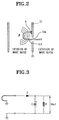
- Figure 1 schematically shows a known microwave oven.
- the conventional microwave oven includes a magnetron MGT for generating microwaves at approximately 2450MHz, a waveguide 10 for transmitting the microwaves generated from the magnetron MGT to food 11 in a cooking chamber 2 and a magnetic field detecting device 100 for detecting the cooking status of the food 11 by sensing microwaves reflected back through the waveguide 10.
- the magnetic field detecting device 100 includes an antenna sensor 101, a diode D and a shield member 120.
- the antenna sensor 101, the diode D and the shield member 120 are fixed to a wall of the waveguide 10 such that the antenna sensor 101 protrudes into the waveguide 10.
- the diode D is connected to one end of the antenna sensor 101 for applying the detected voltage of the standing wave detected by the antenna sensor 101 to a microcomputer 130.
- the microcomputer 130 determines the cooking status of the food 11 from the detected standing wave voltage received through the diode D.
- Figure 2 is a view illustrating the operating principle of a conventional magnetic field detecting device.
- one end of the antenna sensor 101 is grounded on an inner wall of the waveguide 10 by welding, while the other end of the antenna sensor 101 is connected with the diode D through a hole 10a in the waveguide 10.
- the antenna sensor 101 is formed in a semicircular loop having an area A within the waveguide 10.
- a magnetic flux ⁇ which is formed by the standing wave in the waveguide 10, passes through the loop of the antenna sensor 101.
- the microwaves generated by the magnetron MGT propagate along the waveguide 10 to the cooking chamber from where a portion are reflected back along the waeguide 10.
- the combination of the forward and reflected waves produces a standing wave in the wavegurde 10.
- Figure 3 shows the circuit of the magnetic field detecting device shown in Figure 1.
- the anode of the diode D is connected to the antenna sensor 101, and the cathode of the diode D is connected with an electrolytic capacitor C and a resistor R which are connected in parallel to ground.
- the diode D rectifies the voltage signal produced by the loop and the rectified voltage is smoothed by the capacitor C to produce a dc voltage V out across the resistor R.
- a known microwave can adjust various cooking parameters in accordance with the shape or material of the food being cooked.
- the known antenna sensor has a problem as follows. Referring to Figure 2, one end of the antenna sensor 101 is grounded by being soldered inner face of a wall of the waveguide 10. Consequently, the fixing of the antenna sensor 101 is difficult. Furthermore, it is difficult to control the orientation of the antenna sensor 101 resulting in variations in the effective area A of the loop and errors in the output voltage.
- a microwave oven according to the present invention is characterised in that said end of the sensing loop is grounded to the waveguide from the outside.
- the sensor may include a base member received in a hole in the waveguide with the ends of the sensing loop extending through the base member.
- a diode may be included in said loop on the waveguide side of the base member.
- the base member may have a loop supporting member projecting into the waveguide for supporting the loop.
- the base member may have a diode supporting wall structure for supporting the diode.
- the base member may be cup-shaped and house a resistor and a capacitor connected in parallel between the ends of the loop, the base member being open at its waveguide end.
- the loop may be necked and project into the waveguide through a slot.
- the slot may be in a base member received in a hole in the waveguide or in the waveguide itself.
- the loop may be mounted to a printed circuit board and said end of the loop may then be grounded via a screw passing through the printed circuit board and into a wall of the waveguide.
- a first magnetic field detecting device includes an antenna sensor 500 inserted into a waveguide 10, and a shield member 502 on which the antenna sensor 500 is mounted.
- a middle portion of the antenna sensor 500 forms a semicircular loop, which is inserted into the waveguide 10 of a microwave oven through an inserting hole 50a formed on a wall of the waveguide 10.
- the shield member 502 is formed such that the antenna sensor 500 can be inserted into a hole 50a in the waveguide 10 without microwaves leaking from the waveguide 10. Both ends of the loop of the antenna sensor 500 pass through the shield member 502.
- the shield member 502 has a protruding portion 121 for supporting the loop of the antenna sensor 500.
- the area of the loop within the waveguide 10 is preferably in the range 153mm 2 to 314mm 2 .
- a diode D is disposed in one end of the loop to rectify the standing wave voltage induced thereacross.
- the shield member 502 has a flange portion 122 formed thereon to receive the diode D. Accordingly, the diode D is positioned in the waveguide 10 while being supported by the flange portion 122 of the shield member 502.
- the hole 50a in the waveguide 10 corresponds with the protruding portion 121 and the flange portion 122 to air-tightly receive the protruding portion 121 and the flange portion 122 of the shield member 502.
- the shield member 502 is assembled with waveguide 10, simply.
- the protruding portion 121 and the flange portion 122 have a slightly larger radius than the hole 50a and are made of an elastic material.
- the antenna sensor 500 is installed by insering it into the hole 50a and one end of the loop is welded to the outside of the waveguide 10.
- a second magnetic field detecting includes an antenna sensor 600 having a middle portion forming a loop, at one end of which is disposed a diode D, and a shield member 602 on which the antenna sensor 600 is mounted, which is air-tightly inserted into a hole 50a in the waveguide 10.
- the antenna sensor 600 is inserted into the waveguide 10 through the hole 50a.
- the antenna sensor 600 protrudes into the waveguide 10 to detect the standing wave in the waveguide 10.
- the shield member 602 is air-tightly inserted into the hole 50a to support the antenna sensor 600 and prevent leakage of microwaves from the waveguide 10.
- the shield member 602 is in the form of a cup.
- the ends of the antenna sensor 600 pass through the cup.
- the smoothing capacitor C and the parallel resistor R are mounted in the cup.
- the capacitance of the capacitor C is preferably in the range 5 ⁇ F to 50 ⁇ F and the resistor R is preferably in the range 5k ⁇ to 50k ⁇ .
- the cup has at least two locking portions 123 formed at its lip which make the cup easy to insert into the hole 50a but difficult to remove.
- One end of the antenna sensor 600 is grounded by being welded to the outside of the waveguide 10.
- the other end of the antenna sensor 600 is connected to a signal input port of a microcomputer (not shown).
- the capacitor C and the resistor R are contained within a potting compound so that they are not exposed to the inside of the waveguide 10. However, as shown in Figure 5, the diode D is disposed within the waveguide 10. Nevertheless, the diode D may be installed in the cup of the shield member 602 together with the capacitor C and the resistor R.
- a third magnetic field detecting device has the same structure as that of the second preferred embodiment described above with reference to Figure 5, with respect to the feature that the antenna sensor 700 has a loop, and a shield member 702 is air-tightly inserted into a hole 50a in the waveguide 10 while the antenna sensor 700 is positioned and supported by the shield member 702.
- the antenna sensor 700 is inserted into the waveguide 10 through the hole 50a and its middle portion forms a semicircular loop.
- the antenna sensor 700 is exposed standing wave in the waveguide 10 which induces a voltage across the sensor 700.
- the shield member 702 is air-tightly inserted into the hole 50a in the waveguide 10 to prevent leakage of microwaves from the waveguide 10.
- the shield member 702 has a slot 124 on the central portion thereof for supporting the antenna sensor 700.
- the antenna sensor 700 has a neck portion 706 which is held by the slot 124.
- the antenna sensor 700 is made of general-purpose iron wire. It is more preferable, however, that the antenna sensor 700 be made of a high elasticity steel so as to enable the neck portion 706 to be tightly held by the slot 124.
- Two locking portions 704 are formed on the lip of the shield member 702.
- the locking portions 704 are formed such that the sheild member 702 can be easy to install but difficult ro remove.
- the diode D is disposed at one end of the loop portion of the antenna sensor.
- the capacitor and resistor are mounted in the shield member.
- the diode, the capacitor, and the resistor mounted away from the antenna sensor 700, although they could be installed in the shield member 702 as an alternative.
- a magnetic detecting device has a middle portion of an antenna sensor 800 formed into a semicircular loop and the antenna sensor 800 is inserted into the waveguide 10 through a slot 804 in a the wall of the waveguide 10.
- the loop of the antenna sensor 800 is exposed to the standing wave in the waveguide 10 which induces a voltage across it.
- the antenna sensor 800 has a neck portion 802 corresponding to the hole 804.
- the antenna sensor 800 is made of a high elasticity steel, and by its high elasticity, the antenna sensor 800 is tightly held in the slot 804.
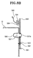
- a fifth magnetic field detecting device includes a printed circuit board 550 having a conductive tracks formed thereon, an antenna sensor 556 fixedly connected on the printed circuit board 550 and a shield member 557 fixing the antenna sensor 556 to the printed circuit board 550.
- a screw coupling hole 552 is formed on a lower portion of the printed circuit board 550 and a ground terminal 553 is formed around the outer circumference of the screw coupling hole 552 and one end of the antenna sensor 556 is connected to the ground terminal 553 by a track on the printed circuit board 550.
- a screw 562 passes through the screw coupling hole 552 and into a hole 552 in the wall of the waveguide 10 and thereby grounds one end of the antenna sensor 556.
- a diode D1 and two resistors R1, R2 are formed on a certain upper portion of the printed circuit board 550.
- the wire connector 564 is connected to a signal input port of a microcomputer (not shown) through the input wire 566, to apply the output voltage of the magnetic field detecting device to the microcomputer.
- a shield member 557 is fixedly connected with the antenna sensor 556.
- the middle portion of the antenna sensor 556 forms a loop and both ends of the loop are passed through the shield member 557 and are soldered on the back face of the printed circuit board 550.
- One soldered end of the antenna sensor 556 is connected with the ground terminal 553 through a track on the printed circuit board 550, while the other soldered end of the antenna sensor 556 is connected to the diode D1 though a track on the printed circuit board 550.
- the shield member 557 has two hook members 557a on the back thereof for engaging the printed circuit board 550.
- the waveguide 10 has a hole 558 formed therein, through which the antenna sensor 556 and the shield member 557 are inserted.
- the waveguide 10 also has a plurality of projections 560 protruding from the outside of the waveguide 10 to position the printed circuit board 550 correctly with respect to the waveguide 10.
- a locking projection 561 protrudes from a lower part of the outside of the waveguide 10 and receive the lower end of the printed circuit board 550 to hold the printed circuit board 550 with respect to the waveguide 10.
- the shield member 557 receiving the antenna sensor 556 and the connector terminal 554 are connected on the printed circuit board 550, while the diode D and the two resistors R1, R2 are connected by tracks on the printed circuit board 550. Also, a screw coupling hole 553 is formed on the lower portion of the printed circuit board 550.
- the waveguide 10 has a plurality of guiding projections 560 protruding therefrom to fit the printed circuit board 550 and a locking projection 561 which is cut away and bent from the wall surface of the waveguide 10.
- the printed circuit board 550 is connected with the waveguide 10, the printed circuit board 550 is guided by the guiding projections 560 and is fitted into the locking projection 561 of the waveguide 10.
- the antenna sensor 556 fixed on the shield member 557 is inserted through the hole 558 in the waveguide 10.
Landscapes
- Physics & Mathematics (AREA)
- Electromagnetism (AREA)
- Engineering & Computer Science (AREA)
- Chemical & Material Sciences (AREA)
- Combustion & Propulsion (AREA)
- Mechanical Engineering (AREA)
- General Engineering & Computer Science (AREA)
- Control Of High-Frequency Heating Circuits (AREA)
- Electric Ovens (AREA)
- Constitution Of High-Frequency Heating (AREA)
- Measuring Magnetic Variables (AREA)
Abstract
Description
Claims (17)
- A microwave oven including a waveguide (10) and a sensor comprising a sensing loop (500; 556; 600; 700; 800) projecting into the waveguide (10), one end of the sensing loop (500; 556; 600; 700; 800) being grounded to the waveguide (10), characterised in that said end of the sensing loop (500; 556; 600; 700; 800) is grounded to the waveguide (10) from the outside.
- A microwave oven according to claim 1, wherein the sensor includes a base member (502; 557; 602) received in a hole in the waveguide (10), the ends of the sensing loop (500; 556; 600) extending through the base member (502; 557; 602).
- A microwave oven according to claim 2, wherein a diode (D) is included in said loop (500; 600) on the waveguide side of the base member (502; 602).
- A microwave oven according to claim 3, wherein the base member (502) has a loop supporting member (121) projecting into the waveguide (10) for supporting the loop (500).
- A microwave oven according to claim 3 or 4, wherein the base member (502) has a diode supporting wall structure (122) for supporting the diode (D).
- A microwave oven according to claim 3, wherein the base member (602) is cup-shaped and houses a resistor (R) and a capacitor (C) connected in parallel between the ends of the loop (600), the base member (602) being open at its waveguide end.
- A microwave oven according to claim 1, wherein the loop (700; 800) is necked and projects into the waveguide through a slot (124; 804).
- A microwave oven according to claim 7, wherein the slot (124) is in a base member (702) received in a hole (50a) in the waveguide (10).
- A microwave oven according to claim 1, wherein the loop (556) is mounted to a printed circuit board (550) and said end of the loop (556) is grounded via a screw passing through the printed circuit board (550) and into a wall of the waveguide (10).
- A microwave oven comprising an antenna sensor including a loop portion which is protruded into a waveguide of the microwave oven, and a wire whose one end is grounded at the waveguide, the wire of the antenna sensor is grounded at an outer side of the waveguide.
- The microwave oven as claimed in claim 10, further comprising a shield member for fixing the antenna sensor in a manner that the loop portion of the antenna sensor is protruded into the waveguide, and for fixing one end of the wire in a manner that the one end of the wire is grounded at the outer side of the waveguide.
- The microwave oven as claimed in claim 11, wherein the shield member includes a projection having a hole thereon for fixing the loop portion of the antenna sensor.
- The microwave oven as claimed in claim 11, wherein the shield member includes a case body in which a magnetic field voltage detecting circuit element is received and is processed by molding.
- The microwave oven as claimed in claim 10, wherein the waveguide includes an inserting hole through which the antenna sensor is received in the waveguide, and the antenna sensor further includes a neck portion which is fixed in the inserting hole of the waveguide.
- The microwave oven as claimed in claim 14, further comprising a shield member having a hole formed thereon for supporting the neck portion of the antenna sensor.
- The microwave oven as claimed in claim 10, further comprising a printed circuit board for fixing the antenna sensor m a manner that the loop portion of the antenna sensor is protruded into the waveguide, and for fixing the wire by grounding the wire.
- The microwave oven as claimed in claim 18, wherein the printed circuit board includes:a screw hole through which a screw is passed through so as to fasten the printed circuit board onto an outer side of the waveguide and to ground the antenna sensor at the waveguide;a coupling hole formed on the outer side of the waveguide through which the screw is fastened;a guiding portion for guiding the printed circuit board while the printed circuit board is fitted into the waveguide; anda locking portion for fixing the printed circuit board which is fitted in the waveguide.
Applications Claiming Priority (4)
| Application Number | Priority Date | Filing Date | Title |
|---|---|---|---|
| KR7600299 | 1999-01-14 | ||
| KR19990000762 | 1999-01-14 | ||
| KR2732999 | 1999-07-07 | ||
| KR19990027329 | 1999-07-07 |
Publications (3)
| Publication Number | Publication Date |
|---|---|
| EP1021069A2 true EP1021069A2 (en) | 2000-07-19 |
| EP1021069A3 EP1021069A3 (en) | 2000-07-26 |
| EP1021069B1 EP1021069B1 (en) | 2007-02-28 |
Family
ID=26634580
Family Applications (1)
| Application Number | Title | Priority Date | Filing Date |
|---|---|---|---|
| EP00300200A Expired - Lifetime EP1021069B1 (en) | 1999-01-14 | 2000-01-12 | Microwave oven with magnetic field sensor |
Country Status (8)
| Country | Link |
|---|---|
| US (1) | US6268597B1 (en) |
| EP (1) | EP1021069B1 (en) |
| JP (1) | JP3299949B2 (en) |
| KR (1) | KR100389005B1 (en) |
| CN (1) | CN1195174C (en) |
| AU (1) | AU728404B2 (en) |
| CA (1) | CA2295394C (en) |
| DE (1) | DE60033584T2 (en) |
Cited By (1)
| Publication number | Priority date | Publication date | Assignee | Title |
|---|---|---|---|---|
| US6452141B1 (en) | 2001-06-30 | 2002-09-17 | Samsung Electronics Co., Ltd. | Microwave oven with magnetic field detecting device |
Families Citing this family (7)
| Publication number | Priority date | Publication date | Assignee | Title |
|---|---|---|---|---|
| GB2335746B (en) * | 1998-03-24 | 2000-10-11 | Samsung Electronics Co Ltd | Microwave oven with food quantity detection |
| US9398646B2 (en) * | 2009-07-10 | 2016-07-19 | Panasonic Intellectual Property Management Co., Ltd. | Microwave heating device and microwave heating control method |
| CN102760931A (en) * | 2011-04-25 | 2012-10-31 | 北京师范大学 | Receiving antenna sensitive to nonuniform action of electromagnetic waves |
| CN102780068A (en) * | 2011-05-09 | 2012-11-14 | 北京师范大学 | Combined antenna for automatic detection technology of direction of arrival of electromagnetic waves |
| CN102780069A (en) * | 2011-05-09 | 2012-11-14 | 北京师范大学 | Receiving antenna with asymmetric response to incidence direction of electromagnetic waves |
| KR101698535B1 (en) | 2014-11-06 | 2017-01-20 | 양기선 | A holder for cable |
| US11047951B2 (en) | 2015-12-17 | 2021-06-29 | Waymo Llc | Surface mount assembled waveguide transition |
Family Cites Families (11)
| Publication number | Priority date | Publication date | Assignee | Title |
|---|---|---|---|---|
| US3412227A (en) * | 1965-11-18 | 1968-11-19 | Tappan Co | Electronic oven protection circuit |
| US3953702A (en) * | 1974-08-13 | 1976-04-27 | Texas Instruments Incorporated | Solid state microwave oven power source |
| US4303818A (en) * | 1979-10-29 | 1981-12-01 | General Electric Company | Microwave oven humidity sensing arrangement |
| FR2520160A1 (en) | 1982-01-20 | 1983-07-22 | Sairem Sarl | Homogeneous thermal treatment of materials by microwaves - transmitted by pairs of aerials penetrating the waveguides |
| GB2117925B (en) * | 1982-02-19 | 1986-02-05 | Hitachi Heating Appl | Heating apparatus of thawing sensor controlled type |
| US4596915A (en) * | 1985-05-07 | 1986-06-24 | Amana Refrigeration, Inc. | Microwave oven having resonant antenna |
| US5254819A (en) * | 1989-12-29 | 1993-10-19 | Matsushita Electric Industrial Co., Ltd. | High-frequency heating apparatus with copper for grounding layer surrounding electromagnetic wave antenna |
| JPH0827316B2 (en) * | 1992-10-23 | 1996-03-21 | 三菱マテリアル株式会社 | Microwave power detector |
| US5378875A (en) * | 1991-12-25 | 1995-01-03 | Mitsubishi Materials Corporation | Microwave oven with power detecting device |
| JPH0827315B2 (en) * | 1992-07-06 | 1996-03-21 | 三菱マテリアル株式会社 | Microwave energy detector |
| US6166364A (en) * | 1999-07-28 | 2000-12-26 | Samsung Electronics Co., Ltd. | Microwave oven having a microwave detecting device |
-
2000
- 2000-01-03 KR KR10-2000-0000019A patent/KR100389005B1/en not_active Expired - Fee Related
- 2000-01-11 US US09/480,692 patent/US6268597B1/en not_active Expired - Lifetime
- 2000-01-12 DE DE60033584T patent/DE60033584T2/en not_active Expired - Lifetime
- 2000-01-12 EP EP00300200A patent/EP1021069B1/en not_active Expired - Lifetime
- 2000-01-12 JP JP2000004012A patent/JP3299949B2/en not_active Expired - Fee Related
- 2000-01-13 CA CA002295394A patent/CA2295394C/en not_active Expired - Fee Related
- 2000-01-13 AU AU10076/00A patent/AU728404B2/en not_active Ceased
- 2000-01-14 CN CNB001002929A patent/CN1195174C/en not_active Expired - Fee Related
Cited By (3)
| Publication number | Priority date | Publication date | Assignee | Title |
|---|---|---|---|---|
| US6452141B1 (en) | 2001-06-30 | 2002-09-17 | Samsung Electronics Co., Ltd. | Microwave oven with magnetic field detecting device |
| GB2377083A (en) * | 2001-06-30 | 2002-12-31 | Samsung Electronics Co Ltd | Waveguide with microwave field detector |
| GB2377083B (en) * | 2001-06-30 | 2003-05-21 | Samsung Electronics Co Ltd | Microwave assembly |
Also Published As
| Publication number | Publication date |
|---|---|
| CA2295394A1 (en) | 2000-07-14 |
| AU1007600A (en) | 2000-08-17 |
| CN1195174C (en) | 2005-03-30 |
| EP1021069A3 (en) | 2000-07-26 |
| CN1261143A (en) | 2000-07-26 |
| US6268597B1 (en) | 2001-07-31 |
| KR100389005B1 (en) | 2003-06-25 |
| DE60033584D1 (en) | 2007-04-12 |
| EP1021069B1 (en) | 2007-02-28 |
| KR20000053370A (en) | 2000-08-25 |
| JP3299949B2 (en) | 2002-07-08 |
| DE60033584T2 (en) | 2007-11-08 |
| AU728404B2 (en) | 2001-01-11 |
| JP2000228282A (en) | 2000-08-15 |
| CA2295394C (en) | 2003-04-08 |
Similar Documents
| Publication | Publication Date | Title |
|---|---|---|
| US4475024A (en) | Wireless food temperature-sensing assembly | |
| EP1021069B1 (en) | Microwave oven with magnetic field sensor | |
| US6452141B1 (en) | Microwave oven with magnetic field detecting device | |
| EP0461269B1 (en) | High-frequency heating device | |
| CA2043436C (en) | High-frequency heating apparatus | |
| US5600531A (en) | Capacitor for magnetron of microwave oven | |
| CN213029670U (en) | Heating device | |
| EP0648066B1 (en) | Noise shielding apparatus for magnetron of microwave oven | |
| JP3051139B2 (en) | High frequency heating equipment | |
| KR100389000B1 (en) | Microwave oven | |
| CN223067224U (en) | Induction cooking device and light shielding structure | |
| JPH018882Y2 (en) | ||
| EP0453928B1 (en) | High frequency heating apparatus | |
| KR100436140B1 (en) | Micro wave oven including magnetic field detector | |
| JP2517201B2 (en) | Cooking device | |
| EP1517343B1 (en) | Capacitor for magnetron of a microwave oven | |
| KR100575659B1 (en) | Microwave Cooking Sensor | |
| KR19990016987A (en) | microwave | |
| JP2000283469A (en) | High frequency heating equipment | |
| JPS6020492A (en) | High frequency heater with wireless temperature probe | |
| JPH03204517A (en) | High-frequency heater | |
| JPS6020491A (en) | High frequency heater with wireless temperature probe |
Legal Events
| Date | Code | Title | Description |
|---|---|---|---|
| PUAI | Public reference made under article 153(3) epc to a published international application that has entered the european phase |
Free format text: ORIGINAL CODE: 0009012 |
|
| PUAL | Search report despatched |
Free format text: ORIGINAL CODE: 0009013 |
|
| AK | Designated contracting states |
Kind code of ref document: A2 Designated state(s): DE FR GB NL |
|
| AX | Request for extension of the european patent |
Free format text: AL;LT;LV;MK;RO;SI |
|
| AK | Designated contracting states |
Kind code of ref document: A3 Designated state(s): AT BE CH CY DE DK ES FI FR GB GR IE IT LI LU MC NL PT SE |
|
| AX | Request for extension of the european patent |
Free format text: AL;LT;LV;MK;RO;SI |
|
| RIN1 | Information on inventor provided before grant (corrected) |
Inventor name: SHON, JONG-CHULL Inventor name: LEE, WON-WOO Inventor name: PARK, TAE-SOO Inventor name: JANG, BO-IN Inventor name: JEONG, JOON-YOUNG Inventor name: LIM, DONG-BIN |
|
| 17P | Request for examination filed |
Effective date: 20010109 |
|
| AKX | Designation fees paid |
Free format text: DE FR GB NL |
|
| RAP1 | Party data changed (applicant data changed or rights of an application transferred) |
Owner name: SAMSUNG ELECTRONICS CO., LTD. |
|
| RIN1 | Information on inventor provided before grant (corrected) |
Inventor name: JEONG, JOON-YOUNG Inventor name: JANG, BO-IN Inventor name: SHON, JONG-CHULL Inventor name: PARK, TAE-SOO Inventor name: LEE, WON-WOO Inventor name: LIM, DONG-BIN |
|
| GRAP | Despatch of communication of intention to grant a patent |
Free format text: ORIGINAL CODE: EPIDOSNIGR1 |
|
| GRAS | Grant fee paid |
Free format text: ORIGINAL CODE: EPIDOSNIGR3 |
|
| GRAA | (expected) grant |
Free format text: ORIGINAL CODE: 0009210 |
|
| AK | Designated contracting states |
Kind code of ref document: B1 Designated state(s): DE FR GB NL |
|
| REG | Reference to a national code |
Ref country code: GB Ref legal event code: FG4D |
|
| REF | Corresponds to: |
Ref document number: 60033584 Country of ref document: DE Date of ref document: 20070412 Kind code of ref document: P |
|
| ET | Fr: translation filed | ||
| PLBE | No opposition filed within time limit |
Free format text: ORIGINAL CODE: 0009261 |
|
| STAA | Information on the status of an ep patent application or granted ep patent |
Free format text: STATUS: NO OPPOSITION FILED WITHIN TIME LIMIT |
|
| 26N | No opposition filed |
Effective date: 20071129 |
|
| PGFP | Annual fee paid to national office [announced via postgrant information from national office to epo] |
Ref country code: GB Payment date: 20110112 Year of fee payment: 12 |
|
| PGFP | Annual fee paid to national office [announced via postgrant information from national office to epo] |
Ref country code: FR Payment date: 20111223 Year of fee payment: 13 Ref country code: NL Payment date: 20111220 Year of fee payment: 13 |
|
| PGFP | Annual fee paid to national office [announced via postgrant information from national office to epo] |
Ref country code: DE Payment date: 20111215 Year of fee payment: 13 |
|
| REG | Reference to a national code |
Ref country code: NL Ref legal event code: V1 Effective date: 20130801 |
|
| GBPC | Gb: european patent ceased through non-payment of renewal fee |
Effective date: 20130112 |
|
| REG | Reference to a national code |
Ref country code: FR Ref legal event code: ST Effective date: 20130930 |
|
| PG25 | Lapsed in a contracting state [announced via postgrant information from national office to epo] |
Ref country code: NL Free format text: LAPSE BECAUSE OF NON-PAYMENT OF DUE FEES Effective date: 20130801 Ref country code: DE Free format text: LAPSE BECAUSE OF NON-PAYMENT OF DUE FEES Effective date: 20130801 |
|
| REG | Reference to a national code |
Ref country code: DE Ref legal event code: R119 Ref document number: 60033584 Country of ref document: DE Effective date: 20130801 |
|
| PG25 | Lapsed in a contracting state [announced via postgrant information from national office to epo] |
Ref country code: FR Free format text: LAPSE BECAUSE OF NON-PAYMENT OF DUE FEES Effective date: 20130131 Ref country code: GB Free format text: LAPSE BECAUSE OF NON-PAYMENT OF DUE FEES Effective date: 20130112 |