EP1016123B1 - Atom probe - Google Patents
Atom probe Download PDFInfo
- Publication number
- EP1016123B1 EP1016123B1 EP98941603A EP98941603A EP1016123B1 EP 1016123 B1 EP1016123 B1 EP 1016123B1 EP 98941603 A EP98941603 A EP 98941603A EP 98941603 A EP98941603 A EP 98941603A EP 1016123 B1 EP1016123 B1 EP 1016123B1
- Authority
- EP
- European Patent Office
- Prior art keywords
- plate
- specimen
- counter electrode
- detector
- atom probe
- Prior art date
- Legal status (The legal status is an assumption and is not a legal conclusion. Google has not performed a legal analysis and makes no representation as to the accuracy of the status listed.)
- Expired - Lifetime
Links
- 239000000523 sample Substances 0.000 title claims description 36
- 150000002500 ions Chemical class 0.000 claims description 52
- 238000000034 method Methods 0.000 claims description 7
- 238000000926 separation method Methods 0.000 claims description 6
- 238000004141 dimensional analysis Methods 0.000 claims description 2
- 239000012212 insulator Substances 0.000 claims description 2
- 239000002184 metal Substances 0.000 claims description 2
- 125000006850 spacer group Chemical group 0.000 claims description 2
- 239000000758 substrate Substances 0.000 claims description 2
- 230000036962 time dependent Effects 0.000 claims description 2
- 238000005259 measurement Methods 0.000 claims 1
- 239000007787 solid Substances 0.000 claims 1
- 230000005684 electric field Effects 0.000 description 14
- 238000001704 evaporation Methods 0.000 description 4
- 230000008020 evaporation Effects 0.000 description 4
- 238000010586 diagram Methods 0.000 description 3
- 238000004458 analytical method Methods 0.000 description 1
- 239000004020 conductor Substances 0.000 description 1
- 229910003460 diamond Inorganic materials 0.000 description 1
- 239000010432 diamond Substances 0.000 description 1
- 238000009413 insulation Methods 0.000 description 1
- 238000012544 monitoring process Methods 0.000 description 1
- 230000003287 optical effect Effects 0.000 description 1
- 238000000992 sputter etching Methods 0.000 description 1
- 238000001269 time-of-flight mass spectrometry Methods 0.000 description 1
Images
Classifications
-
- H—ELECTRICITY
- H01—ELECTRIC ELEMENTS
- H01J—ELECTRIC DISCHARGE TUBES OR DISCHARGE LAMPS
- H01J37/00—Discharge tubes with provision for introducing objects or material to be exposed to the discharge, e.g. for the purpose of examination or processing thereof
- H01J37/26—Electron or ion microscopes; Electron or ion diffraction tubes
- H01J37/285—Emission microscopes, e.g. field-emission microscopes
Definitions
- the present invention relates to an atom probe and in particular to a scanning atom probe.
- a known design of an atom probe is described in an article by A. Cerezo et al published in EMSA Bulletin 20:2 November 1990.
- the design essentially comprises a counter electrode and a detector located some distance (e.g. approx. 600mm) behind the counter electrode. At least a part of the counter electrode is adapted (e.g. by having a hole formed therein) to permit the through-passage of ions.
- a sample to be analysed, in the form of a sharply pointed needle of end radius approximately 20-100nm, is brought in front of the counter electrode so as to be substantially aligned with that part of the counter electrode which is adapted to permit the through-passage of ions.
- the dc voltage V s is less than but near to that required to produce an electric field strength at the needle end which is sufficient to cause ionisation and evaporation of exposed or prominent atoms on the needle end.
- V p When the voltage pulse V p is applied to the sample, the electric field strength is increased, at a well defined point in time for a well defined duration, such that ionisation and evaporation occurs. In this way the point in time at which an ion leaves the sample can be determined.
- the use of a voltage pulse gives rise to the situation that ions are accelerated away from the needle in a time-varying electric field which results in a broad spread in the kinetic energies of the ions travelling to the detector. Thus the kinetic energy of individual ions leaving the sample and travelling to the counter electrode is not well defined.
- the present invention seeks to provide an atom probe which provides a narrow spread of kinetic energies of ions so as to provide improved mass resolution of detected ions.
- the kinetic energy is substantially defined by the voltage potential between specimen and detector.
- an atom probe for analysing the surface of a specimen comprising a detector; a counter electrode which includes a first plate and at least one second plate located between the first plate and the detector; control and power supply means connected to the first and second plates for maintaining at least one second plate at a substantially constant voltage with respect to the detector and for supplying a negative voltage pulse to the first plate wherein the control and supply means is adapted to supply a voltage pulse which has a substantially constant maximum negative voltage for a period of time dependent on the separation of at least one second plate from the specimen, whereby said constant maximum voltage is supplied whilst ions are in transit between the specimen and the at least one second plate.
- the first plate is maintained at substantially the same voltage as the at least one second plate other than when the negative voltage pulse is applied to the first plate when its voltage preferably falls below that of the at least one second plate.
- the at least one second plate and the detector are held at substantially the same voltage so that ions passing the first electrode are decelerated and then coast towards the detector.
- a preferred separation between the first and second plates is less than 250 ⁇ m. This has the advantage of enabling the first plate to be located further than 1 ⁇ m from the tip of the specimen to be analysed (preferably about 5-30 ⁇ m) while still enabling ions leaving the specimen, when accelerated by a potential difference of approximately 10kV, to reach the second plate within about 1 nanosecond. This is approximately the preferred accuracy within which the time of evaporation needs to be known in order to prevent significant loss of resolution.
- the specimen may take the form of a sharply pointed needle of end radius approximately 20-100nm or a substantially flat surface having one or more microtips thereon.
- the final kinetic energy of the ion will not depend strongly on the exact value of the voltage on the first plate at the time of evaporation.
- the spread of kinetic energies of ions accelerated in this way is relatively narrow. Any changes in the voltage of the first plate after an ion has passed the second plate will not affect the kinetic energy of the ion.
- the control and supply means preferably incorporates at least one solid-state switch that provides the voltage pulse to the first plate.
- the use of one or more solid-state switches enables a voltage pulse to be provided which has a relatively smooth rise and fall and a plateau duration of approximately 1ns. Such a voltage pulse is well adapted for use with the atom probe of the present invention.
- the detector is preferably position sensitive such that a three dimensional analysis of the specimen may be undertaken.
- the counter electrode is preferably mounted on drive means to enable the counter electrode to be moved relative to the specimen so as to permit alignment of the counter electrode with a sharply pointed specimen and/or to permit a number of different microtips on a substantially flat surface to be analysed sequentially.
- the atom probe is able to function as a scanning atom probe.
- the specimen may be moved with respect to a fixed/movable counter electrode to afford relative movement.
- At least the first plate of the counter electrode may be generally cone-shaped in the direction away from the detector. This enables the electric field generated at the specimen to be concentrated at only a single microtip, thus preventing interference from any nearby microtips.
- the counter electrode may conveniently be formed from two separately fabricated plates which are then assembled together with insulating spacers which provide insulation between the plates, ensure a suitable separation between the plates and assist in the positioning and relative alignment of the plates.
- the counter electrode may be integrally formed using a combination of metal and insulator layers on a shaped substrate.
- the atom probe essentially consists of a two-part counter electrode 10 and a detector 20 located behind the counter electrode.
- the counter electrode 10 is formed from a first plate 11 and a second plate 12 which are electrically isolated from one another by suitable insulating spacing elements 15 (see Figure 2). At least the first plate 11 is shaped with truncated frusto-conical surfaces at an angle away from the plane of the detector 20, so that the electric field generated between the specimen 30 and the first plate 11 is concentrated at only one microtip 31a, through suitable alignment between the specimen 30 and the counter electrode 10.
- a positive dc voltage V s is applied to the specimen (which is formed from a conductive or semi-conductive material to be analysed) by the control and power supply means (not shown).
- the first plate 11 is held at approximately zero volts until a negative voltage pulse V p is applied.
- V p negative voltage pulse
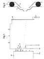
- the negative voltage pulse V p is preferably shaped as shown in Figure 3 with a magnitude of approximately 1-2kV.
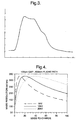
- the dc voltage V s applied to the specimen is preferably about 10kV, although this may be altered considerably (see Figure 4) to match the conditions of the atom probe and the specimen being analysed.
- Factors affecting the dc voltage V s include the dimensions of the microtip, the composition of the specimen, the distance between the specimen and the counter electrode, etc.
- a 1-2% change in field strength changes the ionisation rate by a factor of approximately 10.
- appreciable ionisation is substantially restricted to the top 1-2% of the applied voltage.
- the total applied voltage between the specimen and the first plate is about ten times greater than the voltage pulse, appreciable ionisation can also be said to be primarily restricted to the top 10 - 20% of the voltage pulse. This represents a short period of time during which the ions could have been formed and evaporated, which therefore defines the time of departure of the ions from the microtip reasonably precisely (i.e. to within a few nanoseconds and preferably to within 2 nanoseconds) which is important to ensure high mass resolution of the ions being detected.
- a solid-state switch may be used.
- Such devices are capable of producing high voltage, short duration pulses at a relatively high frequency and the shape of the pulses may be tailored to suit the needs of any particular patent application.
- a voltage pulse produced by such a solid-state switch and suitable for use in the present invention is shown in Figure 3 in which the horizontal divisions each represent 2 nanoseconds, while the vertical scale is arbitrary but linear.
- Such a pulse has a magnitude of about 1-2kV, a relatively smooth rise and fall, within the top 20% (by magnitude) of the voltage pulse, and a plateau extending preferably only for about one or two nanoseconds.
- the use of the voltage pulse such as that shown in Figure 3 in combination with the counter electrode 10, where the first 11 and the second 12 plates are located relatively closely together (e.g. about 100 microns apart) enables the majority of ions (those having a sufficiently low mass/charge ratio given the accelerating voltage) formed on the microtip 31a being analysed, to make the journey between the microtip 31 a and the second plate 12 in a sufficiently short time (e.g. less than one nanosecond) that the voltage on the first plate 11 remains substantially constant, or varies only slowly, whilst the ions are in transit between the microtip 31a and the second plate 12.
- the kinetic energy of ions emerging from the counter electrode 10 primarily depends only on the accelerating voltage between the microtip 31a and the second plate 12 and is substantially independent of the actual voltage between the microtip 31a and the first plate 11 at the time of ionisation. In this way, the long standing problem associated with the spread of energy values of ions produced in a time-varying electric field is substantially overcome.
- the second plate 12 and the detector 20 are preferably grounded, such that ions passing from the counter electrode 10 are first decelerated and then coast towards the detector 20 through a zone which is substantially free of any electric fields.
- a small voltage pulse is produced.
- the time of flight, t f of an ion or ions between leaving the microtip 31a and striking the detector 20 may be accurately established. Since the kinetic energy of such an ion is well known it is possible to calculate the mass-to-charge ratio of the ion and thus to identify what type of ion has been detected.
- the position on the detector 20 where the ions strike corresponds (in a greatly magnified way due to the divergent electric field) to the original position of the atom from which the ion formed on the microtip 31a.
- the detector 20 is able to establish and communicate to the control and power supply means whereabouts each ion strikes the detector 20.
- Suitable detectors 20 for this purpose are known in the art and so their full functioning will not be described here.
- An example of a suitable detector is described in the article by A. Cerezo et al published in EMSA Bulletin 20:2 November, 1990 the contents of which is incorporated herein by reference.
- the counter electrode 10 is preferably mounted on drive means (not shown) such as a piezo-drive to enable the counter electrode 10 to be moved relative to the specimen 30.
- drive means such as a piezo-drive to enable the counter electrode 10 to be moved relative to the specimen 30.
- the counter electrode 10 may be manoeuvred accurately into the correct position in relation to the microtip 31a to be analysed and, where the specimen 30 has a number of microtips 31, 31a formed thereon, the counter electrode 10 may be moved around so as to analyse more than one microtip successively.
- drive means such as a piezo-drive
- a suitable method is to mask the specimen with hard spheres such as diamond spheres and then to etch away the unmasked surface using a technique such as ion milling.
- the atom probe may be operated in a field electron emission mode and a scanned image of the microtips 31, 31a may therefore be produced.
- the counter electrode 10 may then be correctly aligned with each of the microtips to be analysed, before operating the probe as an atom probe, in turn.
- a laser beam shone through the hole in the counter electrode 10 could permit optical alignment.
- Other possible methods of relative positioning are known in the art and could also be used.
Landscapes
- Chemical & Material Sciences (AREA)
- Analytical Chemistry (AREA)
- Other Investigation Or Analysis Of Materials By Electrical Means (AREA)
- Electron Tubes For Measurement (AREA)
Applications Claiming Priority (3)
| Application Number | Priority Date | Filing Date | Title |
|---|---|---|---|
| GBGB9719697.6A GB9719697D0 (en) | 1997-09-16 | 1997-09-16 | Atom probe |
| GB9719697 | 1997-09-16 | ||
| PCT/GB1998/002678 WO1999014793A1 (en) | 1997-09-16 | 1998-09-04 | Atom probe |
Publications (2)
| Publication Number | Publication Date |
|---|---|
| EP1016123A1 EP1016123A1 (en) | 2000-07-05 |
| EP1016123B1 true EP1016123B1 (en) | 2004-03-10 |
Family
ID=10819161
Family Applications (1)
| Application Number | Title | Priority Date | Filing Date |
|---|---|---|---|
| EP98941603A Expired - Lifetime EP1016123B1 (en) | 1997-09-16 | 1998-09-04 | Atom probe |
Country Status (6)
| Country | Link |
|---|---|
| US (1) | US6580069B1 (enExample) |
| EP (1) | EP1016123B1 (enExample) |
| JP (1) | JP2003510757A (enExample) |
| DE (1) | DE69822315T2 (enExample) |
| GB (1) | GB9719697D0 (enExample) |
| WO (1) | WO1999014793A1 (enExample) |
Families Citing this family (14)
| Publication number | Priority date | Publication date | Assignee | Title |
|---|---|---|---|---|
| US6875981B2 (en) * | 2001-03-26 | 2005-04-05 | Kanazawa Institute Of Technology | Scanning atom probe and analysis method utilizing scanning atom probe |
| JP3902925B2 (ja) * | 2001-07-31 | 2007-04-11 | エスアイアイ・ナノテクノロジー株式会社 | 走査型アトムプローブ |
| CA2493212A1 (en) * | 2002-07-24 | 2004-02-26 | Jpk Instruments Ag | Method for locally highly resolved, mass-spectroscopic characterization of surfaces using scanning probe technology |
| US6762415B1 (en) | 2003-04-18 | 2004-07-13 | Imago Scientific Instruments Corporation | Vacuum chamber with recessed viewing tube and imaging device situated therein |
| US7157702B2 (en) * | 2003-06-06 | 2007-01-02 | Imago Scientific Instruments Corporation | High resolution atom probe |
| US6956210B2 (en) | 2003-10-15 | 2005-10-18 | Micron Tchnology, Inc. | Methods for preparing samples for atom probe analysis |
| WO2005104307A2 (en) * | 2004-03-24 | 2005-11-03 | Imago Scientific Instruments Corporation | Laser atom probes |
| CN1977350B (zh) * | 2004-06-03 | 2010-10-06 | 埃美格科学仪器公司 | 激光原子探测方法 |
| WO2006009882A2 (en) * | 2004-06-21 | 2006-01-26 | Imago Scientific Instruments Corporation | Methods and devices for atom probe mass resolution enhancement |
| WO2006101558A2 (en) * | 2004-12-21 | 2006-09-28 | Imago Scientific Instruments Corporation | Laser atom probes |
| GB0512411D0 (en) | 2005-06-17 | 2005-07-27 | Polaron Plc | Atom probe |
| EP1913362A2 (en) * | 2005-07-28 | 2008-04-23 | Imago Scientific Instruments Corporation | Atom probe evaporation processes |
| US20080083882A1 (en) * | 2006-10-06 | 2008-04-10 | Jian Bai | Laser desorption assisted field ionization device and method |
| JP6541798B2 (ja) | 2015-04-21 | 2019-07-10 | カメカ インストゥルメンツ,インコーポレイテッド | 広視野アトムプローブ |
Family Cites Families (10)
| Publication number | Priority date | Publication date | Assignee | Title |
|---|---|---|---|---|
| JPS6079658A (ja) * | 1983-10-07 | 1985-05-07 | Hitachi Ltd | 大気圧イオン化質量分析計 |
| AU6148986A (en) * | 1985-07-23 | 1987-02-10 | Alfred Cerezo | Improvements in atom probes |
| JP3266995B2 (ja) | 1993-07-30 | 2002-03-18 | 株式会社日立製作所 | 導電性部材の観察・計測方法及びその装置 |
| US5440124A (en) * | 1994-07-08 | 1995-08-08 | Wisconsin Alumni Research Foundation | High mass resolution local-electrode atom probe |
| US5614711A (en) * | 1995-05-04 | 1997-03-25 | Indiana University Foundation | Time-of-flight mass spectrometer |
| US5625184A (en) * | 1995-05-19 | 1997-04-29 | Perseptive Biosystems, Inc. | Time-of-flight mass spectrometry analysis of biomolecules |
| DE19547949C2 (de) * | 1995-09-19 | 2000-04-06 | Bruker Daltonik Gmbh | Flugzeitmassenspektrometer |
| US5744797A (en) * | 1995-11-22 | 1998-04-28 | Bruker Analytical Instruments, Inc. | Split-field interface |
| US5864137A (en) * | 1996-10-01 | 1999-01-26 | Genetrace Systems, Inc. | Mass spectrometer |
| JP2939540B2 (ja) * | 1998-01-30 | 1999-08-25 | 科学技術庁金属材料技術研究所長 | パルス励起原子線とパルス紫外光の生成方法およびその装置 |
-
1997
- 1997-09-16 GB GBGB9719697.6A patent/GB9719697D0/en not_active Ceased
-
1998
- 1998-09-04 DE DE69822315T patent/DE69822315T2/de not_active Expired - Lifetime
- 1998-09-04 EP EP98941603A patent/EP1016123B1/en not_active Expired - Lifetime
- 1998-09-04 JP JP2000512237A patent/JP2003510757A/ja active Pending
- 1998-09-04 WO PCT/GB1998/002678 patent/WO1999014793A1/en not_active Ceased
- 1998-09-04 US US09/508,912 patent/US6580069B1/en not_active Expired - Lifetime
Also Published As
| Publication number | Publication date |
|---|---|
| GB9719697D0 (en) | 1997-11-19 |
| DE69822315D1 (de) | 2004-04-15 |
| JP2003510757A (ja) | 2003-03-18 |
| US6580069B1 (en) | 2003-06-17 |
| EP1016123A1 (en) | 2000-07-05 |
| DE69822315T2 (de) | 2004-12-30 |
| WO1999014793A1 (en) | 1999-03-25 |
Similar Documents
| Publication | Publication Date | Title |
|---|---|---|
| EP1016123B1 (en) | Atom probe | |
| US7564026B2 (en) | Linear TOF geometry for high sensitivity at high mass | |
| US5504326A (en) | Spatial-velocity correlation focusing in time-of-flight mass spectrometry | |
| US8829428B2 (en) | Time-of-flight spectrometry and spectroscopy of surfaces | |
| US6674068B1 (en) | Time-of-flight (TOF) mass spectrometer and method of TOF mass spectrometric analysis | |
| US6521887B1 (en) | Time-of-flight ion mass spectrograph | |
| KR102186789B1 (ko) | 2차 이온 질량 분석기 및 2차 이온 질량 분석 방법 | |
| Zhang et al. | Radial velocity distributions of molecular ions produced by matrix-assisted laser desorption/ionization | |
| US7176452B2 (en) | Microfabricated beam modulation device | |
| US3881108A (en) | Ion microprobe analyzer | |
| US4912327A (en) | Pulsed microfocused ion beams | |
| Kurtsiefer et al. | A 2-dimensional detector with high spatial and temporal resolution for metastable rare gas atoms | |
| JP4077881B2 (ja) | 薄被覆層領域における深度プロファイルの確定方法 | |
| JP2641437B2 (ja) | 荷電粒子線装置 | |
| US6469296B1 (en) | Ion acceleration apparatus and method | |
| Gspann | Negatively charged helium-4 clusters | |
| JPH0735801A (ja) | 電磁波検出装置 | |
| JP2590417B2 (ja) | オージェ電子分光装置 | |
| Geno et al. | 252Cf plasma desorption mass spectrometry using a Mamyrin reflectron in a low voltage regime | |
| Kellogg | Ion signal calibration in the imaging atom‐probe with an external, time‐gated image intensifier | |
| Heller et al. | Backscattering spectrometry in the helium ion microscope: Imaging elemental compositions on the nm scale | |
| JPH07294459A (ja) | スパッタ中性粒子質量分析方法 | |
| KR20080100878A (ko) | 초소형 비행 시간 질량 분석기 및 그 제조방법 | |
| KR20020088559A (ko) | 이차이온 질량분석기 | |
| Białas et al. | Miniature ToF mass spectrometer with an integrated glow-discharge ion source |
Legal Events
| Date | Code | Title | Description |
|---|---|---|---|
| PUAI | Public reference made under article 153(3) epc to a published international application that has entered the european phase |
Free format text: ORIGINAL CODE: 0009012 |
|
| 17P | Request for examination filed |
Effective date: 20000320 |
|
| AK | Designated contracting states |
Kind code of ref document: A1 Designated state(s): DE GB |
|
| 17Q | First examination report despatched |
Effective date: 20020814 |
|
| REG | Reference to a national code |
Ref country code: GB Ref legal event code: FG4D |
|
| GRAP | Despatch of communication of intention to grant a patent |
Free format text: ORIGINAL CODE: EPIDOSNIGR1 |
|
| GRAS | Grant fee paid |
Free format text: ORIGINAL CODE: EPIDOSNIGR3 |
|
| GRAA | (expected) grant |
Free format text: ORIGINAL CODE: 0009210 |
|
| AK | Designated contracting states |
Kind code of ref document: B1 Designated state(s): DE GB |
|
| REF | Corresponds to: |
Ref document number: 69822315 Country of ref document: DE Date of ref document: 20040415 Kind code of ref document: P |
|
| PLBE | No opposition filed within time limit |
Free format text: ORIGINAL CODE: 0009261 |
|
| STAA | Information on the status of an ep patent application or granted ep patent |
Free format text: STATUS: NO OPPOSITION FILED WITHIN TIME LIMIT |
|
| 26N | No opposition filed |
Effective date: 20041213 |
|
| PGFP | Annual fee paid to national office [announced via postgrant information from national office to epo] |
Ref country code: DE Payment date: 20100929 Year of fee payment: 13 |
|
| PGFP | Annual fee paid to national office [announced via postgrant information from national office to epo] |
Ref country code: GB Payment date: 20100930 Year of fee payment: 13 |
|
| GBPC | Gb: european patent ceased through non-payment of renewal fee |
Effective date: 20110904 |
|
| REG | Reference to a national code |
Ref country code: DE Ref legal event code: R119 Ref document number: 69822315 Country of ref document: DE Effective date: 20120403 |
|
| PG25 | Lapsed in a contracting state [announced via postgrant information from national office to epo] |
Ref country code: DE Free format text: LAPSE BECAUSE OF NON-PAYMENT OF DUE FEES Effective date: 20120403 |
|
| PG25 | Lapsed in a contracting state [announced via postgrant information from national office to epo] |
Ref country code: GB Free format text: LAPSE BECAUSE OF NON-PAYMENT OF DUE FEES Effective date: 20110904 |