EP1014489A2 - Dielektrische Resonatorantenne - Google Patents
Dielektrische Resonatorantenne Download PDFInfo
- Publication number
- EP1014489A2 EP1014489A2 EP99204261A EP99204261A EP1014489A2 EP 1014489 A2 EP1014489 A2 EP 1014489A2 EP 99204261 A EP99204261 A EP 99204261A EP 99204261 A EP99204261 A EP 99204261A EP 1014489 A2 EP1014489 A2 EP 1014489A2
- Authority
- EP
- European Patent Office
- Prior art keywords
- dielectric resonator
- resonator antenna
- dra
- antenna
- curved surface
- Prior art date
- Legal status (The legal status is an assumption and is not a legal conclusion. Google has not performed a legal analysis and makes no representation as to the accuracy of the status listed.)
- Granted
Links
Images


Classifications
-
- H—ELECTRICITY
- H01—ELECTRIC ELEMENTS
- H01Q—ANTENNAS, i.e. RADIO AERIALS
- H01Q13/00—Waveguide horns or mouths; Slot antennas; Leaky-waveguide antennas; Equivalent structures causing radiation along the transmission path of a guided wave
- H01Q13/20—Non-resonant leaky-waveguide or transmission-line antennas; Equivalent structures causing radiation along the transmission path of a guided wave
- H01Q13/24—Non-resonant leaky-waveguide or transmission-line antennas; Equivalent structures causing radiation along the transmission path of a guided wave constituted by a dielectric or ferromagnetic rod or pipe
-
- H—ELECTRICITY
- H01—ELECTRIC ELEMENTS
- H01Q—ANTENNAS, i.e. RADIO AERIALS
- H01Q1/00—Details of, or arrangements associated with, antennas
- H01Q1/12—Supports; Mounting means
- H01Q1/22—Supports; Mounting means by structural association with other equipment or articles
- H01Q1/24—Supports; Mounting means by structural association with other equipment or articles with receiving set
- H01Q1/241—Supports; Mounting means by structural association with other equipment or articles with receiving set used in mobile communications, e.g. GSM
- H01Q1/242—Supports; Mounting means by structural association with other equipment or articles with receiving set used in mobile communications, e.g. GSM specially adapted for hand-held use
-
- H—ELECTRICITY
- H01—ELECTRIC ELEMENTS
- H01Q—ANTENNAS, i.e. RADIO AERIALS
- H01Q1/00—Details of, or arrangements associated with, antennas
- H01Q1/12—Supports; Mounting means
- H01Q1/22—Supports; Mounting means by structural association with other equipment or articles
- H01Q1/24—Supports; Mounting means by structural association with other equipment or articles with receiving set
-
- H—ELECTRICITY
- H01—ELECTRIC ELEMENTS
- H01Q—ANTENNAS, i.e. RADIO AERIALS
- H01Q9/00—Electrically-short antennas having dimensions not more than twice the operating wavelength and consisting of conductive active radiating elements
- H01Q9/04—Resonant antennas
- H01Q9/0485—Dielectric resonator antennas
Definitions
- the invention relates to a dielectric resonator antenna (DRA).
- DRA dielectric resonator antenna
- the invention further relates to a transmitter, a receiver and a mobile radio device with a dielectric resonator antenna.
- Dielectric resonator antennas are known as miniaturized antennas made of ceramic or another dielectric for microwave frequencies.
- a dielectric resonator the dielectric of which is surrounded by air with a dielectric constant of ⁇ r >> 1, has a discrete spectrum of natural frequencies and natural modes due to the electromagnetic boundary conditions at the interfaces of the dielectric. These are defined by the special solution of the electromagnetic equations for the dielectric under the given boundary conditions at the interfaces.
- the radiation of power is in the foreground with a resonator antenna. Since no conductive structures are used as the radiating element, the skin effect cannot have a negative effect.
- Such antennas therefore have low ohmic losses at high frequencies.
- a compact, miniaturized construction can also be achieved, since the dimensions can be reduced for a preselected natural frequency (transmission and reception frequency) by increasing ⁇ r .
- the dimensions of a DRA given frequency are approximately inversely proportional to ⁇ r .
- An increase in ⁇ r by a factor ⁇ thus results in a reduction in all dimensions by a factor ⁇ and thus the volume by a factor ⁇ 3/2 with a constant resonance frequency.
- a material for a DRA must have good radio frequency capability, low dielectric losses and temperature stability. This severely limits the materials that can be used. Suitable materials have ⁇ r values of typically a maximum of 120.
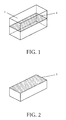
- Such a DR antenna 1 is shown in FIG. 1 in the basic form considered as an example.
- other shapes are also possible, such as cylindrical or spherical geometries.
- Dielectric resonator antennas are resonant components that only work in a narrow band around one of their resonance frequencies (natural frequencies). The problem of antenna miniaturization is equivalent to lowering the operating frequency for given antenna dimensions. Therefore the lowest resonance (TE z 111 mode) is used. This mode has symmetry levels in its electromagnetic fields, one of which is designated symmetry level 2. If the antenna is halved in the plane of symmetry 2 and an electrically conductive surface 3 is attached (for example a metal plate), the resonance frequency remains the same as that of an antenna with the original dimensions.
- a structure is thus obtained in which the same mode is formed at the same frequency. This is shown in Figure 2.
- a further miniaturization can be achieved with this antenna by means of a dielectric with a high dielectric constant ⁇ r .
- a material with low dielectric losses is preferably selected.
- dielectric resonator antenna Such a dielectric resonator antenna is described in the article "Dielectric Resonator Antennas - A review and general design relations for resonant frequency and bandwidth", Rajesh K. Mongia and Prakash Barthia, Intern. Journal of Microwave and Millimeterwave Computer-aided Engineering, Vol. 4 , No. 3, 1994, pages 230-247, which provides an overview of the modes and the radiation characteristics for different shapes, such as cylindrical, spherical and right-angled DRAs. The possible modes and symmetry levels are shown for different shapes (see figure 4, 5, 6 and page 240, left column, lines 1-21) A cuboid dielectric resonator antenna is described in particular in FIG. 9 and the associated description.
- the original structure can be halved without the field distribution or other resonance characteristics for the TE z 111 mode change (page 244, right column, lines 1-7).
- the DRA is excited via a feed line with microwave power by being introduced into the stray field in the vicinity of a microwave line (for example a microstrip line or the end of a coaxial line).
- the object of the invention is therefore to create a dielectric resonator antenna, which offers better options for reducing the dimensions.
- an electrically conductive layer is provided in at least one curved surface in which the tangential component of an electric field of an eigenmode assigned to the dielectric resonator antenna disappears.
- the antenna can be spherical, cuboid or in another geometrical shape, which is chosen, for example, taking into account manufacturing or aesthetic specifications.
- the antenna has a discrete spectrum of propagable eigenmodes and natural frequencies, which are determined by solving the Maxwell equations for electromagnetic fields under the given boundary conditions. Therefore, a given DR antenna is always assigned defined eigenmodes.
- the eigenmodes there are certain distributions of the associated electric field in the antenna, the field vector of which can be divided into a tangential and normal component at each location.
- such curved surfaces are provided with an electrically conductive layer, which are characterized by a vanishing tangential component of the electric field. This means that the same boundary conditions apply to these curved surfaces of the dielectric resonator antenna as to an ideal electrical conductor.
- the conductive layer receives these conditions for the electrical field, and thus also for the associated eigenmode.
- the electrically conductive layer in the curved surface is preferably obtained by cutting the DRA along the curved surface and applying a metallization (e.g. a silver paste) to the cut surface. Therefore, the volume of the DRA can be reduced considerably, although the same mode continues to develop at the same frequency. Since there are several curved surfaces identified in this way, a particularly advantageous surface can be selected, for example, according to the desired degree of miniaturization, the required bandwidth of the antenna that is being produced, and the manufacturing conditions.
- a metallization e.g. a silver paste
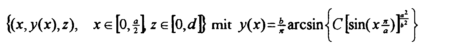
- a cuboid made of a dielectric material with the side lengths a, b and d in the orthogonal directions x, y and z is provided to form the dielectric resonator antenna, and is a curved surface of the shape provided with the electrically conductive layer.
- a rectangular box is one of the basic shapes used for dielectric resonator antennas. This basic form can be described particularly well by means of a Cartesian coordinate system, the zero point of which is advantageously chosen in a corner of the cuboid such that the edges of the cuboid lie on the x, y and z axes and positive side lengths a, b and d arise .
- the curved surfaces can be specified in a particularly simple manner using the above formula.
- a curved Surface such a surface is provided, which is formed by means of a parameter C ⁇ 1.
- a parameter C ⁇ 1 is described because then the task of reducing the dimensions the dielectric resonator antenna is solved particularly well. So that will a significantly greater reduction in the volume of the dielectric resonator antenna achieved than is possible without an electrically conductive layer in a curved surface.
- the object of the invention is achieved by a transmitter, a receiver and solved a mobile radio device with such a dielectric resonator antenna in which an electrically conductive layer in at least one curved surface, in which the tangential component of an electric field associated with one of the dielectric resonator antennas Eigenmode disappears, is provided.
- FIG. 3 shows a dielectric resonator antenna DRA 1 in a basic form with rectangular side faces and side lengths a, b and d in the directions x, y and z of a Cartesian coordinate system.
- the DRA 1 has a discrete spectrum of natural frequencies, which are determined by the geometric shape and the external dimensions as well as by the relative dielectric constant ⁇ r of the material used. In order to use the DRA 1 as an antenna for microwave power at a defined frequency, its natural frequency must be close to the defined frequency.
- the DRA 1 is designed for the center frequency 942.5 MHz of the GSM900 standard as a given frequency.
- the cuboidal DRA 1 thus has dimensions of approximately a ⁇ b ⁇ 30 mm and d ⁇ 5.5 mm. Since this dimension seems too large for an integration in devices of mobile communication, the DRA 1 is reduced, as shown in FIGS. 4A and 4B.
- FIG. 4A shows a cross section through the cuboid DRA 1 in a plane perpendicular to the shortest side length d.
- the side lengths a and b lie in the x and y directions.
- a field distribution of an electric field is drawn in, which belongs to the eigenmode with the lowest frequency of the DRA 1.
- this electrical field distribution has clearly visible two planes of symmetry 4 and 5 which are perpendicular to one another and which are marked in cross-section by broken lines.
- the two planes of symmetry are perpendicular to the plane of the drawing.
- the reduced DRA 8 shown in FIG. 4B is obtained.
- the volume of the DRA 1 can be increased by a factor of 4 to a / 2 * b / while the frequency remains the same.
- the DRA 8 results with the dimensions 15 * 15 * 5.5 mm 3 . However, these dimensions are still so large that there can be an obstacle to their use, particularly in mobile telephones.
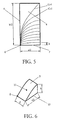
- a zero point 0 of the Cartesian coordinate system is shown in FIG. 5, so that the curved surfaces can be described mathematically.
- a / 2 xb / 2 xd a / 2 and b / 2 are the side lengths in the x and y directions (cf. FIGS. 4B and 5).
- the zero point 0 lies in a corner point of the cuboid DRA 8.
- the curved surfaces of the vanishing tangential component therefore have that Form ⁇ (x, y (x), z), x ⁇ [0, a / 2], z ⁇ [0, d] ⁇ . Since there are several such curved surfaces, an integration parameter C is included, for which 0 ⁇ C ⁇ gilt applies.
- the integration parameter C determines the height h of the remaining DRA.
- the cut one So part is smaller than a / 2 * b / 2, which was achieved by using the planes of symmetry Size.
- This method is in principle for every value of C and thus for any small one h possible so that there is no fundamental limit to the reduction in dimensions a DRA 1 with a constant resonance frequency.
- other parameters can how the bandwidth limit the practically applicable degree of miniaturization.
- the resulting DRA 9 is shown in FIG. 6.
- the plane of symmetry 10 as can already be seen in FIG. 4B, is also a metallized one curved surface 11. Since the height h can be much smaller than b / 2, the resonance frequency however, the same as a rectangular DRA 8 with flat surfaces of dimensions d x a / 2 x b / 2, it becomes a miniaturized DRA 9 with the same Created resonance frequency.
- FIG. 7 shows in a block diagram the function blocks of a transmit and one Reception path of a mobile radio device with a DRA 9, such as one Mobile phone conforms to the GSM standard.
- the DRA 9 is equipped with an antenna switch or frequency duplexer 12 coupled in a receive or transmit mode connects the receive or transmit path to the DRA 9.
- reception mode the analog radio signals arrive at an A / D converter via a receiving circuit 13 14.
- the digital signals generated are demodulated in a demodulator 15 and then fed to a digital signal processor (DSP) 16.
- DSP 16 digital signal processor
- the DSP 16 successively the functions equalization, decryption, not shown in detail Channel decoding and speech decoding performed.
- analog signals are generated which are output via a loudspeaker 18.
- the analog voice signals recorded by a microphone 19 converted with an A / D converter 20 and then fed to a DSP 21.
- the DSP 21 performs the speech coding functions which are complementary to the receiving operation, Channel coding and encryption through, all functions of one single DSP.
- the binary coded data words are in one Modulator 22 GMSK modulated and then in a D / A converter 23 into analog radio signals converted.
- a transmitter output stage 24 with a power amplifier produces this Radio signal to be transmitted via the DRA 9.
- the description of the transmission or reception path 9, 13, 14, 15, 16, 17, 18 or 9, 19, 20, 21, 22, 23, 24 corresponds to that of a single transmitter or receiver.
- the frequency duplexer 12 does not have to be provided, but use the send and receive path its own DRA 9 as an antenna.
- Can be used in any other area of radio transmission e.g. for cordless phones according to DECT or CT, for directional or trunked radio devices or pagers).
- the DRA 9 can be adapted to the transmission frequency.
Landscapes
- Engineering & Computer Science (AREA)
- Computer Networks & Wireless Communication (AREA)
- Details Of Aerials (AREA)
- Aerials With Secondary Devices (AREA)
- Waveguide Aerials (AREA)
- Control Of Motors That Do Not Use Commutators (AREA)
Abstract
Description
- Figur 1:
- eine dielektrische Resonatorantenne,
- Figur 2:
- eine halbierte dielektrische Resonatorantenne mit einer elektrisch leitenden Schicht in einer Symmetrieebene,
- Figur 3:
- eine quaderförmige Grundform der dielektrischen Resonatorantenne mit Seitenlängen a, b und d,
- Figur 4A:
- eine Feldverteilung eines elektrischen Feldes einer Eigenmode einer quaderförmigen dielektrischen Resonatorantenne in einer Ebene senkrecht zur kürzesten Seitenlänge,
- Figur 4B:
- eine entlang der Symmetrieebenen der dielektrischen Resonatorantenne verkleinerte Antenne mit der Feldverteilung,
- Figur 5:
- einen Querschnitt durch die verkleinerte dielektrische Resonatorantenne mit gekrümmten Flächen, in denen die Tangentialkomponente des elektrischen Feldes verschwindet,
- Figur 6:
- eine verkleinerte dielektrische Resonatorantenne mit einer Reduzierung des Volumens entlang einer gekrümmten Fläche und
- Figur 7:
- ein vereinfachtes Blockschaltbild eines Mobilfunkgerätes mit Sende- und Empfangspfad und einer dielektrischen Resonatorantenne.
Claims (6)
- Dielektrische Resonatorantenne (9),
dadurch gekennzeichnet,
daß eine elektrisch leitende Schicht in wenigstens einer gekrümmten Fläche (11), in der die Tangentialkomponente eines elektrischen Feldes einer der dielektrischen Resonatorantenne (9) zugeordneten Eigenmode verschwindet, vorgesehen ist. - Dielektrische Resonatorantenne (9) nach Anspruch 1,
dadurch gekennzeichnet,
daß zur Bildung der dielektrischen Resonatorantenne (9) ein Quader aus einem dielektrischen Material mit den Seitenlängen a, b und d in den orthogonalen Richtungen x, y und z vorgesehen ist,
und daß eine gekrümmte Fläche (11) der Formmit der elektrisch leitfähigen Schicht versehen ist.
- Dielektrische Resonatorantenne (9) nach Anspruch 2,
dadurch gekennzeichnet,
daß zur Bildung der gekrümmten Fläche (11) eine solche Fläche vorgesehen ist, die mittels eines Parameters C<1 gebildet ist. - Mobilfunkgerät (9, 13, 14, 15, 16, 17, 18, 19, 20, 21, 22, 23, 24) mit einer dielektrischen Resonatorantenne (9),
dadurch gekennzeichnet,
daß in der dielektrischen Resonatorantenne (9) eine elektrisch leitende Schicht in wenigstens einer gekrümmten Fläche (11), in der die Tangentialkomponente eines elektrischen Feldes einer der dielektrischen Resonatorantenne (9) zugeordneten Eigenmode verschwindet, vorgesehen ist. - Empfänger (9, 19, 20, 21, 22, 23, 24) mit einer dielektrischen Resonatorantenne (9),
dadurch gekennzeichnet,
daß in der dielektrischen Resonatorantenne (9) eine elektrisch leitende Schicht in wenigstens einer gekrümmten Fläche (11), in der die Tangentialkomponente eines elektrischen Feldes einer der dielektrischen Resonatorantenne (9) zugeordneten Eigenmode verschwindet, vorgesehen ist. - Sender (9, 13, 14, 15, 16, 17, 18) mit einer dielektrischen Resonatorantenne (9),
dadurch gekennzeichnet,
daß in der dielektrischen Resonatorantenne (9) eine elektrisch leitende Schicht in wenigstens einer gekrümmten Fläche (11), in der die Tangentialkomponente eines elektrischen Feldes einer der dielektrischen Resonatorantenne (9) zugeordneten Eigenmode verschwindet, vorgesehen ist.
Applications Claiming Priority (2)
| Application Number | Priority Date | Filing Date | Title |
|---|---|---|---|
| DE19858799 | 1998-12-18 | ||
| DE19858799A DE19858799A1 (de) | 1998-12-18 | 1998-12-18 | Dielektrische Resonatorantenne |
Publications (3)
| Publication Number | Publication Date |
|---|---|
| EP1014489A2 true EP1014489A2 (de) | 2000-06-28 |
| EP1014489A3 EP1014489A3 (de) | 2002-01-16 |
| EP1014489B1 EP1014489B1 (de) | 2003-11-12 |
Family
ID=7891791
Family Applications (1)
| Application Number | Title | Priority Date | Filing Date |
|---|---|---|---|
| EP99204261A Expired - Lifetime EP1014489B1 (de) | 1998-12-18 | 1999-12-09 | Dielektrische Resonatorantenne |
Country Status (7)
| Country | Link |
|---|---|
| US (1) | US6373441B1 (de) |
| EP (1) | EP1014489B1 (de) |
| JP (1) | JP2000209019A (de) |
| KR (1) | KR100710729B1 (de) |
| CN (1) | CN1126194C (de) |
| DE (2) | DE19858799A1 (de) |
| TW (1) | TW456070B (de) |
Families Citing this family (147)
| Publication number | Priority date | Publication date | Assignee | Title |
|---|---|---|---|---|
| GB2387995B (en) * | 2002-04-23 | 2006-01-25 | Hutchison Whampoa Three G Ip | Improved portable telecommunication terminal |
| GB0219011D0 (en) * | 2002-08-15 | 2002-09-25 | Antenova Ltd | Improvements relating to antenna isolation and diversity in relation to dielectric resonator antennas |
| JP4217709B2 (ja) | 2003-02-18 | 2009-02-04 | 財団法人国際科学振興財団 | 携帯端末用アンテナおよびそれを用いた携帯端末 |
| US7710325B2 (en) * | 2006-08-15 | 2010-05-04 | Intel Corporation | Multi-band dielectric resonator antenna |
| EP2165416A1 (de) * | 2007-06-01 | 2010-03-24 | Nxp B.V. | Mems-resonatoren |
| US8253643B2 (en) | 2007-06-07 | 2012-08-28 | Hitachi Metals Ltd. | Chip antenna and its production method, and antenna apparatus and communications apparatus comprising such chip antenna |
| US9123995B2 (en) | 2012-03-06 | 2015-09-01 | City University Of Hong Kong | Dielectric antenna and method of discretely emitting radiation pattern using same |
| US9525524B2 (en) | 2013-05-31 | 2016-12-20 | At&T Intellectual Property I, L.P. | Remote distributed antenna system |
| US9999038B2 (en) | 2013-05-31 | 2018-06-12 | At&T Intellectual Property I, L.P. | Remote distributed antenna system |
| US8897697B1 (en) | 2013-11-06 | 2014-11-25 | At&T Intellectual Property I, Lp | Millimeter-wave surface-wave communications |
| US9768833B2 (en) | 2014-09-15 | 2017-09-19 | At&T Intellectual Property I, L.P. | Method and apparatus for sensing a condition in a transmission medium of electromagnetic waves |
| US10063280B2 (en) | 2014-09-17 | 2018-08-28 | At&T Intellectual Property I, L.P. | Monitoring and mitigating conditions in a communication network |
| US9615269B2 (en) | 2014-10-02 | 2017-04-04 | At&T Intellectual Property I, L.P. | Method and apparatus that provides fault tolerance in a communication network |
| US9685992B2 (en) | 2014-10-03 | 2017-06-20 | At&T Intellectual Property I, L.P. | Circuit panel network and methods thereof |
| US9503189B2 (en) | 2014-10-10 | 2016-11-22 | At&T Intellectual Property I, L.P. | Method and apparatus for arranging communication sessions in a communication system |
| US9973299B2 (en) | 2014-10-14 | 2018-05-15 | At&T Intellectual Property I, L.P. | Method and apparatus for adjusting a mode of communication in a communication network |
| US9577306B2 (en) | 2014-10-21 | 2017-02-21 | At&T Intellectual Property I, L.P. | Guided-wave transmission device and methods for use therewith |
| US9653770B2 (en) | 2014-10-21 | 2017-05-16 | At&T Intellectual Property I, L.P. | Guided wave coupler, coupling module and methods for use therewith |
| US9312919B1 (en) | 2014-10-21 | 2016-04-12 | At&T Intellectual Property I, Lp | Transmission device with impairment compensation and methods for use therewith |
| US9627768B2 (en) | 2014-10-21 | 2017-04-18 | At&T Intellectual Property I, L.P. | Guided-wave transmission device with non-fundamental mode propagation and methods for use therewith |
| US9769020B2 (en) | 2014-10-21 | 2017-09-19 | At&T Intellectual Property I, L.P. | Method and apparatus for responding to events affecting communications in a communication network |
| US9780834B2 (en) | 2014-10-21 | 2017-10-03 | At&T Intellectual Property I, L.P. | Method and apparatus for transmitting electromagnetic waves |
| US9800327B2 (en) | 2014-11-20 | 2017-10-24 | At&T Intellectual Property I, L.P. | Apparatus for controlling operations of a communication device and methods thereof |
| US9544006B2 (en) | 2014-11-20 | 2017-01-10 | At&T Intellectual Property I, L.P. | Transmission device with mode division multiplexing and methods for use therewith |
| US10340573B2 (en) | 2016-10-26 | 2019-07-02 | At&T Intellectual Property I, L.P. | Launcher with cylindrical coupling device and methods for use therewith |
| US10243784B2 (en) | 2014-11-20 | 2019-03-26 | At&T Intellectual Property I, L.P. | System for generating topology information and methods thereof |
| US9461706B1 (en) | 2015-07-31 | 2016-10-04 | At&T Intellectual Property I, Lp | Method and apparatus for exchanging communication signals |
| US9997819B2 (en) | 2015-06-09 | 2018-06-12 | At&T Intellectual Property I, L.P. | Transmission medium and method for facilitating propagation of electromagnetic waves via a core |
| US9954287B2 (en) | 2014-11-20 | 2018-04-24 | At&T Intellectual Property I, L.P. | Apparatus for converting wireless signals and electromagnetic waves and methods thereof |
| US9742462B2 (en) | 2014-12-04 | 2017-08-22 | At&T Intellectual Property I, L.P. | Transmission medium and communication interfaces and methods for use therewith |
| US10009067B2 (en) | 2014-12-04 | 2018-06-26 | At&T Intellectual Property I, L.P. | Method and apparatus for configuring a communication interface |
| US9876570B2 (en) | 2015-02-20 | 2018-01-23 | At&T Intellectual Property I, Lp | Guided-wave transmission device with non-fundamental mode propagation and methods for use therewith |
| US9749013B2 (en) | 2015-03-17 | 2017-08-29 | At&T Intellectual Property I, L.P. | Method and apparatus for reducing attenuation of electromagnetic waves guided by a transmission medium |
| US10224981B2 (en) | 2015-04-24 | 2019-03-05 | At&T Intellectual Property I, Lp | Passive electrical coupling device and methods for use therewith |
| US9705561B2 (en) | 2015-04-24 | 2017-07-11 | At&T Intellectual Property I, L.P. | Directional coupling device and methods for use therewith |
| US9793954B2 (en) | 2015-04-28 | 2017-10-17 | At&T Intellectual Property I, L.P. | Magnetic coupling device and methods for use therewith |
| US9871282B2 (en) | 2015-05-14 | 2018-01-16 | At&T Intellectual Property I, L.P. | At least one transmission medium having a dielectric surface that is covered at least in part by a second dielectric |
| US9490869B1 (en) | 2015-05-14 | 2016-11-08 | At&T Intellectual Property I, L.P. | Transmission medium having multiple cores and methods for use therewith |
| US9748626B2 (en) | 2015-05-14 | 2017-08-29 | At&T Intellectual Property I, L.P. | Plurality of cables having different cross-sectional shapes which are bundled together to form a transmission medium |
| US10650940B2 (en) | 2015-05-15 | 2020-05-12 | At&T Intellectual Property I, L.P. | Transmission medium having a conductive material and methods for use therewith |
| US9917341B2 (en) | 2015-05-27 | 2018-03-13 | At&T Intellectual Property I, L.P. | Apparatus and method for launching electromagnetic waves and for modifying radial dimensions of the propagating electromagnetic waves |
| US9866309B2 (en) | 2015-06-03 | 2018-01-09 | At&T Intellectual Property I, Lp | Host node device and methods for use therewith |
| US9912381B2 (en) | 2015-06-03 | 2018-03-06 | At&T Intellectual Property I, Lp | Network termination and methods for use therewith |
| US10812174B2 (en) | 2015-06-03 | 2020-10-20 | At&T Intellectual Property I, L.P. | Client node device and methods for use therewith |
| US9913139B2 (en) | 2015-06-09 | 2018-03-06 | At&T Intellectual Property I, L.P. | Signal fingerprinting for authentication of communicating devices |
| US9820146B2 (en) | 2015-06-12 | 2017-11-14 | At&T Intellectual Property I, L.P. | Method and apparatus for authentication and identity management of communicating devices |
| US9667317B2 (en) | 2015-06-15 | 2017-05-30 | At&T Intellectual Property I, L.P. | Method and apparatus for providing security using network traffic adjustments |
| US9865911B2 (en) | 2015-06-25 | 2018-01-09 | At&T Intellectual Property I, L.P. | Waveguide system for slot radiating first electromagnetic waves that are combined into a non-fundamental wave mode second electromagnetic wave on a transmission medium |
| US9509415B1 (en) | 2015-06-25 | 2016-11-29 | At&T Intellectual Property I, L.P. | Methods and apparatus for inducing a fundamental wave mode on a transmission medium |
| US9640850B2 (en) | 2015-06-25 | 2017-05-02 | At&T Intellectual Property I, L.P. | Methods and apparatus for inducing a non-fundamental wave mode on a transmission medium |
| US10044409B2 (en) | 2015-07-14 | 2018-08-07 | At&T Intellectual Property I, L.P. | Transmission medium and methods for use therewith |
| US10205655B2 (en) | 2015-07-14 | 2019-02-12 | At&T Intellectual Property I, L.P. | Apparatus and methods for communicating utilizing an antenna array and multiple communication paths |
| US9722318B2 (en) | 2015-07-14 | 2017-08-01 | At&T Intellectual Property I, L.P. | Method and apparatus for coupling an antenna to a device |
| US9882257B2 (en) | 2015-07-14 | 2018-01-30 | At&T Intellectual Property I, L.P. | Method and apparatus for launching a wave mode that mitigates interference |
| US9628116B2 (en) | 2015-07-14 | 2017-04-18 | At&T Intellectual Property I, L.P. | Apparatus and methods for transmitting wireless signals |
| US9853342B2 (en) | 2015-07-14 | 2017-12-26 | At&T Intellectual Property I, L.P. | Dielectric transmission medium connector and methods for use therewith |
| US9847566B2 (en) | 2015-07-14 | 2017-12-19 | At&T Intellectual Property I, L.P. | Method and apparatus for adjusting a field of a signal to mitigate interference |
| US10148016B2 (en) | 2015-07-14 | 2018-12-04 | At&T Intellectual Property I, L.P. | Apparatus and methods for communicating utilizing an antenna array |
| US10320586B2 (en) | 2015-07-14 | 2019-06-11 | At&T Intellectual Property I, L.P. | Apparatus and methods for generating non-interfering electromagnetic waves on an insulated transmission medium |
| US9793951B2 (en) | 2015-07-15 | 2017-10-17 | At&T Intellectual Property I, L.P. | Method and apparatus for launching a wave mode that mitigates interference |
| US10090606B2 (en) | 2015-07-15 | 2018-10-02 | At&T Intellectual Property I, L.P. | Antenna system with dielectric array and methods for use therewith |
| US9948333B2 (en) | 2015-07-23 | 2018-04-17 | At&T Intellectual Property I, L.P. | Method and apparatus for wireless communications to mitigate interference |
| US9912027B2 (en) | 2015-07-23 | 2018-03-06 | At&T Intellectual Property I, L.P. | Method and apparatus for exchanging communication signals |
| US9749053B2 (en) | 2015-07-23 | 2017-08-29 | At&T Intellectual Property I, L.P. | Node device, repeater and methods for use therewith |
| US9871283B2 (en) | 2015-07-23 | 2018-01-16 | At&T Intellectual Property I, Lp | Transmission medium having a dielectric core comprised of plural members connected by a ball and socket configuration |
| US9967173B2 (en) | 2015-07-31 | 2018-05-08 | At&T Intellectual Property I, L.P. | Method and apparatus for authentication and identity management of communicating devices |
| US9735833B2 (en) | 2015-07-31 | 2017-08-15 | At&T Intellectual Property I, L.P. | Method and apparatus for communications management in a neighborhood network |
| US9904535B2 (en) | 2015-09-14 | 2018-02-27 | At&T Intellectual Property I, L.P. | Method and apparatus for distributing software |
| US9769128B2 (en) | 2015-09-28 | 2017-09-19 | At&T Intellectual Property I, L.P. | Method and apparatus for encryption of communications over a network |
| US9729197B2 (en) | 2015-10-01 | 2017-08-08 | At&T Intellectual Property I, L.P. | Method and apparatus for communicating network management traffic over a network |
| US9876264B2 (en) | 2015-10-02 | 2018-01-23 | At&T Intellectual Property I, Lp | Communication system, guided wave switch and methods for use therewith |
| US10355367B2 (en) | 2015-10-16 | 2019-07-16 | At&T Intellectual Property I, L.P. | Antenna structure for exchanging wireless signals |
| US10374315B2 (en) | 2015-10-28 | 2019-08-06 | Rogers Corporation | Broadband multiple layer dielectric resonator antenna and method of making the same |
| US11367959B2 (en) | 2015-10-28 | 2022-06-21 | Rogers Corporation | Broadband multiple layer dielectric resonator antenna and method of making the same |
| US10355361B2 (en) | 2015-10-28 | 2019-07-16 | Rogers Corporation | Dielectric resonator antenna and method of making the same |
| US10601137B2 (en) | 2015-10-28 | 2020-03-24 | Rogers Corporation | Broadband multiple layer dielectric resonator antenna and method of making the same |
| US10476164B2 (en) | 2015-10-28 | 2019-11-12 | Rogers Corporation | Broadband multiple layer dielectric resonator antenna and method of making the same |
| US9860075B1 (en) | 2016-08-26 | 2018-01-02 | At&T Intellectual Property I, L.P. | Method and communication node for broadband distribution |
| US10135146B2 (en) | 2016-10-18 | 2018-11-20 | At&T Intellectual Property I, L.P. | Apparatus and methods for launching guided waves via circuits |
| US10135147B2 (en) | 2016-10-18 | 2018-11-20 | At&T Intellectual Property I, L.P. | Apparatus and methods for launching guided waves via an antenna |
| US10340600B2 (en) | 2016-10-18 | 2019-07-02 | At&T Intellectual Property I, L.P. | Apparatus and methods for launching guided waves via plural waveguide systems |
| US10374316B2 (en) | 2016-10-21 | 2019-08-06 | At&T Intellectual Property I, L.P. | System and dielectric antenna with non-uniform dielectric |
| US10811767B2 (en) | 2016-10-21 | 2020-10-20 | At&T Intellectual Property I, L.P. | System and dielectric antenna with convex dielectric radome |
| US9991580B2 (en) | 2016-10-21 | 2018-06-05 | At&T Intellectual Property I, L.P. | Launcher and coupling system for guided wave mode cancellation |
| US9876605B1 (en) | 2016-10-21 | 2018-01-23 | At&T Intellectual Property I, L.P. | Launcher and coupling system to support desired guided wave mode |
| US10312567B2 (en) | 2016-10-26 | 2019-06-04 | At&T Intellectual Property I, L.P. | Launcher with planar strip antenna and methods for use therewith |
| US10225025B2 (en) | 2016-11-03 | 2019-03-05 | At&T Intellectual Property I, L.P. | Method and apparatus for detecting a fault in a communication system |
| US10291334B2 (en) | 2016-11-03 | 2019-05-14 | At&T Intellectual Property I, L.P. | System for detecting a fault in a communication system |
| US10224634B2 (en) | 2016-11-03 | 2019-03-05 | At&T Intellectual Property I, L.P. | Methods and apparatus for adjusting an operational characteristic of an antenna |
| US10498044B2 (en) | 2016-11-03 | 2019-12-03 | At&T Intellectual Property I, L.P. | Apparatus for configuring a surface of an antenna |
| US10340601B2 (en) | 2016-11-23 | 2019-07-02 | At&T Intellectual Property I, L.P. | Multi-antenna system and methods for use therewith |
| US10090594B2 (en) | 2016-11-23 | 2018-10-02 | At&T Intellectual Property I, L.P. | Antenna system having structural configurations for assembly |
| US10535928B2 (en) | 2016-11-23 | 2020-01-14 | At&T Intellectual Property I, L.P. | Antenna system and methods for use therewith |
| US10340603B2 (en) | 2016-11-23 | 2019-07-02 | At&T Intellectual Property I, L.P. | Antenna system having shielded structural configurations for assembly |
| US10178445B2 (en) | 2016-11-23 | 2019-01-08 | At&T Intellectual Property I, L.P. | Methods, devices, and systems for load balancing between a plurality of waveguides |
| US10361489B2 (en) | 2016-12-01 | 2019-07-23 | At&T Intellectual Property I, L.P. | Dielectric dish antenna system and methods for use therewith |
| US10305190B2 (en) | 2016-12-01 | 2019-05-28 | At&T Intellectual Property I, L.P. | Reflecting dielectric antenna system and methods for use therewith |
| US10637149B2 (en) | 2016-12-06 | 2020-04-28 | At&T Intellectual Property I, L.P. | Injection molded dielectric antenna and methods for use therewith |
| US9927517B1 (en) | 2016-12-06 | 2018-03-27 | At&T Intellectual Property I, L.P. | Apparatus and methods for sensing rainfall |
| US10694379B2 (en) | 2016-12-06 | 2020-06-23 | At&T Intellectual Property I, L.P. | Waveguide system with device-based authentication and methods for use therewith |
| US10439675B2 (en) | 2016-12-06 | 2019-10-08 | At&T Intellectual Property I, L.P. | Method and apparatus for repeating guided wave communication signals |
| US10326494B2 (en) | 2016-12-06 | 2019-06-18 | At&T Intellectual Property I, L.P. | Apparatus for measurement de-embedding and methods for use therewith |
| US10382976B2 (en) | 2016-12-06 | 2019-08-13 | At&T Intellectual Property I, L.P. | Method and apparatus for managing wireless communications based on communication paths and network device positions |
| US10819035B2 (en) | 2016-12-06 | 2020-10-27 | At&T Intellectual Property I, L.P. | Launcher with helical antenna and methods for use therewith |
| US10755542B2 (en) | 2016-12-06 | 2020-08-25 | At&T Intellectual Property I, L.P. | Method and apparatus for surveillance via guided wave communication |
| US10135145B2 (en) | 2016-12-06 | 2018-11-20 | At&T Intellectual Property I, L.P. | Apparatus and methods for generating an electromagnetic wave along a transmission medium |
| US10020844B2 (en) | 2016-12-06 | 2018-07-10 | T&T Intellectual Property I, L.P. | Method and apparatus for broadcast communication via guided waves |
| US10727599B2 (en) | 2016-12-06 | 2020-07-28 | At&T Intellectual Property I, L.P. | Launcher with slot antenna and methods for use therewith |
| US10389029B2 (en) | 2016-12-07 | 2019-08-20 | At&T Intellectual Property I, L.P. | Multi-feed dielectric antenna system with core selection and methods for use therewith |
| US10139820B2 (en) | 2016-12-07 | 2018-11-27 | At&T Intellectual Property I, L.P. | Method and apparatus for deploying equipment of a communication system |
| US10446936B2 (en) | 2016-12-07 | 2019-10-15 | At&T Intellectual Property I, L.P. | Multi-feed dielectric antenna system and methods for use therewith |
| US10027397B2 (en) | 2016-12-07 | 2018-07-17 | At&T Intellectual Property I, L.P. | Distributed antenna system and methods for use therewith |
| US10547348B2 (en) | 2016-12-07 | 2020-01-28 | At&T Intellectual Property I, L.P. | Method and apparatus for switching transmission mediums in a communication system |
| US10359749B2 (en) | 2016-12-07 | 2019-07-23 | At&T Intellectual Property I, L.P. | Method and apparatus for utilities management via guided wave communication |
| US10243270B2 (en) | 2016-12-07 | 2019-03-26 | At&T Intellectual Property I, L.P. | Beam adaptive multi-feed dielectric antenna system and methods for use therewith |
| US10168695B2 (en) | 2016-12-07 | 2019-01-01 | At&T Intellectual Property I, L.P. | Method and apparatus for controlling an unmanned aircraft |
| US9893795B1 (en) | 2016-12-07 | 2018-02-13 | At&T Intellectual Property I, Lp | Method and repeater for broadband distribution |
| US10916969B2 (en) | 2016-12-08 | 2021-02-09 | At&T Intellectual Property I, L.P. | Method and apparatus for providing power using an inductive coupling |
| US10389037B2 (en) | 2016-12-08 | 2019-08-20 | At&T Intellectual Property I, L.P. | Apparatus and methods for selecting sections of an antenna array and use therewith |
| US9998870B1 (en) | 2016-12-08 | 2018-06-12 | At&T Intellectual Property I, L.P. | Method and apparatus for proximity sensing |
| US10938108B2 (en) | 2016-12-08 | 2021-03-02 | At&T Intellectual Property I, L.P. | Frequency selective multi-feed dielectric antenna system and methods for use therewith |
| US10530505B2 (en) | 2016-12-08 | 2020-01-07 | At&T Intellectual Property I, L.P. | Apparatus and methods for launching electromagnetic waves along a transmission medium |
| US10103422B2 (en) | 2016-12-08 | 2018-10-16 | At&T Intellectual Property I, L.P. | Method and apparatus for mounting network devices |
| US9911020B1 (en) | 2016-12-08 | 2018-03-06 | At&T Intellectual Property I, L.P. | Method and apparatus for tracking via a radio frequency identification device |
| US10069535B2 (en) | 2016-12-08 | 2018-09-04 | At&T Intellectual Property I, L.P. | Apparatus and methods for launching electromagnetic waves having a certain electric field structure |
| US10326689B2 (en) | 2016-12-08 | 2019-06-18 | At&T Intellectual Property I, L.P. | Method and system for providing alternative communication paths |
| US10411356B2 (en) | 2016-12-08 | 2019-09-10 | At&T Intellectual Property I, L.P. | Apparatus and methods for selectively targeting communication devices with an antenna array |
| US10601494B2 (en) | 2016-12-08 | 2020-03-24 | At&T Intellectual Property I, L.P. | Dual-band communication device and method for use therewith |
| US10777873B2 (en) | 2016-12-08 | 2020-09-15 | At&T Intellectual Property I, L.P. | Method and apparatus for mounting network devices |
| US9838896B1 (en) | 2016-12-09 | 2017-12-05 | At&T Intellectual Property I, L.P. | Method and apparatus for assessing network coverage |
| US10264586B2 (en) | 2016-12-09 | 2019-04-16 | At&T Mobility Ii Llc | Cloud-based packet controller and methods for use therewith |
| US10340983B2 (en) | 2016-12-09 | 2019-07-02 | At&T Intellectual Property I, L.P. | Method and apparatus for surveying remote sites via guided wave communications |
| US9973940B1 (en) | 2017-02-27 | 2018-05-15 | At&T Intellectual Property I, L.P. | Apparatus and methods for dynamic impedance matching of a guided wave launcher |
| US10298293B2 (en) | 2017-03-13 | 2019-05-21 | At&T Intellectual Property I, L.P. | Apparatus of communication utilizing wireless network devices |
| US11283189B2 (en) | 2017-05-02 | 2022-03-22 | Rogers Corporation | Connected dielectric resonator antenna array and method of making the same |
| US11876295B2 (en) | 2017-05-02 | 2024-01-16 | Rogers Corporation | Electromagnetic reflector for use in a dielectric resonator antenna system |
| DE112018002940T5 (de) | 2017-06-07 | 2020-02-20 | Rogers Corporation | Dielektrisches Resonator-Antennensystem |
| US10892544B2 (en) | 2018-01-15 | 2021-01-12 | Rogers Corporation | Dielectric resonator antenna having first and second dielectric portions |
| US10910722B2 (en) | 2018-01-15 | 2021-02-02 | Rogers Corporation | Dielectric resonator antenna having first and second dielectric portions |
| US11616302B2 (en) | 2018-01-15 | 2023-03-28 | Rogers Corporation | Dielectric resonator antenna having first and second dielectric portions |
| US11552390B2 (en) | 2018-09-11 | 2023-01-10 | Rogers Corporation | Dielectric resonator antenna system |
| US11031697B2 (en) | 2018-11-29 | 2021-06-08 | Rogers Corporation | Electromagnetic device |
| US11637377B2 (en) | 2018-12-04 | 2023-04-25 | Rogers Corporation | Dielectric electromagnetic structure and method of making the same |
| CN109687112A (zh) * | 2019-01-22 | 2019-04-26 | 南通大学 | 一种小型化介质贴片天线 |
| US11482790B2 (en) | 2020-04-08 | 2022-10-25 | Rogers Corporation | Dielectric lens and electromagnetic device with same |
| US12142856B2 (en) * | 2020-07-08 | 2024-11-12 | Samsung Electro-Mechanics Co., Ltd. | Multilayer dielectric resonator antenna and antenna module |
| CN115548685A (zh) * | 2022-09-06 | 2022-12-30 | 深圳市信维通信股份有限公司 | 一种介质谐振器天线及其设计方法和通信设备 |
Family Cites Families (6)
| Publication number | Priority date | Publication date | Assignee | Title |
|---|---|---|---|---|
| US5652556A (en) * | 1994-05-05 | 1997-07-29 | Hewlett-Packard Company | Whispering gallery-type dielectric resonator with increased resonant frequency spacing, improved temperature stability, and reduced microphony |
| JP3060871B2 (ja) * | 1995-01-09 | 2000-07-10 | 株式会社村田製作所 | アンテナ |
| US6198450B1 (en) * | 1995-06-20 | 2001-03-06 | Naoki Adachi | Dielectric resonator antenna for a mobile communication |
| CA2176656C (en) * | 1995-07-13 | 2003-10-28 | Matthew Bjorn Oliver | Broadband circularly polarized dielectric resonator antenna |
| CA2173679A1 (en) * | 1996-04-09 | 1997-10-10 | Apisak Ittipiboon | Broadband nonhomogeneous multi-segmented dielectric resonator antenna |
| DE19837266A1 (de) * | 1998-08-17 | 2000-02-24 | Philips Corp Intellectual Pty | Dielektrische Resonatorantenne |
-
1998
- 1998-12-18 DE DE19858799A patent/DE19858799A1/de not_active Withdrawn
-
1999
- 1999-12-09 DE DE59907706T patent/DE59907706D1/de not_active Expired - Fee Related
- 1999-12-09 EP EP99204261A patent/EP1014489B1/de not_active Expired - Lifetime
- 1999-12-13 US US09/459,626 patent/US6373441B1/en not_active Expired - Fee Related
- 1999-12-14 CN CN99116000A patent/CN1126194C/zh not_active Expired - Fee Related
- 1999-12-16 KR KR1019990058242A patent/KR100710729B1/ko not_active Expired - Fee Related
- 1999-12-17 JP JP11359946A patent/JP2000209019A/ja not_active Withdrawn
- 1999-12-30 TW TW088123326A patent/TW456070B/zh not_active IP Right Cessation
Also Published As
| Publication number | Publication date |
|---|---|
| EP1014489B1 (de) | 2003-11-12 |
| KR20000048184A (ko) | 2000-07-25 |
| DE19858799A1 (de) | 2000-06-21 |
| TW456070B (en) | 2001-09-21 |
| KR100710729B1 (ko) | 2007-04-24 |
| DE59907706D1 (de) | 2003-12-18 |
| US6373441B1 (en) | 2002-04-16 |
| JP2000209019A (ja) | 2000-07-28 |
| CN1126194C (zh) | 2003-10-29 |
| EP1014489A3 (de) | 2002-01-16 |
| CN1259777A (zh) | 2000-07-12 |
Similar Documents
| Publication | Publication Date | Title |
|---|---|---|
| EP1014489B1 (de) | Dielektrische Resonatorantenne | |
| EP1018780B1 (de) | Dielektrische Resonatorantenne | |
| DE10333541B4 (de) | Mehrfrequenz-Schlitzantennenvorrichtung | |
| EP0982799B1 (de) | Dielektrische Resonatorantenne | |
| DE60216670T2 (de) | Antenne | |
| DE69433176T2 (de) | Antennen für tragbare kommunikationsgeräte | |
| DE60026276T2 (de) | Antennenstruktur, Verfahren zur Kopplung eines Signals an die Antennenstruktur, Antenneneinheit und Mobilstation mit einer derartigen Antennenstruktur | |
| DE60022096T2 (de) | Raumfüllende miniaturantenne | |
| DE60115131T2 (de) | Chip-Antennenelement und dieses aufweisendes Nachrichtenübertragungsgerät | |
| DE60010099T2 (de) | Halbeingebaute gedruckte multibandantenne | |
| DE69933085T2 (de) | Funkkommunikationseinrichtung und eine Schlitz-Schleifenantenne | |
| DE60306513T2 (de) | Antennenanordnung | |
| DE69633975T2 (de) | Fraktale antennen, resonatoren und lastelemente | |
| EP1204160A2 (de) | Mehrband-Mikrowellenantenne | |
| DE102005010895A1 (de) | Aperturgekoppelte Antenne | |
| DE102004059648A1 (de) | Antenne | |
| WO2004027924A1 (de) | Funkkommunikationsgerät mit reduziertem sar-wert | |
| DE10163934A1 (de) | Chipantenne | |
| DE60128700T2 (de) | Drahtloses funkgerät | |
| EP0981177A2 (de) | Sende- und Empfangsvorrichtung | |
| DE10113349A1 (de) | Antenne mit Substrat und Leiterbahnstruktur | |
| DE69903340T2 (de) | Zellulartelefon mit klappe und scharnier | |
| DE60030679T2 (de) | Längliches persönliches kommunikationsgerät | |
| DE69931729T2 (de) | Funkgerät mit einem dielektrischen Filter | |
| DE69523041T2 (de) | Streifenleitungsfilter, empfänger mit einem streifenleitungsfilter und verfahren zur abstimmung eines derartigen filters |
Legal Events
| Date | Code | Title | Description |
|---|---|---|---|
| PUAI | Public reference made under article 153(3) epc to a published international application that has entered the european phase |
Free format text: ORIGINAL CODE: 0009012 |
|
| AK | Designated contracting states |
Kind code of ref document: A2 Designated state(s): AT BE CH CY DE DK ES FI FR GB GR IE IT LI LU MC NL PT SE Kind code of ref document: A2 Designated state(s): DE FR GB IT |
|
| AX | Request for extension of the european patent |
Free format text: AL;LT;LV;MK;RO;SI |
|
| PUAL | Search report despatched |
Free format text: ORIGINAL CODE: 0009013 |
|
| AK | Designated contracting states |
Kind code of ref document: A3 Designated state(s): AT BE CH CY DE DK ES FI FR GB GR IE IT LI LU MC NL PT SE |
|
| AX | Request for extension of the european patent |
Free format text: AL;LT;LV;MK;RO;SI |
|
| RIC1 | Information provided on ipc code assigned before grant |
Free format text: 7H 01Q 9/04 A, 7H 01Q 1/24 B, 7H 01Q 13/24 B |
|
| 17P | Request for examination filed |
Effective date: 20020716 |
|
| AKX | Designation fees paid |
Free format text: DE FR GB IT |
|
| RAP1 | Party data changed (applicant data changed or rights of an application transferred) |
Owner name: KONINKLIJKE PHILIPS ELECTRONICS N.V. Owner name: PHILIPS CORPORATE INTELLECTUAL PROPERTY GMBH |
|
| 17Q | First examination report despatched |
Effective date: 20020823 |
|
| GRAH | Despatch of communication of intention to grant a patent |
Free format text: ORIGINAL CODE: EPIDOS IGRA |
|
| RAP1 | Party data changed (applicant data changed or rights of an application transferred) |
Owner name: KONINKLIJKE PHILIPS ELECTRONICS N.V. Owner name: PHILIPS INTELLECTUAL PROPERTY & STANDARDS GMBH |
|
| GRAS | Grant fee paid |
Free format text: ORIGINAL CODE: EPIDOSNIGR3 |
|
| GRAA | (expected) grant |
Free format text: ORIGINAL CODE: 0009210 |
|
| AK | Designated contracting states |
Kind code of ref document: B1 Designated state(s): DE FR GB IT |
|
| REG | Reference to a national code |
Ref country code: GB Ref legal event code: FG4D Free format text: NOT ENGLISH |
|
| REF | Corresponds to: |
Ref document number: 59907706 Country of ref document: DE Date of ref document: 20031218 Kind code of ref document: P |
|
| REG | Reference to a national code |
Ref country code: IE Ref legal event code: FG4D Free format text: GERMAN |
|
| GBT | Gb: translation of ep patent filed (gb section 77(6)(a)/1977) |
Effective date: 20040106 |
|
| REG | Reference to a national code |
Ref country code: IE Ref legal event code: FD4D |
|
| ET | Fr: translation filed | ||
| PLBE | No opposition filed within time limit |
Free format text: ORIGINAL CODE: 0009261 |
|
| STAA | Information on the status of an ep patent application or granted ep patent |
Free format text: STATUS: NO OPPOSITION FILED WITHIN TIME LIMIT |
|
| 26N | No opposition filed |
Effective date: 20040813 |
|
| PGFP | Annual fee paid to national office [announced via postgrant information from national office to epo] |
Ref country code: GB Payment date: 20061218 Year of fee payment: 8 |
|
| PGFP | Annual fee paid to national office [announced via postgrant information from national office to epo] |
Ref country code: IT Payment date: 20061231 Year of fee payment: 8 |
|
| PGFP | Annual fee paid to national office [announced via postgrant information from national office to epo] |
Ref country code: DE Payment date: 20070208 Year of fee payment: 8 |
|
| PGFP | Annual fee paid to national office [announced via postgrant information from national office to epo] |
Ref country code: FR Payment date: 20061227 Year of fee payment: 8 |
|
| GBPC | Gb: european patent ceased through non-payment of renewal fee |
Effective date: 20071209 |
|
| PG25 | Lapsed in a contracting state [announced via postgrant information from national office to epo] |
Ref country code: DE Free format text: LAPSE BECAUSE OF NON-PAYMENT OF DUE FEES Effective date: 20080701 |
|
| REG | Reference to a national code |
Ref country code: FR Ref legal event code: ST Effective date: 20081020 |
|
| PG25 | Lapsed in a contracting state [announced via postgrant information from national office to epo] |
Ref country code: GB Free format text: LAPSE BECAUSE OF NON-PAYMENT OF DUE FEES Effective date: 20071209 |
|
| PG25 | Lapsed in a contracting state [announced via postgrant information from national office to epo] |
Ref country code: FR Free format text: LAPSE BECAUSE OF NON-PAYMENT OF DUE FEES Effective date: 20071231 |
|
| PG25 | Lapsed in a contracting state [announced via postgrant information from national office to epo] |
Ref country code: IT Free format text: LAPSE BECAUSE OF NON-PAYMENT OF DUE FEES Effective date: 20071209 |