EP1010025B1 - Method of manufacturing an in-line optical waveguide refractive index grating of any length - Google Patents
Method of manufacturing an in-line optical waveguide refractive index grating of any length Download PDFInfo
- Publication number
- EP1010025B1 EP1010025B1 EP98967002A EP98967002A EP1010025B1 EP 1010025 B1 EP1010025 B1 EP 1010025B1 EP 98967002 A EP98967002 A EP 98967002A EP 98967002 A EP98967002 A EP 98967002A EP 1010025 B1 EP1010025 B1 EP 1010025B1
- Authority
- EP
- European Patent Office
- Prior art keywords
- waveguide
- refractive index
- grating
- fiber
- writing
- Prior art date
- Legal status (The legal status is an assumption and is not a legal conclusion. Google has not performed a legal analysis and makes no representation as to the accuracy of the status listed.)
- Expired - Lifetime
Links
- 238000004519 manufacturing process Methods 0.000 title claims description 19
- 230000003287 optical effect Effects 0.000 title claims description 13
- 239000000835 fiber Substances 0.000 claims description 81
- 238000000034 method Methods 0.000 claims description 65
- 238000009826 distribution Methods 0.000 claims description 19
- 230000005855 radiation Effects 0.000 claims description 16
- 230000000737 periodic effect Effects 0.000 claims description 15
- 239000013307 optical fiber Substances 0.000 claims description 13
- 238000013519 translation Methods 0.000 claims description 8
- 230000007246 mechanism Effects 0.000 claims description 6
- 230000008878 coupling Effects 0.000 claims description 3
- 238000010168 coupling process Methods 0.000 claims description 3
- 238000005859 coupling reaction Methods 0.000 claims description 3
- 230000006870 function Effects 0.000 description 14
- 239000006185 dispersion Substances 0.000 description 13
- 230000033001 locomotion Effects 0.000 description 10
- 230000008569 process Effects 0.000 description 6
- 230000005540 biological transmission Effects 0.000 description 5
- 238000002310 reflectometry Methods 0.000 description 5
- 230000008859 change Effects 0.000 description 4
- 238000001228 spectrum Methods 0.000 description 4
- 206010034972 Photosensitivity reaction Diseases 0.000 description 3
- VYPSYNLAJGMNEJ-UHFFFAOYSA-N Silicium dioxide Chemical compound O=[Si]=O VYPSYNLAJGMNEJ-UHFFFAOYSA-N 0.000 description 3
- 238000010586 diagram Methods 0.000 description 3
- 230000036211 photosensitivity Effects 0.000 description 3
- 238000005253 cladding Methods 0.000 description 2
- 238000004891 communication Methods 0.000 description 2
- 239000002019 doping agent Substances 0.000 description 2
- 230000004907 flux Effects 0.000 description 2
- 229910052732 germanium Inorganic materials 0.000 description 2
- GNPVGFCGXDBREM-UHFFFAOYSA-N germanium atom Chemical compound [Ge] GNPVGFCGXDBREM-UHFFFAOYSA-N 0.000 description 2
- 238000002840 optical waveguide grating Methods 0.000 description 2
- 238000011160 research Methods 0.000 description 2
- 230000003595 spectral effect Effects 0.000 description 2
- 230000005526 G1 to G0 transition Effects 0.000 description 1
- 230000008901 benefit Effects 0.000 description 1
- 230000008033 biological extinction Effects 0.000 description 1
- 238000006243 chemical reaction Methods 0.000 description 1
- 150000001875 compounds Chemical class 0.000 description 1
- 230000003247 decreasing effect Effects 0.000 description 1
- 230000001419 dependent effect Effects 0.000 description 1
- 238000011161 development Methods 0.000 description 1
- 230000018109 developmental process Effects 0.000 description 1
- 238000005516 engineering process Methods 0.000 description 1
- 239000011521 glass Substances 0.000 description 1
- 238000003780 insertion Methods 0.000 description 1
- 230000037431 insertion Effects 0.000 description 1
- 238000011031 large-scale manufacturing process Methods 0.000 description 1
- 239000000463 material Substances 0.000 description 1
- 230000004048 modification Effects 0.000 description 1
- 238000012986 modification Methods 0.000 description 1
- 230000010355 oscillation Effects 0.000 description 1
- 238000004806 packaging method and process Methods 0.000 description 1
- 238000012805 post-processing Methods 0.000 description 1
- 230000001681 protective effect Effects 0.000 description 1
- 230000009467 reduction Effects 0.000 description 1
- 230000004044 response Effects 0.000 description 1
- 239000004065 semiconductor Substances 0.000 description 1
- 239000000377 silicon dioxide Substances 0.000 description 1
- 208000024891 symptom Diseases 0.000 description 1
- 230000001360 synchronised effect Effects 0.000 description 1
- 230000001960 triggered effect Effects 0.000 description 1
Images


Classifications
-
- G—PHYSICS
- G02—OPTICS
- G02B—OPTICAL ELEMENTS, SYSTEMS OR APPARATUS
- G02B6/00—Light guides; Structural details of arrangements comprising light guides and other optical elements, e.g. couplings
- G02B6/02—Optical fibres with cladding with or without a coating
- G02B6/02057—Optical fibres with cladding with or without a coating comprising gratings
- G02B6/02076—Refractive index modulation gratings, e.g. Bragg gratings
- G02B6/02123—Refractive index modulation gratings, e.g. Bragg gratings characterised by the method of manufacture of the grating
- G02B6/02147—Point by point fabrication, i.e. grating elements induced one step at a time along the fibre, e.g. by scanning a laser beam, arc discharge scanning
-
- G—PHYSICS
- G02—OPTICS
- G02B—OPTICAL ELEMENTS, SYSTEMS OR APPARATUS
- G02B6/00—Light guides; Structural details of arrangements comprising light guides and other optical elements, e.g. couplings
- G02B6/02—Optical fibres with cladding with or without a coating
- G02B6/02057—Optical fibres with cladding with or without a coating comprising gratings
- G02B6/02076—Refractive index modulation gratings, e.g. Bragg gratings
- G02B6/02123—Refractive index modulation gratings, e.g. Bragg gratings characterised by the method of manufacture of the grating
- G02B6/02133—Refractive index modulation gratings, e.g. Bragg gratings characterised by the method of manufacture of the grating using beam interference
- G02B6/02138—Refractive index modulation gratings, e.g. Bragg gratings characterised by the method of manufacture of the grating using beam interference based on illuminating a phase mask
-
- G—PHYSICS
- G02—OPTICS
- G02B—OPTICAL ELEMENTS, SYSTEMS OR APPARATUS
- G02B6/00—Light guides; Structural details of arrangements comprising light guides and other optical elements, e.g. couplings
- G02B6/10—Light guides; Structural details of arrangements comprising light guides and other optical elements, e.g. couplings of the optical waveguide type
- G02B6/12—Light guides; Structural details of arrangements comprising light guides and other optical elements, e.g. couplings of the optical waveguide type of the integrated circuit kind
- G02B6/122—Basic optical elements, e.g. light-guiding paths
- G02B6/124—Geodesic lenses or integrated gratings
-
- G—PHYSICS
- G02—OPTICS
- G02B—OPTICAL ELEMENTS, SYSTEMS OR APPARATUS
- G02B6/00—Light guides; Structural details of arrangements comprising light guides and other optical elements, e.g. couplings
- G02B6/24—Coupling light guides
- G02B6/26—Optical coupling means
- G02B6/28—Optical coupling means having data bus means, i.e. plural waveguides interconnected and providing an inherently bidirectional system by mixing and splitting signals
- G02B6/293—Optical coupling means having data bus means, i.e. plural waveguides interconnected and providing an inherently bidirectional system by mixing and splitting signals with wavelength selective means
- G02B6/29304—Optical coupling means having data bus means, i.e. plural waveguides interconnected and providing an inherently bidirectional system by mixing and splitting signals with wavelength selective means operating by diffraction, e.g. grating
- G02B6/29316—Light guides comprising a diffractive element, e.g. grating in or on the light guide such that diffracted light is confined in the light guide
- G02B6/29317—Light guides of the optical fibre type
-
- G—PHYSICS
- G02—OPTICS
- G02B—OPTICAL ELEMENTS, SYSTEMS OR APPARATUS
- G02B6/00—Light guides; Structural details of arrangements comprising light guides and other optical elements, e.g. couplings
- G02B6/24—Coupling light guides
- G02B6/26—Optical coupling means
- G02B6/28—Optical coupling means having data bus means, i.e. plural waveguides interconnected and providing an inherently bidirectional system by mixing and splitting signals
- G02B6/293—Optical coupling means having data bus means, i.e. plural waveguides interconnected and providing an inherently bidirectional system by mixing and splitting signals with wavelength selective means
- G02B6/29379—Optical coupling means having data bus means, i.e. plural waveguides interconnected and providing an inherently bidirectional system by mixing and splitting signals with wavelength selective means characterised by the function or use of the complete device
- G02B6/29392—Controlling dispersion
- G02B6/29394—Compensating wavelength dispersion
-
- G—PHYSICS
- G02—OPTICS
- G02B—OPTICAL ELEMENTS, SYSTEMS OR APPARATUS
- G02B6/00—Light guides; Structural details of arrangements comprising light guides and other optical elements, e.g. couplings
- G02B6/10—Light guides; Structural details of arrangements comprising light guides and other optical elements, e.g. couplings of the optical waveguide type
- G02B6/12—Light guides; Structural details of arrangements comprising light guides and other optical elements, e.g. couplings of the optical waveguide type of the integrated circuit kind
- G02B2006/12083—Constructional arrangements
- G02B2006/12107—Grating
-
- G—PHYSICS
- G02—OPTICS
- G02B—OPTICAL ELEMENTS, SYSTEMS OR APPARATUS
- G02B6/00—Light guides; Structural details of arrangements comprising light guides and other optical elements, e.g. couplings
- G02B6/10—Light guides; Structural details of arrangements comprising light guides and other optical elements, e.g. couplings of the optical waveguide type
- G02B6/12—Light guides; Structural details of arrangements comprising light guides and other optical elements, e.g. couplings of the optical waveguide type of the integrated circuit kind
- G02B2006/12083—Constructional arrangements
- G02B2006/12109—Filter
-
- G—PHYSICS
- G02—OPTICS
- G02B—OPTICAL ELEMENTS, SYSTEMS OR APPARATUS
- G02B6/00—Light guides; Structural details of arrangements comprising light guides and other optical elements, e.g. couplings
- G02B6/10—Light guides; Structural details of arrangements comprising light guides and other optical elements, e.g. couplings of the optical waveguide type
- G02B6/12—Light guides; Structural details of arrangements comprising light guides and other optical elements, e.g. couplings of the optical waveguide type of the integrated circuit kind
- G02B2006/12133—Functions
- G02B2006/12138—Sensor
-
- G—PHYSICS
- G02—OPTICS
- G02B—OPTICAL ELEMENTS, SYSTEMS OR APPARATUS
- G02B6/00—Light guides; Structural details of arrangements comprising light guides and other optical elements, e.g. couplings
- G02B6/02—Optical fibres with cladding with or without a coating
- G02B6/02057—Optical fibres with cladding with or without a coating comprising gratings
- G02B6/02076—Refractive index modulation gratings, e.g. Bragg gratings
- G02B6/0208—Refractive index modulation gratings, e.g. Bragg gratings characterised by their structure, wavelength response
- G02B6/02085—Refractive index modulation gratings, e.g. Bragg gratings characterised by their structure, wavelength response characterised by the grating profile, e.g. chirped, apodised, tilted, helical
- G02B6/02095—Long period gratings, i.e. transmission gratings coupling light between core and cladding modes
-
- G—PHYSICS
- G02—OPTICS
- G02B—OPTICAL ELEMENTS, SYSTEMS OR APPARATUS
- G02B6/00—Light guides; Structural details of arrangements comprising light guides and other optical elements, e.g. couplings
- G02B6/02—Optical fibres with cladding with or without a coating
- G02B6/02057—Optical fibres with cladding with or without a coating comprising gratings
- G02B6/02076—Refractive index modulation gratings, e.g. Bragg gratings
- G02B6/02123—Refractive index modulation gratings, e.g. Bragg gratings characterised by the method of manufacture of the grating
- G02B6/02152—Refractive index modulation gratings, e.g. Bragg gratings characterised by the method of manufacture of the grating involving moving the fibre or a manufacturing element, stretching of the fibre
-
- H—ELECTRICITY
- H01—ELECTRIC ELEMENTS
- H01S—DEVICES USING THE PROCESS OF LIGHT AMPLIFICATION BY STIMULATED EMISSION OF RADIATION [LASER] TO AMPLIFY OR GENERATE LIGHT; DEVICES USING STIMULATED EMISSION OF ELECTROMAGNETIC RADIATION IN WAVE RANGES OTHER THAN OPTICAL
- H01S3/00—Lasers, i.e. devices using stimulated emission of electromagnetic radiation in the infrared, visible or ultraviolet wave range
- H01S3/005—Optical devices external to the laser cavity, specially adapted for lasers, e.g. for homogenisation of the beam or for manipulating laser pulses, e.g. pulse shaping
- H01S3/0057—Temporal shaping, e.g. pulse compression, frequency chirping
Definitions
- the present invention relates to a method for making in-line optical waveguide refractive index gratings of any desired length. More specifically, the present is directed to a method for making a pure-apodized, chirped fiber Bragg grating (FBG) of any length by translating a fiber with respect to an interferogram of actinic radiation with an intensity that is amplitude modulated as a function of time.
- FBG fiber Bragg grating
- In-line optical waveguide refractive index gratings are periodic, aperiodic or pseudo-periodic variations in the refractive index of a waveguide.
- Gratings may be formed, for example, by physically impressing a modulation on the waveguide, by causing a variation of the refractive index along the waveguide using the photosensitivity phenomenon, or by other methods known in the art.
- gratings written into the core of an optical fiber are critical components for many applications in fiber-optic communication and sensor systems.
- Dopants such as germanium are added to an area of the waveguide material to make it photosensitive, causing the refractive index of that region to be susceptible to increase upon exposure to actinic radiation.
- the currently preferred method of "writing" an in-line grating comprises exposing a portion of the waveguide to the interference between two beams of actinic (typically UV) radiation.
- the two beams are incident on the guiding structure of the waveguide in a transverse direction to create an interferogram, that is, a pattern of optical interference.
- the angle between the two beams (and the wavelength of the radiation) defines the fringe spacing of the interferogram.
- the two beams of actinic radiation are the legs of an interferometer or are produced by launching a single beam through a phase mask.
- the phase mask method is considered generally more suitable for large scale manufacture of in-line gratings, because it is highly repeatable, less susceptible to mechanical vibrations of the optical setup, and can be made with writing beams of much shorter coherence length.
- optical fiber in-line gratings over competing technologies include all-fiber geometry, low insertion loss, high return loss or extinction, and potentially low cost. But one of the most distinguishing features of fiber gratings is the flexibility the gratings offer for achieving desired spectral characteristics. Numerous physical parameters of the gratings can be varied, including induced index change, length, apodization, period chirp, grating pitch tilt, and whether the grating supports coupling into co-propagating (long-period or transmission gratings) or counter-propagating coupling (Bragg gratings) at a desired wavelength. By varying these parameters, gratings can be tailored for specific applications.
- the versatility of an in-line grating is largely dependent on two factors, the overall length of the grating structure and the reflectivity (or transmission) profile of the grating structure itself. Intricate reflectivity profiles can be achieved by carefully controlling the refractive index perturbation along the waveguide length, x.
- apodization of a grating spectrum may be achieved by controlling say ⁇ n 0 ( x ) and m(x) along the grating length.
- the main peak in the reflection spectrum of a finite length in-line grating with uniform modulation of the index of refraction is accompanied by a series of sidelobes at adjacent wavelengths.
- Lowering the reflectivity of the sidelobes, or "apodizing" the reflection spectrum of the grating is desirable in devices where high rejection of nonresonant light is required.
- Apodization also improves the dispersion compensation characteristics of chirped gratings.
- Variation of the index modulation by changing the ultraviolet exposure along the length of the grating causes both the magnitude of the refractive index modulation and the average photoinduced refractive index to vary.
- the average index variation leads to undesirable effective chirps of the resonant wavelength of the grating and widens the grating spectral response.
- Some researchers have created the desired apodization profile by dithering the waveguide in the interferogram to decrease refractive index fringe visibility at specified locations along the waveguide length, but these techniques require complex mechanical fixtures for the phase mask and waveguide that can be vibrated yet precisely positioned.
- grating length is also important in certain applications in optical fiber communication and distributed sensor systems.
- long-length chirped fiber Bragg gratings have been suggested as attractive devices for the manufacture of dispersion compensators.
- High-speed, long distance data transmissions, especially transmissions over existing non-dispersion shifted fiber networks, are limited by chromatic dispersion in the optical fiber. Since the transmission bandwidth usually is predetermined by the needs of the system, to be usable as dispersion compensators in practice, chirped Bragg gratings need to exhibit dispersion compensation over a bandwidth large enough to cover typical semiconductor laser wavelength tolerances.
- the fiber is translated with high-precision staging relative to an interferogram of UV-light.
- the position of the stage is tracked interferometrically and the laser is triggered when the fiber reaches the desired position for the next irradiation.
- the phasing between these subgratings may be controlled to create some complex structures, such as chirps.
- Apodization may be achieved by dithering about an interferogram/fiber relative position.
- the concatenation process suffers from needing extremely accurate positioning staging, which is currently available only by using an interferometer as an encoder. Without interferometric control, the concatenation methods suffers from "stitching" errors, i.e., errors in the matching of the grating elements.
- Switching errors
- linear motion staging can be interoferometrically controlled; rotary stages must use mechanically-ruled encoders. Therefore, the length of a fiber grating made with a concatenation process is limited by the linear travel available on precision stages, the implementation of which currently become prohibitively expensive if much longer than one meter.
- Document WO 98/08120 A which is a document under Art.54(3) EPC (i.e. a document which has a priority date prior to that of the present application and is published after the priority date of the present application), discloses a method for manufacturing an in-line optical wave guide refractive index grating having a desired pitch ⁇ , which comprises the steps of providing a photosensitive waveguide, providing a writing beam of actinic radiation, creating a periodic or quasi-periodic intensity distribution of a spatial period ⁇ 0 from the writing beam, translating the waveguide relative to the intensity distribution and velocity ⁇ ( t ), and modulating the intensity of the writing beam as a function of time at a frequency f(t) , wherein ⁇ (t) and f(t) are selected in function of ⁇ 0 so that ⁇ (t) / f(t) ⁇ ⁇ 0 , thereby resulting in a writing of a refractive index grating having a pitch ⁇ ⁇ ⁇ 0 .
- a method of point-by-point writing of a tunable mode conversion gratings is disclosed in Electronic Letters, volume 20, 1990, pages 1270 to 1272:
- the translation of the waveguide relative to the writing beam and the frequency of the writing beam pulses are constant.
- no interferogram and no accurate positioning system is needed. Due to the absence of synchronization of the waveguide translation and the writing beam pulses, the accuracy of the resulting grating is worse than the accuracy using synchronized methods.
- the present invention discloses a novel method for manufacturing a grating of any length, with independent control of each parameter defining the index perturbation.
- a photosensitive waveguide such as an optical fiber
- a writing beam of actinic radiation such as an optical fiber
- a writing beam of actinic radiation such as a UV laser beam
- a periodic intensity distribution is formed for example by using an interference pattern generator such as a phase mask positioned between the writing beam and the waveguide to create an interferogram of period ⁇ 0 .
- the waveguide then is translated through the periodic intensity distribution relative to the writing beam at a precisely-controlled relative velocity ⁇ (t).
- the fiber is coupled to a spool which rotates to draw the fiber at ⁇ ( t ) through the periodic intensity distribution.
- a modulator varies the amplitude of the beam intensity as a function of time at a frequency f(t) such that ⁇ (t) / f(t) ⁇ ⁇ 0 .
- the writing beam at the fiber has a peak intensity I 0 and a width D.
- the method also may include the step of controlling further the intensity of the writing beam to vary the visibility of the index variation, m , and peak intensity illuminating the fiber, I 0 .
- the offset of the oscillating index perturbation, A also may be controlled.
- the flux delivered to the fiber is then determined by the equation
- Modulation of the index variation visibility, m allows the fabrication of pure-apodized gratings.
- additional parameters i.e., the amplitude and offset of the refractive index oscillations, the refractive index envelope along the fiber length can be precisely controlled.
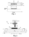
- the fiber 10 usually comprises silica, although other embodiments known in the art may comprise plastic compounds.
- the optical fiber 10 includes a core 12 and one or more claddings 14.
- the grating 20 is a series of periodic, aperiodic or pseudo-periodic variations on the core 12 and/or one or more of the claddings 14 of the fiber. As illustrated in the matched plot shown in Fig. 1, the grating 20 consists of variations in the refractive index of the fiber 10.
- FIG. 2 schematically illustrates an index writing assembly 100 using the writing method of the present invention.
- the index writing assembly 100 includes a source of light 130 producing a beam 132, an interference pattern generator 140, a modulator 150, and a fiber holding assembly 160 used to hold a fiber 110. More than one waveguide may be placed and translated simultaneously in the index writing assembly. Germanium or other photosensitive dopants are added to the silica glass of a region of the fiber 110, making the refractive index of that region of the optical fiber susceptible to change, generally an increase, upon exposure to actinic radiation. Commercially available photosensitive fibers, such as Corning® SMF-28 TM CPC6 (Corning Incorporated, Corning, NY), may be used. As those skilled in the art may appreciate, the method of the present invention also may be used to modify the refractive index not only of optical fibers, but also of other waveguides, such as planar waveguides.
- the light source 130 is a source of actinic radiation, such as a UV laser light or X-ray radiation.
- the source of light is selected to deliver a beam of sufficient intensity and having a sufficiently narrow diameter to write the desired grating.
- Other sources of light known in the art may be used depending on the type of fiber used and the desired grating pattern.
- the source of light 130 produces a beam 132 having a peak intensity of I 0 and a diameter D
- the interference pattern generator 140 is positioned between the fiber 110 and the source of light 130 and creates an intensity distribution, i.e. a spatially varying repeating light intensity pattern, which can be periodic or quasi-periodic (such as, for example, an interferogram), with a spatial period or pitch ⁇ 0 .
- the period ⁇ 0 of the intensity distribution generally matches the desired grating pitch.
- the interferogram may be produced by other methods, such as an interferometer.
- the periodic (or quasi-periodic) intensity distribution of actinic radiation used to fabricate a grating need not necessarily be obtained by constructing an interferdgram.
- an image reduction system utilizing amplitude masks may be used to create the intensity distribution.
- FIG. 3 illustrates schematically one embodiment of the electronic signal controls of modulator 150.
- the electronic signal controls of modulator 150 include an amplitude modulation function 152, a frequency modulation function 154 and a d.c. offset 156.
- a variety of modulators may be used, such as an opto-acoustic modulator (for example, IntraAction ASM-1251LA3 from IntraAction, Bellwood, IL).
- the modulator 150 amplitude modulates the beam 132 at a frequency f(t) .
- the electronic signal that controls the modulator may be shaped by a function generator, such as a Stanford Research Systems DSM345 (Stanford Research Systems, Sunnyvale, CA), to tailor the index perturbation profile along the fiber length to cause chirp and apodization in the resulting grating.
- a function generator such as a Stanford Research Systems DSM345 (Stanford Research Systems, Sunnyvale, CA) to tailor the index perturbation profile along the fiber length to cause chirp and apodization in the resulting grating.
- the fiber 110 is translated at a velocity ⁇ (t) relative to the intensity distribution. More than one waveguide may be translated simultaneously through the periodic intensity distribution. A laser beam that is amplitude-modulated as a function of time and a phase mask is used to create FBGs of any desired length.
- both f(t) and ⁇ (t) may be variable functions, or either or both could be constants.
- the term constant is defined within the acceptable parameters for deviations in the fiber grating pitch ( ⁇ ) due to jitter or error, as explained below.
- the movement of the fiber 110 in relation to the intensity distribution is controlled precisely by a translation mechanism.
- the fiber 110 is mounted on the fiber holding assembly 160, a very precise velocity-controlled motion stage which may be a rotary or linear stage.
- a continuous length of fiber is spooled in a spool 170 and the position of the writing beam is tracked to stay on the fiber as the spool rotates.
- the movement of the stage or the spool is coupled to act in synchrony with the modulator, ⁇ (t) / f(t) ⁇ ⁇ 0 .
- the translation mechanism may control the movement of the source of light 130 and of the interferogram generator 140.
- the laser beam 132 need not move relative to the phase mask 140.
- the fluence ⁇ (x) delivered to a given point of the waveguide can be expressed as where I 0 is the peak intensity illuminating the fiber and D is the diameter of the beam and ⁇ (x).
- a chirped FBG of any length may be manufactured.
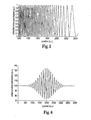
- Figure 5 illustrates an exemplary chirped refractive index profile of a fiber manufactured in accordance with the present invention.
- a small phase mask say 1" o.d.
- the dispersion compensation product covers the full Erbium-doped fiber amplifier range, from 1528 nm to 1568 nm.
- a 40 nm chirp is written into a single FBG with a laser beam diameter less than ⁇ 10 ⁇ m, by keeping the argument in the sinc function in equation (6) less than ⁇ .
- a 4 nm chirped FBG may be written with a beam diameter less than ⁇ 100 ⁇ m. These diameters are mathematical upper limits. In practice, one would use beams with diameters less than half this size to write a usable fringe visibility into the grating.
- the tuning parameter in the sinc function of equation (6) will increase from zero and cause the amplitude of the cosine-function spatial-modulation to decrease. If these control parameters are changed too much, no net modulation will result.
- the amplitude decrease is proportional to the diameter of the laser beam, which can be focused to make wide wavelength chirps possible.
- the limits of the relationship f(t) / ⁇ (t) ⁇ 1 / ⁇ 0 are defined at the limit where a sufficient refractive index modulation is written into the waveguide to create an acceptable grating. Depending on the type and the precision of grating that is being written, this difference between the sides of the above equation could be, for example, as large as 10%.
- the velocity of the motion stage and the frequency of the modulator would vary ⁇ 0.01 % to achieve 0.15 nm accuracy in the Erbium-doped fiber amplifier wavelength range.
- Scanning velocities are typically ⁇ 1 mm/s when manufacturing dispersion compensation FBGs, so a motion stage with ⁇ 0.1 ⁇ m/s precision is needed. With this writing speed, a ⁇ 2 KHz modulation with ⁇ 0.2 Hz flutter is needed to produce gratings in the Erbium-doped fiber amplifier band.
- the fiber may be rolled onto spools 170, as illustrated in Figure 4, which rotate to translate a continuous length of fiber 172 in front of an interferogram created by a phase mask from a modulated laser beam 174.
- the spool 170 is part of a spool to spool system.
- the rotational speed of these spools is achieved with a spindle motor controlled by simple phase-lock-loop circuitry 176 to provide precise rim velocities.
- the beam 174 is kept on the fiber 172 by vertically translating the beam 174 sychronous to the rotation of the spool 170.
- the position of the writing beam 174 may be tracked, such as with a laser beam, to stay on the fiber 172 as the spool rotates.
- the uncoated fiber may be permanently affixed to the spool, and the spool with the grating may be packaged, thereby reducing fiber handling.
- the method of the present invention also may be used to produce apodized fiber Bragg gratings, having a refractive index profile as illustrated in Figure 6.
- Pure apodized gratings may be manufactured with the method of the present invention by modulating the amplitude of the sinusoidal signal, via another function generator or suitable electronics, as the fiber is translated through the interferogram. To achieve pure-apodization, the sinusoidal-function amplitude is controlled before an offset is applied.
- the peak intensity illuminating the fiber, I 0 , velocity of translation, ⁇ , and the offset of the oscillating index perturbation, A may also be controlled to tailor the refractive index profile of a grating. If the peak intensity, velocity, and offset are held constant as a function of time, the average flux delivered to the fiber is constant, i.e. ⁇ ( x ) ⁇ I 0 / 4. D / ⁇ , regardless of the level of amplitude modulation.
- Chirped FBGs with pure apodization can be manufactured in a one-step writing process, without special phase masks, attenuation optics, or controlled laser beam attenuation.
- a 4-nm-wide linearly-chirped FBG that is 160 cm long can be manufactured by translating a fiber at a velocity of 1 mm/s across a phase mask of period 1.0739 ⁇ m as the frequency of the laser beam modulation is linearly varied from 1859.98 to 1864.76 Hz (a 4.784033 Hz span). Since the grating will take 1600 s to write, a raised-sinusoid apodization may be achieved by amplitude modulating the function generator output by a 0.312 milliHertz sinusoid. Other amplitude modulation profiles may be used to tailor the FBG for specific applications.
- FIG. 7 illustrates the use of long-length fiber Bragg grating 210 in a dispersion compensator 200.
- the signal 280 suffers from chromatic dispersation after traveling down a significant length of fiber (usually in the order of hundreds of kilometers).
- the signal is coupled to a circulator 284, which directs the signal to the long-length chirped fiber Bragg grating 210.
- the spectrum of wavelengths of the signal are each reflected after traveling a different distance through the fiber Bragg grating. The additional travel distance recompresses the signal, feeding a dispersion compensated signal 282 to the circulator 284.
- Figure 8 is a flow diagram illustrative of a state of the art method for manufacturing in-line optical waveguide refractive index gratings of virtually any length.
- a writing beam of actinic radiation is provided.
- a photosensitive waveguide is provided and placed across the path of the writing beam. Then, the waveguide is translated relative to the writing beam at a velocity v(t).
- the intensity of the writing beam as a function of time is modulated at a frequency f(t), wherein ⁇ (t) / f(t) ⁇ ⁇ . If apodized gratings are desired, the intensity of the writing beam may be varied further to control the envelope of the refractive index perturbation.
- the method of the present invention offers the ability to write in-line optical waveguide refractive index gratings of virtually any length with complicated refractive index profiles.
- the availability of gratings longer than one meter allows for the first time the effective use of gratings in a variety of applications.
- the inventive method disclosed in the present document can be used to modify the refractive index not only of optical fiber, but also of planar waveguides.
Landscapes
- Physics & Mathematics (AREA)
- General Physics & Mathematics (AREA)
- Optics & Photonics (AREA)
- Engineering & Computer Science (AREA)
- Chemical & Material Sciences (AREA)
- Dispersion Chemistry (AREA)
- Manufacturing & Machinery (AREA)
- Microelectronics & Electronic Packaging (AREA)
- Optical Fibers, Optical Fiber Cores, And Optical Fiber Bundles (AREA)
- Diffracting Gratings Or Hologram Optical Elements (AREA)
- Optical Integrated Circuits (AREA)
Applications Claiming Priority (3)
| Application Number | Priority Date | Filing Date | Title |
|---|---|---|---|
| US942590 | 1992-09-09 | ||
| US08/942,590 US5912999A (en) | 1997-10-02 | 1997-10-02 | Method for fabrication of in-line optical waveguide index grating of any length |
| PCT/US1998/013916 WO1999018462A1 (en) | 1997-10-02 | 1998-07-02 | Method for fabrication of in-line optical waveguide refractive index gratings of any length |
Publications (2)
| Publication Number | Publication Date |
|---|---|
| EP1010025A1 EP1010025A1 (en) | 2000-06-21 |
| EP1010025B1 true EP1010025B1 (en) | 2003-10-01 |
Family
ID=25478324
Family Applications (1)
| Application Number | Title | Priority Date | Filing Date |
|---|---|---|---|
| EP98967002A Expired - Lifetime EP1010025B1 (en) | 1997-07-02 | 1998-07-02 | Method of manufacturing an in-line optical waveguide refractive index grating of any length |
Country Status (9)
| Country | Link |
|---|---|
| US (1) | US5912999A (enExample) |
| EP (1) | EP1010025B1 (enExample) |
| JP (1) | JP2001519540A (enExample) |
| KR (1) | KR100534497B1 (enExample) |
| AU (1) | AU2701699A (enExample) |
| CA (1) | CA2305274C (enExample) |
| DE (1) | DE69818688T2 (enExample) |
| TW (1) | TW409187B (enExample) |
| WO (1) | WO1999018462A1 (enExample) |
Families Citing this family (47)
| Publication number | Priority date | Publication date | Assignee | Title |
|---|---|---|---|---|
| GB9509874D0 (en) * | 1995-05-16 | 1995-07-12 | Univ Southampton | Optical waveguide grating |
| FR2764394B1 (fr) * | 1997-06-10 | 1999-08-06 | France Telecom | Banc de photoinscription pour la realisation de reseaux de bragg |
| GB9722549D0 (en) * | 1997-10-24 | 1997-12-24 | Univ Southampton | Fabricating optical waveguide gratings and/or characterising optical waveguides |
| US6084995A (en) * | 1997-12-19 | 2000-07-04 | Nortel Networks Corporation | Reducing scanning errors |
| US6130973A (en) * | 1998-03-26 | 2000-10-10 | Institut National D'optique | Method and apparatus for spectrally designing all-fiber filters |
| CA2241707C (en) * | 1998-06-26 | 2002-04-02 | Mark Farries | Optical drop circuit having group delay compensation |
| KR100322121B1 (ko) | 1998-10-13 | 2002-03-08 | 윤종용 | 장주기격자필터제조장치 |
| US6163638A (en) * | 1998-10-29 | 2000-12-19 | Lucent Technologies Inc. | Article comprising an optical pulse compressor |
| GB2352529B (en) * | 1999-05-05 | 2003-04-23 | Furukawa Electric Europ Ltd | Optic fibre grating manufactured using phase mask and variable filter |
| KR100334812B1 (ko) | 1999-07-02 | 2002-05-02 | 윤종용 | 아포다이즈드 광섬유 격자 제작장치 |
| US6882477B1 (en) | 1999-11-10 | 2005-04-19 | Massachusetts Institute Of Technology | Method and system for interference lithography utilizing phase-locked scanning beams |
| IT1311335B1 (it) * | 1999-12-21 | 2002-03-12 | Otc Optical Technologies Ct S | Procedimento e dispositivo per realizzare reticoli in fibra ottica. |
| US6795636B1 (en) | 2000-03-05 | 2004-09-21 | 3M Innovative Properties Company | Radiation-transmissive films on glass articles |
| US6696157B1 (en) | 2000-03-05 | 2004-02-24 | 3M Innovative Properties Company | Diamond-like glass thin films |
| US6553163B2 (en) * | 2000-03-30 | 2003-04-22 | Corning, Incorporated | Method and apparatus for writing a Bragg grating in a waveguide |
| US6466703B1 (en) | 2000-04-07 | 2002-10-15 | Hrl Laboratories, Llc | Method and apparatus for electro-optic delay generation of optical signals |
| US6834134B2 (en) * | 2000-04-11 | 2004-12-21 | 3M Innovative Properties Company | Method and apparatus for generating frequency modulated pulses |
| WO2001090789A2 (en) * | 2000-05-22 | 2001-11-29 | Adc Telecommunications, Inc. | Polarization control of uv writing |
| EP1158088A3 (de) * | 2000-05-26 | 2003-01-22 | Voith Paper Patent GmbH | Verfahren und Vorrichtung zur Behandlung einer Faserstoffsuspension |
| KR100342532B1 (ko) * | 2000-08-04 | 2002-06-28 | 윤종용 | 편광 무의존성 장주기 광섬유 격자 제조 장치 |
| US6483965B1 (en) * | 2000-08-11 | 2002-11-19 | Nortel Networks Limited | Method of writing a bragg diffraction grating |
| US6591039B2 (en) * | 2000-11-16 | 2003-07-08 | Corning Oil Spa | Method and equipment for writing a Bragg grating in a waveguide |
| JP3813059B2 (ja) * | 2000-12-26 | 2006-08-23 | 三菱電機株式会社 | グレーティングの作製方法 |
| WO2002054631A2 (en) | 2000-12-30 | 2002-07-11 | University Of Rochester | Device and method for compensating for chromatic dispersion |
| US6898350B2 (en) * | 2001-01-18 | 2005-05-24 | General Dynamics Advanced Information Systems, Inc. | Interferometric focusing technique for forming taps in fibers |
| FR2825150B1 (fr) * | 2001-05-28 | 2003-09-26 | Univ Jean Monnet | Dispositif de caracterisation de reseaux optiques et procede de fabrication de reseaux optiques avec une frequence spatiale predefinie |
| JP3754634B2 (ja) * | 2001-06-27 | 2006-03-15 | 独立行政法人科学技術振興機構 | 光ファイバーグレーティングの作製方法及び作製装置、光ファイバーグレーティング |
| CA2354211A1 (en) * | 2001-07-26 | 2003-01-26 | Paul Lefebvre | Reel to reel manufacturing line |
| US20030059195A1 (en) * | 2001-08-29 | 2003-03-27 | Brennan James F. | Optical devices using shaped optical fibers and methods for making optical devices with shaped optical fibers |
| US6842544B2 (en) * | 2001-09-14 | 2005-01-11 | E. I. Du Pont De Nemours And Company | Method for apodizing a planar waveguide grating |
| US6882776B2 (en) | 2001-11-06 | 2005-04-19 | Intel Corporation | Method and apparatus of a semiconductor-based gain equalization device for optical amplifiers |
| US6859567B2 (en) * | 2001-11-30 | 2005-02-22 | Photintech Inc. | In-guide control of optical propagation |
| US6873762B1 (en) | 2002-04-08 | 2005-03-29 | The United States Of America As Represented By The Administrator Of The National Aeronautics And Space Administration | Fabrication of fiber optic grating apparatus and method |
| US6904202B1 (en) * | 2002-07-31 | 2005-06-07 | Intel Corporation | Writing waveguides with an arbitrary Bragg wavelength |
| US7277604B2 (en) * | 2003-12-12 | 2007-10-02 | Lxsix Photonics Inc. | Method and apparatus for inducing an index of refraction change on a substrate sensitive to electromagnetic radiation |
| US7432517B2 (en) * | 2004-11-19 | 2008-10-07 | Asml Netherlands B.V. | Pulse modifier, lithographic apparatus, and device manufacturing method |
| US7430376B1 (en) | 2004-11-29 | 2008-09-30 | Hrl Laboratories, Llc | All-optical delay generator for PPM communication systems based on a non-linear waveguide with a chirped DBR |
| US7085450B2 (en) * | 2004-12-22 | 2006-08-01 | 3M Innovative Properties Company | Fabrication of structures in an optical substrate |
| WO2008037089A1 (en) * | 2006-09-28 | 2008-04-03 | Universite Laval | System and method for permanently writing a diffraction grating in a low phonon energy glass medium |
| US7414547B2 (en) * | 2006-12-22 | 2008-08-19 | 3M Innovative Properties Company | Method and system for calibrating a rotary encoder and making a high resolution rotary encoder |
| DE102007035911A1 (de) * | 2007-07-27 | 2009-01-29 | Fraunhofer-Gesellschaft zur Förderung der angewandten Forschung e.V. | Verfahren und Vorrichtung zum Herstellen eines Gitters mit Chirp |
| US8828624B2 (en) * | 2009-08-03 | 2014-09-09 | Ipg Photonics Corporation | Method and device for fabricating volume Bragg gratings |
| US9405061B2 (en) * | 2012-08-08 | 2016-08-02 | Ofs Fitel, Llc | Avoiding beam obstruction during inscription of fiber gratings |
| US9568670B2 (en) * | 2013-02-21 | 2017-02-14 | Ofs Fitel, Llc | Index matched grating inscription |
| CN112764145A (zh) * | 2021-02-01 | 2021-05-07 | 西安交通大学 | 一种基于时序控制的二维光栅高效制造方法 |
| CN114265142B (zh) * | 2021-12-17 | 2023-07-18 | 中国科学院上海光学精密机械研究所 | 一种提高超窄带光纤光栅边模抑制比和光谱矩形度的方法 |
| CN114706152B (zh) * | 2022-03-15 | 2023-06-20 | 清华大学 | 图案化闪耀光栅的加工方法及系统 |
Family Cites Families (5)
| Publication number | Priority date | Publication date | Assignee | Title |
|---|---|---|---|---|
| US5066133A (en) * | 1990-10-18 | 1991-11-19 | United Technologies Corporation | Extended length embedded Bragg grating manufacturing method and arrangement |
| US5363239A (en) * | 1992-12-23 | 1994-11-08 | At&T Bell Laboratories | Method for forming spatially-varying distributed Bragg reflectors in optical media |
| GB2289771B (en) * | 1994-05-26 | 1997-07-30 | Northern Telecom Ltd | Forming Bragg gratings in photosensitive waveguides |
| US5708738A (en) * | 1996-03-05 | 1998-01-13 | The United States Of America As Represented By The Secretary Of The Navy | Apparatus and process for making fiber optic bragg gratings |
| GB2316760A (en) * | 1996-08-23 | 1998-03-04 | Univ Southampton | Fabricating optical waveguide gratings |
-
1997
- 1997-10-02 US US08/942,590 patent/US5912999A/en not_active Expired - Lifetime
-
1998
- 1998-07-02 DE DE69818688T patent/DE69818688T2/de not_active Expired - Lifetime
- 1998-07-02 AU AU27016/99A patent/AU2701699A/en not_active Abandoned
- 1998-07-02 WO PCT/US1998/013916 patent/WO1999018462A1/en not_active Ceased
- 1998-07-02 KR KR10-2000-7003556A patent/KR100534497B1/ko not_active Expired - Lifetime
- 1998-07-02 EP EP98967002A patent/EP1010025B1/en not_active Expired - Lifetime
- 1998-07-02 CA CA002305274A patent/CA2305274C/en not_active Expired - Lifetime
- 1998-07-02 JP JP2000515197A patent/JP2001519540A/ja active Pending
- 1998-09-16 TW TW087115441A patent/TW409187B/zh not_active IP Right Cessation
Non-Patent Citations (1)
| Title |
|---|
| Electronics Letters, Vol.20, (1990), pages 1270-1272 * |
Also Published As
| Publication number | Publication date |
|---|---|
| AU2701699A (en) | 1999-04-27 |
| WO1999018462A1 (en) | 1999-04-15 |
| CA2305274A1 (en) | 1999-04-15 |
| TW409187B (en) | 2000-10-21 |
| JP2001519540A (ja) | 2001-10-23 |
| KR20010030865A (ko) | 2001-04-16 |
| EP1010025A1 (en) | 2000-06-21 |
| DE69818688D1 (de) | 2003-11-06 |
| KR100534497B1 (ko) | 2005-12-08 |
| US5912999A (en) | 1999-06-15 |
| DE69818688T2 (de) | 2004-08-05 |
| CA2305274C (en) | 2007-09-11 |
Similar Documents
| Publication | Publication Date | Title |
|---|---|---|
| EP1010025B1 (en) | Method of manufacturing an in-line optical waveguide refractive index grating of any length | |
| US6404956B1 (en) | Long-length continuous phase Bragg reflectors in optical media | |
| US6728444B2 (en) | Fabrication of chirped fiber bragg gratings of any desired bandwidth using frequency modulation | |
| AU748701B2 (en) | Method for writing arbitrary index perturbations on a waveguide | |
| Asseh et al. | A writing technique for long fiber Bragg gratings with complex reflectivity profiles | |
| US5604829A (en) | Optical waveguide with diffraction grating and method of forming the same | |
| EP0843186B1 (en) | Creation of Bragg reflective gratings in waveguides | |
| CA2236250C (en) | Creation of bragg reflective gratings in waveguides | |
| US5748814A (en) | Method for spatially controlling the period and amplitude of Bragg filters | |
| Melo et al. | Fabrication of tailored Bragg gratings by the phase mask dithering/moving technique | |
| US6574395B1 (en) | Photowritten Bragg grating apodization method | |
| US5953471A (en) | Optical communication system having short period reflective Bragg gratings | |
| US5903689A (en) | Method for spatially controlling the period and amplitude of BRAGG filters | |
| US5572609A (en) | Optical fiber vibration modal filter for flexible structures produced by the photorefractive effect | |
| WO1997010697A9 (en) | An optical fiber vibration modal filter for flexible structures produced by the photorefractive effect | |
| CA2640710C (en) | Apparatus and method for producing fibre bragg gratings in a waveguide | |
| Stubbe et al. | Novel technique for writing long superstructured fiber Bragg gratings | |
| EP1207410A1 (en) | Method and equipment for writing a bragg grating in a waveguide | |
| JP4279227B2 (ja) | 光導波路ブラッググレーティングの製造方法および製造装置 | |
| US20030059164A1 (en) | Grating error compensating technique | |
| Yoffe et al. | Flexible and stable interferometer for fabricating fiber Bragg gratings | |
| Kashyap et al. | Infinite length fibre gratings using circular amplitude and phase masks | |
| Arkwright et al. | A technique for accurately calibrating the motion of a phase mask used to inscribe complex fibre Bragg grating structures |
Legal Events
| Date | Code | Title | Description |
|---|---|---|---|
| PUAI | Public reference made under article 153(3) epc to a published international application that has entered the european phase |
Free format text: ORIGINAL CODE: 0009012 |
|
| 17P | Request for examination filed |
Effective date: 20000308 |
|
| AK | Designated contracting states |
Kind code of ref document: A1 Designated state(s): DE ES FR GB IT |
|
| 17Q | First examination report despatched |
Effective date: 20010515 |
|
| GRAH | Despatch of communication of intention to grant a patent |
Free format text: ORIGINAL CODE: EPIDOS IGRA |
|
| RTI1 | Title (correction) |
Free format text: METHOD OF MANUFACTURING AN IN-LINE OPTICAL WAVEGUIDE REFRACTIVE INDEX GRATING OF ANY LENGTH |
|
| GRAS | Grant fee paid |
Free format text: ORIGINAL CODE: EPIDOSNIGR3 |
|
| GRAA | (expected) grant |
Free format text: ORIGINAL CODE: 0009210 |
|
| AK | Designated contracting states |
Kind code of ref document: B1 Designated state(s): DE ES FR GB IT |
|
| PG25 | Lapsed in a contracting state [announced via postgrant information from national office to epo] |
Ref country code: IT Free format text: LAPSE BECAUSE OF FAILURE TO SUBMIT A TRANSLATION OF THE DESCRIPTION OR TO PAY THE FEE WITHIN THE PRE;WARNING: LAPSES OF ITALIAN PATENTS WITH EFFECTIVE DATE BEFORE 2007 MAY HAVE OCCURRED AT ANY TIME BEFORE 2007. THE CORRECT EFFECTIVE DATE MAY BE DIFFERENT FROM THE ONE RECORDED.SCRIBED TIME-LIMIT Effective date: 20031001 |
|
| REG | Reference to a national code |
Ref country code: GB Ref legal event code: FG4D |
|
| REF | Corresponds to: |
Ref document number: 69818688 Country of ref document: DE Date of ref document: 20031106 Kind code of ref document: P |
|
| PG25 | Lapsed in a contracting state [announced via postgrant information from national office to epo] |
Ref country code: ES Free format text: LAPSE BECAUSE OF FAILURE TO SUBMIT A TRANSLATION OF THE DESCRIPTION OR TO PAY THE FEE WITHIN THE PRESCRIBED TIME-LIMIT Effective date: 20040112 |
|
| ET | Fr: translation filed | ||
| PLBE | No opposition filed within time limit |
Free format text: ORIGINAL CODE: 0009261 |
|
| STAA | Information on the status of an ep patent application or granted ep patent |
Free format text: STATUS: NO OPPOSITION FILED WITHIN TIME LIMIT |
|
| 26N | No opposition filed |
Effective date: 20040702 |
|
| REG | Reference to a national code |
Ref country code: FR Ref legal event code: PLFP Year of fee payment: 19 |
|
| REG | Reference to a national code |
Ref country code: FR Ref legal event code: PLFP Year of fee payment: 20 |
|
| PGFP | Annual fee paid to national office [announced via postgrant information from national office to epo] |
Ref country code: FR Payment date: 20170613 Year of fee payment: 20 Ref country code: GB Payment date: 20170628 Year of fee payment: 20 |
|
| PGFP | Annual fee paid to national office [announced via postgrant information from national office to epo] |
Ref country code: DE Payment date: 20170627 Year of fee payment: 20 |
|
| REG | Reference to a national code |
Ref country code: DE Ref legal event code: R071 Ref document number: 69818688 Country of ref document: DE |
|
| REG | Reference to a national code |
Ref country code: GB Ref legal event code: PE20 Expiry date: 20180701 |
|
| PG25 | Lapsed in a contracting state [announced via postgrant information from national office to epo] |
Ref country code: GB Free format text: LAPSE BECAUSE OF EXPIRATION OF PROTECTION Effective date: 20180701 |