EP1006368A2 - Opto-elektronischer Sensor und Verfahren zu dessen Herstellung - Google Patents
Opto-elektronischer Sensor und Verfahren zu dessen Herstellung Download PDFInfo
- Publication number
- EP1006368A2 EP1006368A2 EP99119450A EP99119450A EP1006368A2 EP 1006368 A2 EP1006368 A2 EP 1006368A2 EP 99119450 A EP99119450 A EP 99119450A EP 99119450 A EP99119450 A EP 99119450A EP 1006368 A2 EP1006368 A2 EP 1006368A2
- Authority
- EP
- European Patent Office
- Prior art keywords
- injection
- housing
- electronic components
- sensor
- optical
- Prior art date
- Legal status (The legal status is an assumption and is not a legal conclusion. Google has not performed a legal analysis and makes no representation as to the accuracy of the status listed.)
- Withdrawn
Links
Images

Classifications
-
- G—PHYSICS
- G01—MEASURING; TESTING
- G01S—RADIO DIRECTION-FINDING; RADIO NAVIGATION; DETERMINING DISTANCE OR VELOCITY BY USE OF RADIO WAVES; LOCATING OR PRESENCE-DETECTING BY USE OF THE REFLECTION OR RERADIATION OF RADIO WAVES; ANALOGOUS ARRANGEMENTS USING OTHER WAVES
- G01S7/00—Details of systems according to groups G01S13/00, G01S15/00, G01S17/00
- G01S7/48—Details of systems according to groups G01S13/00, G01S15/00, G01S17/00 of systems according to group G01S17/00
- G01S7/481—Constructional features, e.g. arrangements of optical elements
- G01S7/4811—Constructional features, e.g. arrangements of optical elements common to transmitter and receiver
-
- G—PHYSICS
- G01—MEASURING; TESTING
- G01V—GEOPHYSICS; GRAVITATIONAL MEASUREMENTS; DETECTING MASSES OR OBJECTS; TAGS
- G01V8/00—Prospecting or detecting by optical means
- G01V8/10—Detecting, e.g. by using light barriers
Definitions
- the invention relates to an opto-electronic sensor with in a housing arranged optical and electronic components and a Method of manufacturing such a sensor.
- the plastic mass used for the housing and optical components is preferably at least partially transparent to visible light, UV radiation or infrared radiation, depending on the type of each to be manufactured Sensors.
- the stated property of the plastic mass enables the latter the imaging necessary for the realization of the optical components To give properties.
- the plastic mass for example be designed as an optical filter, so that they ultimately a Triple function as a lens, filter and housing can perform.
- the process according to the invention is preferably carried out in such a way that the electronic components before the injection or casting process on one Board arranged and then the board in a precise position Injection or casting tool is inserted, whereupon the injection or Casting process can take place.
- the positioning of the board in the spray or Casting tool can advantageously by provided in the board Positioning holes and associated positioning pins in the injection or casting tool can be simplified.
- these sensors can either be outside the injection or casting tool or be isolated within this tool, the latter If the separation is preferred by means of a punching process he follows.
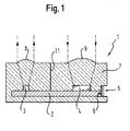
- Fig. 1 shows a sensor 1 with a flat, perpendicular to the plane of the drawing extending circuit board 2, arranged on the electronic components are. These electronic components are shown in FIG. 1 For the sake of clarity, only one light transmitter 3 and one light receiver 4 drawn. Other electronic components can also be found on the board 2, but are not shown in Fig. 1.
- a socket 6 is provided on a narrow side 5 of the circuit board 2, via which the sensor 1 with supply, control and / or data lines can be coupled.
- the socket 6 could for example also on the Bottom of the board 2 may be provided.
- Fig. 2a shows a flat element - often referred to as "benefit" 10, which comprises a plurality of boards 2.
- 2a are exemplary only three boards 2 drawn.
- Each board 2 carries all electronic Components that are necessary to implement a single sensor.
- the individual boards 2 are in the flat element 10 via thin webs 12 held so that between the flat element 10 and the boards 2, an air gap 13 is formed, which apart from minor interruptions through the webs 12 almost over the full extent of the respective boards 2 extends.
- This air gap 13 makes an almost complete one Injection molding or casting around the boards 2 possible.
- the boards 2 are thus with one another via the webs 12 and the element 10 connected within a common plane and relative to each other unchangeably adjusted.
- each Cavity has the negative form of a sensor to be manufactured including the negative form of the optical components to be formed.
- the individual sensors can 1 separated from each other by means of a suitable work step as shown in Fig. 2c.
Landscapes
- Physics & Mathematics (AREA)
- General Physics & Mathematics (AREA)
- Engineering & Computer Science (AREA)
- Life Sciences & Earth Sciences (AREA)
- General Life Sciences & Earth Sciences (AREA)
- Geophysics (AREA)
- Computer Networks & Wireless Communication (AREA)
- Radar, Positioning & Navigation (AREA)
- Remote Sensing (AREA)
- Casting Or Compression Moulding Of Plastics Or The Like (AREA)
- Geophysics And Detection Of Objects (AREA)
- Light Receiving Elements (AREA)
Abstract
Description
- Zur Herstellung von flüssigkeits- oder gasdichten Sensoren ist es nicht mehr nötig, die optischen Bauteile gegenüber dem Gehäuse abzudichten, da diese optischen Bauteile und das Gehäuse einstückig aus einer einheitlichen Kunststoffmasse geformt sind.
- Zwischen einem Lichtsender bzw. einem Lichtempfänger und dem Gehäuse ist ein besonders guter Wärmeübergang gegeben, da die Kunststoffmasse zum einen direkt am Lichtsender bzw. Lichtempfänger und zum anderen direkt am Gehäuse anliegen kann, so daß die Kunststoffmasse Wärme von Lichtsender bzw. Lichtempfänger zur Gehäuseoberfläche leiten kann, ohne daß zwischen den genannten Bauteilen störende Luftspalte vorhanden wären.
- Positionierungs- und Justierungsungenauigkeiten zwischen optischen Bauteilen und Gehäuse werden ausgeschlossen, da die Relativposition von optischen Bauteilen und Gehäuse durch die Gestalt des Spritz- bzw. Gießwerkzeugs fest und unveränderlich vorgegeben ist.
- Fig. 1
- einen Schnitt durch einen erfindungsgemäßen Sensor und
- Fig. 2a-c
- drei Verfahrensschritte bei der gleichzeitigen Herstellung mehrerer Sensoren.
- 1
- Sensor
- 2
- Platine
- 3
- Lichtsender
- 4
- Lichtempfänger
- 5
- Platinenschmalseite
- 6
- Buchse
- 7
- Kunststoffmasse
- 8
- Sendeoptik
- 9
- Empfangsoptik
- 10
- Flächenelement
- 11
- Trennplatte
- 12
- Stege
- 13
- Luftspalte
Claims (12)
- Opto-elektronischer Sensor (1) mit in einem Gehäuse angeordneten optischen und elektronischen Bauteilen (3, 4, 8, 9),
dadurch gekennzeichnet,
daß sowohl das Gehäuse als auch die optischen Bauteile (8, 9) aus einer einheitlichen Kunststoffmasse (7) gebildet sind, welche die elektronischen Bauteile (3, 4) einbettend umschließt. - Sensor nach Anspruch 1,
dadurch gekennzeichnet,
daß die Kunststoffmasse (7) für sichtbares Licht, UV-Strahlung oder Infrarotstrahlung zumindest teilweise durchlässig und insbesondere als optisches Filter ausgebildet ist. - Sensor nach einem der vorhergehenden Ansprüche,
dadurch gekennzeichnet,
daß das Gehäuse und die optischen Bauteile (8, 9) durch einen einzigen, gemeinsamen Spritz- oder Gießvorgang gebildet sind. - Sensor nach einem der vorhergehenden Ansprüche,
dadurch gekennzeichnet,
daß die Kunststoffmasse (7) unmittelbar, ohne Ausbildung eines Luftspalts an einen Lichtsender (3) und/oder einen Lichtempfänger (4) angrenzt. - Sensor nach einem der vorhergehenden Ansprüche,
dadurch gekennzeichnet,
daß die elektronischen Bauteile (3, 4) mit einem Kabel, einem Stecker und/oder einer Buchse (6) gekoppelt sind. - Sensor nach Anspruch 5,
dadurch gekennzeichnet,
daß Kabel, Stecker und/oder Buchse (6) zumindest teilweise in der Kunststoffmasse (7) eingebettet sind. - Verfahren zur Herstellung eines opto-elektronischen Sensors (1) mit in einem Gehäuse angeordneten optischen und elektronischen Bauteilen (3, 4, 8, 9),
dadurch gekennzeichnet,
daß sowohl das Gehäuse als auch die optischen Bauteile (8, 9) durch einen einzigen, gemeinsamen Spritz- oder Gießvorgang aus einer einheitlichen Kunststoffmasse (7) gefertigt werden, wobei die elektronischen Bauteile (3, 4) mittels des Spritz- oder Gießvorgangs in der Kunststoffmasse (7) eingebettet werden. - Verfahren nach Anspruch 7,
dadurch gekennzeichnet,
daß das Spritz- oder Gießwerkzeug unter anderem die Negativform der zu bildenden optischen Bauteile (8, 9) aufweist. - Verfahren nach einem der Ansprüche 7 oder 8,
dadurch gekennzeichnet,
daß die insbesondere auf einer Platine (2) angeordneten elektronischen Bauteile (3, 4) vor dem Spritz- oder Gießvorgang positionsgenau in einem Spritz- oder Gießwerkzeug angeordnet werden, woraufhin der Spritz- oder Gießvorgang erfolgt. - Verfahren nach einem der Ansprüche 7 bis 9,
dadurch gekennzeichnet,
daß zur gleichzeitigen Herstellung einer Mehrzahl von Sensoren (1) mehrere, miteinander verbundene, jeweils einem Sensor (1) zugeordnete Platinen (2) in einem einzigen Verfahrensschritt mit Kunststoffmasse (7) umspritzt oder umgossen werden. - Verfahren nach Anspruch 10,
dadurch gekennzeichnet,
daß die Sensoren (1) im Spritz- oder Gießwerkzeug insbesondere mittels eines Stanzvorgangs vereinzelt werden. - Verfahren nach Anspruch 10,
dadurch gekennzeichnet,
daß die Sensoren (1) außerhalb des Spritz- oder Gießwerkzeugs vereinzelt werden.
Applications Claiming Priority (2)
| Application Number | Priority Date | Filing Date | Title |
|---|---|---|---|
| DE19855220 | 1998-11-30 | ||
| DE1998155220 DE19855220A1 (de) | 1998-11-30 | 1998-11-30 | Opto-elektronischer Sensor und Verfahren zu dessen Herstellung |
Publications (2)
| Publication Number | Publication Date |
|---|---|
| EP1006368A2 true EP1006368A2 (de) | 2000-06-07 |
| EP1006368A3 EP1006368A3 (de) | 2001-10-04 |
Family
ID=7889510
Family Applications (1)
| Application Number | Title | Priority Date | Filing Date |
|---|---|---|---|
| EP99119450A Withdrawn EP1006368A3 (de) | 1998-11-30 | 1999-09-30 | Opto-elektronischer Sensor und Verfahren zu dessen Herstellung |
Country Status (2)
| Country | Link |
|---|---|
| EP (1) | EP1006368A3 (de) |
| DE (1) | DE19855220A1 (de) |
Cited By (3)
| Publication number | Priority date | Publication date | Assignee | Title |
|---|---|---|---|---|
| EP1293761A1 (de) * | 2001-09-07 | 2003-03-19 | Leopold Kostal GmbH & Co. KG | Optoelektronischer Sensor, Verwendung eines solchen Sensors sowie optoelektronischer Lenkwinkelsensor |
| EP1376065A3 (de) * | 2002-06-28 | 2004-10-27 | Stegmann GmbH & Co. KG | Optoelektronisches Winkelmessgerät sowie Verfahren zu dessen Herstellung |
| WO2007028667A1 (de) * | 2005-09-05 | 2007-03-15 | Robert Bosch Gmbh | Elektro-optisches messgerät |
Families Citing this family (4)
| Publication number | Priority date | Publication date | Assignee | Title |
|---|---|---|---|---|
| DE10308285A1 (de) | 2003-02-26 | 2004-09-09 | Sick Ag | Optische Sende- und Empfangsanordnung |
| DE102009046872B4 (de) | 2009-11-19 | 2018-06-21 | Ifm Electronic Gmbh | Berührungslos arbeitendes elektronisches Schaltgerät mit einer optischen Schaltzustandsanzeige |
| WO2012170006A1 (en) * | 2011-06-06 | 2012-12-13 | Next Holdings Limited | Simplified optical position sensing assembly |
| DE102013007961B4 (de) * | 2013-05-10 | 2023-06-22 | Audi Ag | Optisches Messsystem für ein Fahrzeug |
Family Cites Families (13)
| Publication number | Priority date | Publication date | Assignee | Title |
|---|---|---|---|---|
| US3697762A (en) * | 1970-12-14 | 1972-10-10 | Philips Corp | Photo electric switching device |
| DE2247717A1 (de) * | 1972-09-28 | 1974-05-02 | Siemens Ag | Lichtschranke |
| US4878107A (en) * | 1985-10-29 | 1989-10-31 | Hopper William R | Touch sensitive indicating light |
| JPS63176A (ja) * | 1986-06-19 | 1988-01-05 | Honda Motor Co Ltd | 複合型光センサ |
| DE3643842C2 (de) * | 1986-12-20 | 1995-07-20 | Leuze Electronic Gmbh & Co | Anordnung zur berührungslosen Bestimmung der räumlichen Lage eines auf der Oberfläche eines Körpers befindlichen Objektpunkts |
| DE4113720C2 (de) * | 1991-04-26 | 1996-01-11 | Daimler Benz Ag | Gabellichtschranke |
| DE4225512C1 (de) * | 1992-08-01 | 1994-02-17 | Bosch Gmbh Robert | Optoelektronischer Strahlungsempfänger |
| DE4304545C2 (de) * | 1993-02-11 | 1998-10-01 | Felten & Guilleaume Energie | Kabel mit Lichtwellenleitern |
| US5506445A (en) * | 1994-06-24 | 1996-04-09 | Hewlett-Packard Company | Optical transceiver module |
| US5528474A (en) * | 1994-07-18 | 1996-06-18 | Grote Industries, Inc. | Led array vehicle lamp |
| DE4439838C2 (de) * | 1994-11-08 | 1999-02-25 | Telefunken Microelectron | Gabelkoppler |
| DE19535777A1 (de) * | 1995-09-26 | 1997-03-27 | Siemens Ag | Optoelektronisches Halbleiter-Bauelement und Verfahren zur Herstellung |
| DE19718157A1 (de) * | 1997-04-29 | 1998-11-05 | Sick Ag | Opto-elektronischer Sensor |
-
1998
- 1998-11-30 DE DE1998155220 patent/DE19855220A1/de not_active Withdrawn
-
1999
- 1999-09-30 EP EP99119450A patent/EP1006368A3/de not_active Withdrawn
Cited By (6)
| Publication number | Priority date | Publication date | Assignee | Title |
|---|---|---|---|---|
| EP1293761A1 (de) * | 2001-09-07 | 2003-03-19 | Leopold Kostal GmbH & Co. KG | Optoelektronischer Sensor, Verwendung eines solchen Sensors sowie optoelektronischer Lenkwinkelsensor |
| EP1376065A3 (de) * | 2002-06-28 | 2004-10-27 | Stegmann GmbH & Co. KG | Optoelektronisches Winkelmessgerät sowie Verfahren zu dessen Herstellung |
| US7012677B2 (en) | 2002-06-28 | 2006-03-14 | Stegman Gmbh & Co. Kg | Optoelectronic angle measuring instrument and method for its production |
| WO2007028667A1 (de) * | 2005-09-05 | 2007-03-15 | Robert Bosch Gmbh | Elektro-optisches messgerät |
| US7796250B2 (en) | 2005-09-05 | 2010-09-14 | Robert Bosch Gmbh | Electro-optical measuring device |
| CN101258419B (zh) * | 2005-09-05 | 2013-03-13 | 罗伯特·博世有限公司 | 光电的测量仪器 |
Also Published As
| Publication number | Publication date |
|---|---|
| DE19855220A1 (de) | 2000-05-31 |
| EP1006368A3 (de) | 2001-10-04 |
Similar Documents
| Publication | Publication Date | Title |
|---|---|---|
| DE102007044555A1 (de) | Optische Koppelvorrichtung und Verfahren zu deren Herstellung | |
| EP1252540B1 (de) | Optisches sende-/empfangsmodul mit internem lichtwellenleiter | |
| DE69833150T2 (de) | Vorrichtung zur Herstellung einer faseroptischen Steckerferrule | |
| DE69107326T2 (de) | Integriert optische Komponente und Verfahren ihrer Herstellung. | |
| DE10049356B4 (de) | Halbleitersensor | |
| EP1187227A2 (de) | Oberflächenmontierbares Opto-Bauelement und Verfahren zum Herstellen desselben | |
| DE4428158A1 (de) | Optoelektronisches Interfacemodul und Verfahren zu dessen Herstellung | |
| DE2648652B2 (de) | Verbindungselement für optische Fasern | |
| EP1031860A2 (de) | Verfahren und Gissform zum Herstellen eines elektrooptischen Moduls und elektrooptisches Modul | |
| DE10015950A1 (de) | Steckerbuchse, Herstellungsverfahren derselben und einen die Steckerbuchse aufnehmenden optischer Steckverbinder | |
| DE10223946A1 (de) | Drehdetektoreinrichtung und Verfahren zu deren Herstellung | |
| DE69311291T2 (de) | Modulare optische Wellenleiterstruktur | |
| DE102008012584A1 (de) | Elektronische Vorrichtung mit einem geformten Harzgehäuse, und Formungswerkzeug und Verfahren zur Herstellung desselben | |
| DE60119424T2 (de) | Methode zur Herstellung einer faseroptischen Steckerferrule | |
| EP0462362A2 (de) | Optische Verbindung für Lichtwellenleiter | |
| DE69837129T2 (de) | Faseroptischer Steckerstift | |
| EP1006368A2 (de) | Opto-elektronischer Sensor und Verfahren zu dessen Herstellung | |
| DE69834870T2 (de) | Ausrichtsystem für einen faseroptischen Steckerstift | |
| EP2265102A1 (de) | Sensoraufbau ohne Gehäuse | |
| DE2924068C2 (de) | Verfahren zur Herstellung koplanarer optoelektronischer Koppelelemente | |
| EP0043475B1 (de) | Verfahren zur Herstellung einer integrierten mikrooptischen Vorrichtung zur Verwendung mit Multimode-Lichtfasern | |
| DE69108606T2 (de) | Herstellungsverfahren von einem Eingangskonns an einem faseroptischen Steckerstift und Vorrichtung zu dessen Durchführung. | |
| EP0236712B1 (de) | Verfahren zum positionsgerechten Fügen von Lichtwellenleitern in Koppelstellen und Koppelelement für Lichtwellenleiter-Schalter | |
| DE4224618A1 (de) | Verfahren zum Herstellen elektrischer Steckverbindungen und nach dem Verfahren hergestellte Steckverbindung | |
| EP1018051B1 (de) | Verfahren zum herstellen eines optoelektronischen steckeraufnahmeelementes und optoelektronischer stecker |
Legal Events
| Date | Code | Title | Description |
|---|---|---|---|
| PUAI | Public reference made under article 153(3) epc to a published international application that has entered the european phase |
Free format text: ORIGINAL CODE: 0009012 |
|
| AK | Designated contracting states |
Kind code of ref document: A2 Designated state(s): AT BE CH CY DE DK ES FI FR GB GR IE IT LI LU MC NL PT SE |
|
| AX | Request for extension of the european patent |
Free format text: AL;LT;LV;MK;RO;SI |
|
| PUAL | Search report despatched |
Free format text: ORIGINAL CODE: 0009013 |
|
| AK | Designated contracting states |
Kind code of ref document: A3 Designated state(s): AT BE CH CY DE DK ES FI FR GB GR IE IT LI LU MC NL PT SE |
|
| AX | Request for extension of the european patent |
Free format text: AL;LT;LV;MK;RO;SI |
|
| RIC1 | Information provided on ipc code assigned before grant |
Free format text: 7G 01S 7/481 A, 7H 05K 1/18 B, 7H 01L 31/0203 B |
|
| AKX | Designation fees paid | ||
| REG | Reference to a national code |
Ref country code: DE Ref legal event code: 8566 |
|
| STAA | Information on the status of an ep patent application or granted ep patent |
Free format text: STATUS: THE APPLICATION IS DEEMED TO BE WITHDRAWN |
|
| 18D | Application deemed to be withdrawn |
Effective date: 20020405 |