EP1003281B1 - Multi-input differential amplifier circuit - Google Patents
Multi-input differential amplifier circuit Download PDFInfo
- Publication number
- EP1003281B1 EP1003281B1 EP99402874A EP99402874A EP1003281B1 EP 1003281 B1 EP1003281 B1 EP 1003281B1 EP 99402874 A EP99402874 A EP 99402874A EP 99402874 A EP99402874 A EP 99402874A EP 1003281 B1 EP1003281 B1 EP 1003281B1
- Authority
- EP
- European Patent Office
- Prior art keywords
- input
- circuit
- amplifier circuit
- transistors
- differential amplifier
- Prior art date
- Legal status (The legal status is an assumption and is not a legal conclusion. Google has not performed a legal analysis and makes no representation as to the accuracy of the status listed.)
- Expired - Lifetime
Links
Images


Classifications
-
- H—ELECTRICITY
- H03—ELECTRONIC CIRCUITRY
- H03F—AMPLIFIERS
- H03F3/00—Amplifiers with only discharge tubes or only semiconductor devices as amplifying elements
- H03F3/45—Differential amplifiers
- H03F3/45071—Differential amplifiers with semiconductor devices only
- H03F3/45076—Differential amplifiers with semiconductor devices only characterised by the way of implementation of the active amplifying circuit in the differential amplifier
- H03F3/45179—Differential amplifiers with semiconductor devices only characterised by the way of implementation of the active amplifying circuit in the differential amplifier using MOSFET transistors as the active amplifying circuit
- H03F3/45183—Long tailed pairs
-
- H—ELECTRICITY
- H03—ELECTRONIC CIRCUITRY
- H03F—AMPLIFIERS
- H03F2203/00—Indexing scheme relating to amplifiers with only discharge tubes or only semiconductor devices as amplifying elements covered by H03F3/00
- H03F2203/45—Indexing scheme relating to differential amplifiers
- H03F2203/45361—Indexing scheme relating to differential amplifiers the AAC comprising multiple transistors parallel coupled at their drains only, e.g. in a cascode dif amp, only those forming the composite common source transistor
-
- H—ELECTRICITY
- H03—ELECTRONIC CIRCUITRY
- H03F—AMPLIFIERS
- H03F2203/00—Indexing scheme relating to amplifiers with only discharge tubes or only semiconductor devices as amplifying elements covered by H03F3/00
- H03F2203/45—Indexing scheme relating to differential amplifiers
- H03F2203/45382—Indexing scheme relating to differential amplifiers the AAC comprising common gate stages in the source circuit of the AAC before the common source coupling
-
- H—ELECTRICITY
- H03—ELECTRONIC CIRCUITRY
- H03F—AMPLIFIERS
- H03F2203/00—Indexing scheme relating to amplifiers with only discharge tubes or only semiconductor devices as amplifying elements covered by H03F3/00
- H03F2203/45—Indexing scheme relating to differential amplifiers
- H03F2203/45392—Indexing scheme relating to differential amplifiers the AAC comprising resistors in the source circuit of the AAC before the common source coupling
-
- H—ELECTRICITY
- H03—ELECTRONIC CIRCUITRY
- H03F—AMPLIFIERS
- H03F2203/00—Indexing scheme relating to amplifiers with only discharge tubes or only semiconductor devices as amplifying elements covered by H03F3/00
- H03F2203/45—Indexing scheme relating to differential amplifiers
- H03F2203/45616—Indexing scheme relating to differential amplifiers the IC comprising more than one switch, which are not cross coupled
-
- H—ELECTRICITY
- H03—ELECTRONIC CIRCUITRY
- H03F—AMPLIFIERS
- H03F2203/00—Indexing scheme relating to amplifiers with only discharge tubes or only semiconductor devices as amplifying elements covered by H03F3/00
- H03F2203/45—Indexing scheme relating to differential amplifiers
- H03F2203/45664—Indexing scheme relating to differential amplifiers the LC comprising one or more cascaded inverter stages as output stage at one output of the dif amp circuit
-
- H—ELECTRICITY
- H03—ELECTRONIC CIRCUITRY
- H03F—AMPLIFIERS
- H03F2203/00—Indexing scheme relating to amplifiers with only discharge tubes or only semiconductor devices as amplifying elements covered by H03F3/00
- H03F2203/45—Indexing scheme relating to differential amplifiers
- H03F2203/45674—Indexing scheme relating to differential amplifiers the LC comprising one current mirror
-
- H—ELECTRICITY
- H03—ELECTRONIC CIRCUITRY
- H03F—AMPLIFIERS
- H03F2203/00—Indexing scheme relating to amplifiers with only discharge tubes or only semiconductor devices as amplifying elements covered by H03F3/00
- H03F2203/45—Indexing scheme relating to differential amplifiers
- H03F2203/45702—Indexing scheme relating to differential amplifiers the LC comprising two resistors
-
- H—ELECTRICITY
- H03—ELECTRONIC CIRCUITRY
- H03F—AMPLIFIERS
- H03F2203/00—Indexing scheme relating to amplifiers with only discharge tubes or only semiconductor devices as amplifying elements covered by H03F3/00
- H03F2203/45—Indexing scheme relating to differential amplifiers
- H03F2203/45716—Indexing scheme relating to differential amplifiers the LC comprising a RC-series circuit as shunt, e.g. for stabilisation
-
- H—ELECTRICITY
- H03—ELECTRONIC CIRCUITRY
- H03F—AMPLIFIERS
- H03F2203/00—Indexing scheme relating to amplifiers with only discharge tubes or only semiconductor devices as amplifying elements covered by H03F3/00
- H03F2203/45—Indexing scheme relating to differential amplifiers
- H03F2203/45722—Indexing scheme relating to differential amplifiers the LC comprising one or more source followers, as post buffer or driver stages, in cascade in the LC
Definitions
- the present invention relates to a multi-input differential amplifier circuit having two or more pairs of positive and negative input terminals.
- a differential amplifier circuit particularly a multi-input type differential amplifier circuit having two or more pairs of positive and negative input terminals
- a multi-input type differential amplifier circuit having such a configuration was disclosed in Japanese Unexamined Patent Publication (Kokai) No. 9-93052 .
- Figure 49 is a circuit diagram of an example of the multi-input type differential amplifier circuit disclosed in Japanese Unexamined Patent Publication (Kokai) No. 9-93052 .
- n number of differential pairs are configured by MOS transistors MI 0i , ..., MI 0n and MI 1i , ..., MI in .
- the gates of the transistors MI i1 , ..., MI in configure the positive side input terminals, while the gates of the transistors MI 01 ,..., MI on configure the negative side input terminals.
- the drains of the positive side transistors are connected to a common negative node ND N , while the drains of the negative side transistors are connected to a common positive node NDp.
- the node ND N is connected to a supply line of a power supply voltage V DD via a load resistor circuit RL 1 , while the node NDp is connected to the supply line of the power supply voltage V DD via a load resistor circuit RL 0 .
- the sources of the two transistors such as the transistors MI 01 and MI 11 configuring each differential pair are connected to a common node, while operating currents are supplied to these nodes by different current sources.
- the sources of the pair transistors MI 01 and MI 11 are connected to a node VS 1 , while the sources of the pair transistors MI 0n and MI 1n are connected to a node VS n .
- An operating current ID 1 is supplied to the node VS 1 by a current source IS 1
- an operating current ID n is supplied to the node VS n by a current source IS n .
- Figure 50 is a view of an example of the multi-input type differential amplifier circuit shown in Fig. 49. Note that, here, a so-called 4-terminal input differential amplifier circuit having two positive and negative input terminals is shown.
- an output load circuit is configured by a current mirror circuit configured by p-channel MOS transistors ML 0 and ML 1 .
- both of the sources of the transistors ML 0 and ML 1 are connected to the supply line of the power supply voltage V DD , the gates of these transistors are connected to each other, and a connection point thereof is connected to the drain of the transistor ML 0 .
- the drain of the transistor ML 0 is connected to the common node NDp of the drains of the positive side transistors MI 01 and MI 02
- the drain of the transistor ML 1 is connected to the common node ND N of the negative side transistors MI 11 and MI 12 .
- the current source for supplying the operating current to each differential pair is configured by n-channel MOS transistors MS 1 and MS 2 to the gate of which a predetermined bias voltage is applied.
- the drain of the transistor MS 1 is connected to the node VS 1
- the drain of the transistor MS 2 is connected to the node VS 2 .
- a bias voltage V BIAS is input to the gates of these transistors MS 1 and MS 2 . Note that the bias voltage V BIAS is created by the current source IS 0 and the nMOS transistor MS 0 .
- the node ND P and the node ND N configure a non-inverted output terminal DFO(+) and an inverted output terminal DFO(-) of the differential amplifier circuit.
- the output signal of the inverted output terminal DFO(-) is input to a push-pull output stage configured by transistors PT 1 and NT 1 via a source follower configured by transistors ML 2 and MS 3 .
- the output signal of the source follower is amplified by the push-pull output stage and output to the output terminal OUT.
- a resistance element R 1 and a capacitor C 1 forming a phase compensation circuit are connected in series between the inverted output terminal DFO(-) of the differential amplifier circuit and the output terminal OUT of the push-pull output stage.
- Figure 51 is a view of an example of another configuration of the multi-input type differential amplifier circuit.
- the differential amplifier circuit of the present example is a 6-terminal input differential amplifier circuit configured by three differential pairs.
- the configuration of the circuit of the example is substantially the same as the 4-terminal input differential amplifier circuit shown in Fig. 50 except that it has three differential pairs. Note that in this circuit, the current amplification rates of the transistors configuring the differential pairs are set to different values, therefore an amplification signal weighted with respect to the input signal is obtained.
- the differential signal input to each differential pair is weighted in accordance with the current amplification rate of the transistors configuring each differential pair, thus the amplification signal is obtained.
- the usual differential amplifier circuit having only one pair of positive and negative input terminals operates based on a state where the voltage of the positive side input terminal and the voltage of the negative side input terminal are equal (virtual ground), but in contrast, in a multi-input type differential amplifier circuit, the voltage of the positive side input terminal and the voltage of the negative side input terminal do not have to be equal for every pair, so it operates based on a state where the summation of voltages of the positive side input terminals and the summation of voltages of the negative side input terminals become equal.
- a multi-input type differential amplifier circuit must operate even in a case where voltages of the positive side input terminal and the negative side input terminal are different for every differential pair.
- this becomes the output voltage of an OR type source follower circuit using positive and negative input terminals as two input terminals.
- the output voltage of the OR type source follower circuit becomes a voltage shifted from the gate voltage of the transistor which is further turned on between the two transistors configuring the input element by the value of the threshold voltage V th , so a voltage required for turning on the related transistor will not be supplied between the gate and the source of the transistor configuring the other input element.
- JP-A-03 258 109 describes an active filter formed with an integration circuit and an adder/substraction circuit comprising a multi-input operational amplifier of current operation type.
- An object is to provide a multi-input type differential amplifier circuit capable of maintaining the linear characteristic of the input voltage and the output voltage even in a case where there is a difference between the input voltages of the differential input terminals of more than the threshold voltage of the transistors configuring the differential pair and capable of enhancing the dynamic range and the linear characteristic.
- a multi-input type differential amplifier circuit of the present invention is a multi-input differential amplifier circuit having at least two pairs of positive and negative input terminals, comprising at least two differential pairs each comprising a first and a second transistor with control gates which are respectively connected to said positive and negative input terminals, with drains which are respectively connected to first and second output terminals, and with sources which are respectively connected to current supply nodes via first and second resistors, and at least two current sources for supplying operating currents to said current supply nodes in said differential pairs, first and second load circuits being connected between said first and second output terminals and a supply line of a first power supply voltage and configured by resistors connected between said first and second output terminals and the supply line of said first power supply voltage
- a multi-input type differential amplifier circuit of the present invention has at least two differential pairs each comprising a first and a second transistor with control gates which are respectively connected to said positive and negative input terminals, with terminals which are connected to first and second output terminals, and with other terminals which are connected to current supply nodes via third and fourth resistors, and at least two current sources for supplying operating currents to said current supply nodes in said differential pairs, first and second load circuits being connected between said first and second output terminals and a supply line of a first power supply voltage, a predetermined bias voltage being applied to the control gates of said third and fourth transistors.
- said current sources for supplying the operating currents to said each differential pair are each configured by a transistor to the control gate of which the predetermined bias voltage is applied, with one terminal which is connected to said current supply node, and with another terminal which is connected to the supply line of a second power supply voltage.
- said first and second load circuits are configured by first and second load configuring transistors which are connected between said first and second output terminals and the supply line of said first power supply voltage and configure a current mirror circuit.
- FIG. 1 is a circuit diagram of a first embodiment of a multi-input type differential amplifier circuit according to the present invention.
- the multi-input type differential amplifier circuit of the present embodiment has n number of differential pairs configured by n pairs of MOS transistors MI 0i , ... , MI 0n and MI 11 , ... , MI 1n .
- the gates of the transistors MI 11 ,..., MI 1n configure the positive side input terminals, while the gates of the transistors MI 01 ,..., MI 0n , configure the negative side input terminals.
- the drains of the positive side transistors are connected to the common node ND N
- the drains of the negative side transistors are connected to the common node ND P .
- the node ND N is connected to the supply line of the power supply voltage V DD via the output load resistor circuit RL 1 , while the node ND P is connected to the supply line of the power supply voltage V DD via the output load resistor circuit RL 0 .
- the node ND P is connected to the non-inverted output terminal DF0(+) of the multi-input differential amplifier circuit, while the node ND N is connected to the inverted output terminal DF0(-) of the multi-input differential amplifier circuit.
- the sources of the transistors configuring each differential pair are connected to the constant current source via resistance elements.
- the sources of the transistors MI 01 and MI 11 are connected to the node VS 1 via the resistance elements RS 01 and RS 11 .
- the sources of the transistors MI 0n and MI 1n are connected to the node VS n via the resistance elements RS 0n and RS 1n .
- the node VS 1 is connected to the constant current source IS 1
- the node VS n is connected to the constant current source IS n .
- Figure 2 is a circuit diagram of an example of the configuration of a 2-terminal input differential amplifier circuit - a basic element of the configuration of the multi-input type differential amplifier circuit of the present invention. Note that, for comparison with this, an example of the configuration of the conventional 2-terminal input differential amplifier circuit is shown in Fig. 3 together.
- this 2-terminal input differential amplifier circuit is configured by a differential pair comprising nMOS transistors MI 0 and MI 1 , resistance elements RL 0 and RL 1 configuring the output load circuits of that differential pair, resistance elements RS 0 and RS 1 connected to the source side of the transistors MI 0 and MI 1 , and the nMOS transistor MS 1 configuring the current source for supplying an operating current to the differential pair.
- the gates of the transistors MI 0 and MI 1 are connected to the differential input terminals IN(-) and IN(+).
- the drain of the transistor MI 0 is connected to the supply line of the power supply voltage V DD via the resistance element RL 0
- the drain of the transistor MI 1 is connected to the supply line of the power supply voltage V DD via the resistance element RL 1 .
- the sources of the transistors MI 0 and MI 1 are connected to the node VS 1 via the resistance elements RS 0 and RS 1 .
- the substrates of the transistors MI 0 and MI 1 are connected to the sources of the transistors MI 0 and MI 1 .
- the drain of the transistor MS 1 is connected to the node VS 1 , the source thereof is connected to a common voltage V ss , and the gate is connected to the input terminal of the bias voltage V BIAS .
- the bias voltage V BIAS is set so that the transistor MS 1 operates in a saturation state.
- connection point of the drain of the transistor MI 0 and the resistance element RL 0 forms the non-inverted output terminal DFO(+), while the connection point of the drain of the transistor MI 1 and the resistance element RL 1 forms the inverted output terminal DFO(-).
- the resistor is not connected to the source side of the transistors MI 0 and MI 1 configuring the differential pair. Namely, the sources of the transistors MI 0 and MI 1 are connected to the node VS 1 , while the substrates of the transistors MI 0 and MI 1 are connected to the node VS 1 .
- Figure 4 is a graph showing the relationship between the change of the input voltage and the changes of the internal circuit voltages of the 2-terminal input differential amplifier circuits shown in Figs. 2 and 3, when the circuits of Figs. 2 and 3 are operated as the operational circuits where the negative feed back between the input and the output is performed and the values of the source resistance elements are varied.
- FIG. 4 An abscissa of Fig. 4 shows the change of the non-inverted input voltage IN(+) of the 2-terminal input differential amplifier circuits in Figs. 2 and 3 where the non-inverted input voltage IN(+) is varied between the voltage V ss and the voltage V DD .
- the voltage AGND is 0V, for example.
- FIG. 4 An ordinate of Fig. 4 shows the voltage changes of the following internal voltages in the 2-terminal input differential amplifier circuits in Figs. 2 and 3.
- the curves shown by the dotted lines show the results when the resistance elements are not provided to the sources of the transistors MI 0 and MI 1 in the circuit of Fig. 2, and the results of the circuit of Fig. 3 where the resistance elements are not provided.
- the curves shown by the solid and one dot lines show the results when the values of the resistance elements connected to the sources of the transistors MI 0 and MI 1 in the circuit of Fig. 2 is the maximum value.
- the curves shown by the solid lines show the results when the values of the resistance elements connected to the sources of the transistors MI 0 and MI 1 in the circuit of Fig. 2 is the middle value between the maximum value and 0.
- Figure 5 is a graph showing the relationship between the change of the input voltage and the changes of the internal currents of the 2-terminal input differential amplifier circuit shown in Figs. 2 and 3.
- FIG. 5 shows the change of the non-inverted input voltage IN(+) of the 2-terminal input differential amplifier circuits in Figs. 2 and 3.
- FIG. 5 An ordinate of Fig. 5 shows the current changes of the following internal currents of the circuit in Figs. 2 and 3 when the circuits in Figs. 2 and 3 are operated under the conditions of Fig. 5.
- the dotted curves, the solid curves and the solid-one dot lines show the results when the resistance elements are not connected to the sources of the transistors MI 0 and MI 1 , when the values of the resistance elements are middle, and when the values of the resistance elements are the maximum.
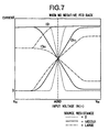
- Figures 6 and 7 are graphs of the change of the internal operating voltage-input voltage dependency of the differential amplifier circuit due to the source resistance value and the change of the current-input voltage dependency due to the source resistance value where there is no above negative feedback.
- Figure 8 shows an example of another configuration of a 2-terminal input differential amplifier circuit.
- the current mirror circuit comprising the pMOS transistors ML 0 and ML 1 configures the output load circuit of the differential amplifier circuit.
- both of the sources of the transistors ML and ML 1 are connected to the supply line of the power supply voltage V DD , the gates are connected to each other, and the connection point thereof is connected to the drain of the transistor ML 0 .
- the drain of the transistor ML 0 is connected to the drain of the transistor MI 0 configuring the differential pair, the connection point thereof forms the non-inverted output terminal DFO(+), the drain of the transistor ML 1 is connected to the drain of the transistor MI 1 configuring the differential pair, and the connection point thereof forms the inverted output terminal DFO(-).
- the other components besides the load circuit are the same as the components of the 2-terminal input differential amplifier circuit shown in Fig. 2. Namely, the resistance element RS is connected between the source of the transistor MI 0 and the node VS 1 , while the resistance element RS 1 is connected between the source of the transistor MI 1 and the node VS 1 .
- the operating current is supplied to the node VS 1 by the current source configured by the transistor MS 1 to the gate of which the bias voltage V BIAS is supplied.
- Figure 9 shows an example of a conventional 2-terminal input differential amplifier circuit for comparison. As illustrated, in this differential amplifier circuit, resistors are not connected to the source side of the transistors MI 0 and MI 1 configuring the differential pair. The sources of the transistors MI 0 and MI 1 are connected to each other, and the operating current is supplied from the current source comprised of the transistor MS 1 to the node VS 1 of the connection point thereof.
- Figure 10 is a graph of the change of the internal operating voltage-input voltage dependency of a differential amplifier circuit due to the source resistance value in the case where the differential amplifier circuit shown in Fig. 8 and Fig. 9 is operated as a processing circuit supplying negative feedback between the input and the output. Further, Fig. 11 is a graph of the change of the operating current-input voltage dependency due to the source resistance value in this case.
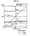
- Figure 12 is a graph of the change of the internal operating voltage-input voltage dependency of the differential amplifier circuit due to the source resistance value in the case where the differential amplifier circuit shown in Fig. 8 and Fig. 9 is operated as a comparison and judgment circuit not supplying negative feedback between the input and the output. Further, Fig. 13 is a graph of the change of the operating current-input voltage dependency due to the source resistance value in this case.
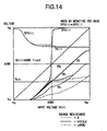
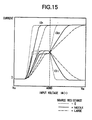
- Figure 14 is a graph of the change of the internal operating voltage-input voltage dependency of the differential amplifier circuit due to the source resistance value in the case where the differential amplifier circuit shown in Fig. 8 and Fig. 9 is operated as a comparison and judgment circuit not supplying negative feedback between the input and the output.
- Fig. 15 is a graph of the change of the operating current-input voltage dependency due to the source resistance value in this case.
- the abscissa indicates an input signal voltage to the non-inverted output terminal DFO(+) of the differential amplifier circuit
- the abscissa indicates the input signal voltage to the inverted output terminal DFO(-) of the differential amplifier circuit.
- the present invention by providing the resistors between the source side of the transistors configuring the differential pair and the current source for supplying the operating current, improvement of the input-output linear characteristic of the differential amplifier circuit and expansion of the dynamic range are achieved.
- the inverted and non-inverted output signals of the differential amplifier circuit mentioned above do not have large output amplitudes since when the processing circuit supplies negative feedback between the input and the output, the amplitude of the output stage divided by the amplification rate of the output stage becomes the output amplitude of the differential amplifier circuit. For this reason, in both of cases of the input-output characteristic of the resistance load type 2-terminal input differential amplifier circuit shown in Fig. 4 and the input-output characteristic of the current mirror circuit load type 2-terminal input differential amplifier circuit shown in Fig. 10, the output signal levels of the non-inverted output terminal DFO(+) and the inverted output terminal DFO(-) become almost equal.
- These output terminals are connected to the drains of the transistors configuring the differential pair and the drain voltage of the transistors are slightly high and substantially constant, therefore both of two input transistors configuring the differential pair operate in the saturation region or one of them operates in the saturation region and the other one is turned off.
- the current flowing through the transistor MI 0 is ID 0i
- the current flowing through the transistor MI 1 is ID 1i
- the summation of the currents ID 0i and ID 1i is ID 1
- ID i becomes equal to ID 01
- ID 1i becomes equal to 0.
- the current ID i is equal to the operating current supplied to the differential pair.
- the 2-terminal input differential amplifier circuit shown in Fig. 2 or Fig. 8 it becomes equal to the current flowing through the transistor MS 1 acting as the current source.
- V si V INi - - V th - ⁇ si / ⁇ i 1 / 2 ⁇ V BIAS - V th
- V si V INi - / + - V th - ⁇ si / 2 ⁇ ⁇ i 1 / 2 ⁇ V BIAS - V th
- V si V INi + - V th - ⁇ si / ⁇ i 1 / 2 ⁇ V BIAS - V th
- V x 2 / ⁇ i 1 / 2 ⁇ ID 1 ⁇ i 1 / 2 - ID oi 1 / 2
- ID 0i and ID 1i change in a range from 0 to ID i and a range from ID i to 0 about ID i /2 as the center. Namely, they change by (ID i )/2) ⁇ (ID i /2).
- V x 2 / ⁇ i 1 / 2 ⁇ ID 1 ⁇ i 1 / 2 - ID oi 1 / 2 + R i ⁇ ID 1 ⁇ i - ID oi
- the current value of ID 0i and ID 1i changes in a range from 0 to ID i and a range from ID i to 0 about ID i /2 as the center. Namely, it changes by (ID i /2) ⁇ (ID i /2).
- the drain of the transistor configuring the current source that is, the voltage V Si of the node VS 1 shown in Fig. 2 and Fig. 6, is lowered from that of the case when resistances are not inserted by an amount of the voltage drop (R i ⁇ ID i ) due to the inserted resistances.
- the differential amplifier circuit of the present invention by inserting resistances between sources of the transistors configuring the differential pair and the drain of the transistor configuring the current source and separating the sources of the transistors configuring the differential pair, when the voltage level of the input signal is higher than the analog ground voltage AGND, that is, when the transistors configuring the differential pair are turned on more, the voltage range in which the level change of the input signal and the change of the output current have a linear relationship is expanded by exactly an amount of (R i ⁇ ID i ) according to the resistance value R 1 of the source resistor and the supply current ID i of the transistor acting as the current source.
- any of the amplitudes given by above equation (38), equation (44), and equation (51) spreads to the small portion as the amplitude.
- the resistance values of the resistances inserted at the source side of the transistors configuring the differential pair are set large, sometimes the input voltage range in which the linear input characteristic is obtained is only the power supply voltage V DD side from the analog ground voltage AGND or the common voltage VSS side from the analog ground voltage AGND, therefore, it is necessary to appropriately set the resistance values of the resistances inserted at the source side.
- the multi-input differential amplifier circuit has a more complex circuit configuration than the usual 2-terminal input differential amplifier circuit, therefore the capacity component of the load driven by the output of the differential input circuit becomes large.
- a multi-input differential amplifier circuit that can secure a sufficient amplification rate and operating speed is configured by using the differential amplifier circuit as a differential input circuit and providing a push-pull output stage for driving the load circuit and an intermediate differential amplification stage.
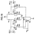
- Figure 16 is a circuit diagram of an example of a 4-input differential amplifier circuit having two differential pairs. Note that, Fig. 17 shows an example of a conventional 4-input differential amplifier circuit for comparison.
- the terminal input differential amplifier circuit of the present example has two differential pairs configured by transistors MI 01 and MI 11 and MI 02 and MI 12 .
- the gates of the transistors MI 01 and MI 11 are connected to the differential input terminals IN 1 (-) and IN 1 (+), and the gates of the transistors MI 02 and MI 12 are connected to the differential input terminals IN 2 (-) and IN 2 (+).
- the sources of the transistors MI 01 and MI 11 are connected to the node VS 1 via the resistance elements RS 01 and RS 11 and the sources of the transistors MI 02 and MI 12 are connected to the node VS 2 via the resistance elements RS 02 and RS 12 .
- the transistor MS 1 to the gate of which the bias voltage V BIAS is supplied is connected between the node VS 1 and the common voltage V ss
- the transistor MS 2 to the gate of which the bias voltage V BIAS is supplied is connected between the node VS 2 and the common voltage V SS .
- the bias voltage V BIAS is set in its voltage level so that the transistors MS 1 and MS 2 operate in the non-saturation region.
- the transistors MS 1 and MS 2 configure the current sources for supplying the operating currents to the differential pairs.
- Both of the drains of the transistors MI 01 and MI 02 are connected to the non-inverted output terminal DFO(+), while both of the drains of the transistors MI 01 and MI 12 are connected to the inverted output terminal DFO(-).
- a resistance element RL 0 configuring the output load is connected between the non-inverted output terminal DFO(+) and the supply line of the power supply voltage V DD
- a resistance element RL 1 configuring the output load is connected between the inverted output terminal DFO(-) and the supply line of the power supply voltage V DD .
- resistance elements are inserted between the sources of the transistors configuring the differential pairs and the current sources for supplying the operating currents. Namely, the sources of the transistors configuring the differential pair are separated by the inserted resistance elements.
- the sources of the transistors configuring the differential pairs are directly connected to the drains of the transistors configuring the current sources not through the resistance elements.
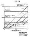
- Figure 18 is a graph of the change of the internal operating voltage-input voltage dependency due to the source resistance value in the case where the 4-terminal input differential amplifier circuit shown in Fig. 16 and Fig. 17 is operated as a processing circuit supplying negative feedback between the input and the output. Further, Fig. 19 is a graph of the change of the operating current-input voltage dependency due to the source resistance value in this case.
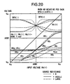
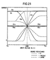
- Figure 20 is a graph of the change of the internal operating voltage-input voltage dependency due to the source resistance value in the case where the 4-terminal input differential amplifier circuit shown in Fig. 16 and Fig. 17 is operated as a comparison and judgment circuit not supplying negative feedback between the input and the output.
- Fig. 21 is a graph of the change of the operating current-input voltage dependency due to the source resistance value in this case.
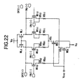
- Figure 22 shows another example of the configuration of a 4-terminal input differential amplifier circuit.
- the load circuit in comparison with the 4-terminal input differential amplifier circuit shown in Fig. 16, the load circuit is configured by a current mirror circuit comprising pMOS transistors ML 0 and ML 1 in place of the resistance elements RL 0 and RL 1 . Except for the load circuit, the rest of the components are substantially the same as those of the 4-terminal input differential amplifier circuit exemplified in Fig. 16.
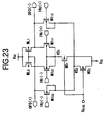
- Fig. 23 shows for comparison an example of a conventional 4-terminal input differential amplifier circuit in which the load circuit is configured by a current mirror circuit.
- resistance elements are inserted between the sources of the transistors configuring the differential pair and the transistor configuring the current source for supplying the operating current to each differential pair. Contrary to this, there are no resistance elements on the source side of the transistors configuring the differential pair in the conventional 4-terminal input differential amplifier circuit - the source of each transistor is directly connected to the transistor configuring the current source.
- Figure 24 is a graph of the change of the internal operating voltage-input voltage dependency due to the source resistance value in the case where the 4-terminal input differential amplifier circuit shown in Fig. 22 and Fig. 23 is operated as a processing circuit supplying negative feedback between the input and the output.
- Fig. 25 is a graph of the change of the operating current-input voltage dependency due to the source resistance value in this case.
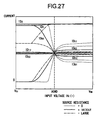
- Figure 26 is a graph of the change of the internal operating voltage-input voltage dependency due to the source resistance value in the case where the 4-terminal input differential amplifier circuit shown in Fig. 22 and Fig. 23 is operated as a comparison and judgment circuit not supplying negative feedback between the input and the output. Further, Fig. 27 is a graph of the change of the operating current-input voltage dependency due to the source resistance value in this case.
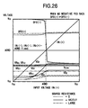
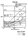
- Figure 28 is a graph of the change of the internal operating voltage-input voltage dependency due to the source resistance value in the case where the 4-terminal input differential amplifier circuit shown in Fig. 22 and Fig. 23 is operated as a comparison and judgment circuit not supplying negative feedback between the input and the output.
- Fig. 29 is a graph of the change of the operating current-input voltage dependency due to the source resistance value in this case. Note that, in Fig. 28 and Fig. 29, the abscissa indicates the input signal voltage on the inverted input terminal IN(-) side.
- the source voltages VR 02 and VR 12 of the transistors MI 02 and MI 12 in the differential pair to which the differential signals are not input, the voltage VS2 of the node VS 2 , and the operating currents ID 02 and ID 12 become substantially constant under the input voltage condition of the case where all of the four input terminals are held at the analog ground voltage AGND.
- the source voltages VR 01 and VR 11 of the transistors MI 01 and MI 11 in the differential pair to which the differential signals are input, the voltage VS 1 of the node VS 1 , and the operating currents ID 0i and ID 1i are substantially the same as those in the operation of the 2-terminal input differential amplifier circuit.
- the operating voltages and the operating currents of the differential pairs configuring the differential amplifier circuit are substantially the same as those of the differential pair configuring a 2-terminal input differential amplifier circuit.
- the linear operation region having the input voltage range of AGND ⁇ 400 mV in the case of no source resistance is enhanced to about AGND+2V to AGND-0.8V by inserting the source resistors.
- differential pairs configured by n-channel MOS transistors were shown as the example, but the present invention is not limited to this.
- the differential pair can be configured also by p-channel transistors.
- bipolar transistors other than MOS transistors are shown as the example, but the present invention is not limited to this.
- the differential pair can be configured also by p-channel transistors.
- bipolar transistors other than MOS transistors are shown as the example, but the present invention is not limited to this.
- the output load circuit of each differential pair is configured by a current mirror circuit or resistor load, but the present invention is not limited to this. It is possible to configure the load circuit by for example pMOS transistors to the gates of which a predetermined bias voltage is supplied or pMOS transistors with both gates and drains connected to the output node.
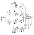
- Figure 30 shows a second embodiment of the multi-input differential amplifier circuit of the present invention.
- the differential amplifier circuit of the present embodiment has substantially the same configuration as that of the first embodiment of the differential amplifier circuit shown in Fig. 1, but the transistors to the gates of which the predetermined bias voltage is supplied are connected to the source side of the transistors configuring each differential pair in place of the resistance elements.
- n-channel MOS transistors MR 01 and MR 11 are connected between the sources of the transistors MI 01 and MI 11 and the node VS 1 .
- n-channel MOS transistors MR 0n and MR 1n are connected between the sources of the transistors MI 0n and MI 1n and the node VS n .
- a bias voltage V G is supplied to the gates of the transistors MR 1 and MR n .
- the bias voltage V G is a voltage that is set so that the transistors MR 01 , MR 11 ,..., MR 0n and MR 1n operate in the non-saturation region and is set at the power supply voltage V DD , the common voltage V SS , or a predetermined voltage between the power supply voltage V DD and the common voltage V SS according to the configuration etc. of the circuit.
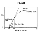
- the abscissa indicates the drain voltage V D of the transistor
- the ordinate indicates the current ID 01 of the transistor.
- the transistor equivalently has a characteristic as a resistance element.
- VR 01 is the source voltage of the transistor MI 0i or MI 1i configuring the differential pair as shown in Fig. 30, while V Si is the source voltage of the transistor MR 0i or MR 1i configuring the source resistor.
- the transistor When the drain voltage V D of the transistor exceeds the voltage VR 01 , the transistor enters the saturation region. In this case, the linear relationship disappears between the current ID 0i flowing through the transistor and the drain voltage V D .
- the gate voltage V G is high like the power supply voltage V DD , as illustrated, the rates of change of the current ID 0i and the drain voltage V D are held at almost constant ratios. For this reason, in the multi-input differential amplifier circuit shown in Fig. 30, by setting the bias voltage V G to be input to the gates of the transistors MR 01 , MR 11 ,..., MR 0n and MR 1n at a high voltage, for example, the power supply voltage V DD , the transistors act as resistance elements.
- the sources of the transistors configuring the differential pairs are connected to the current sources for supplying the operating currents to the differential pairs via the resistance elements or the transistors to the gates of which the predetermined bias voltage is supplied.
- the sources of the transistors configuring the differential pair are separated by the resistance elements or the transistors acting as the resistance elements.
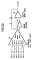
- Figure 32, Fig. 33, and Fig. 34 show examples of the configuration of a multi-input amplifier circuit and multi-input comparison circuit configured using the differential amplifier circuit of the present invention. Note that, in these circuits, the multi-input differential amplifier circuit shown in Fig. 30 mentioned above is used as the multi-terminal differential input circuit (DEF2n).
- Figure 32 shows the example of the configuration of a multi-input amplifier circuit configured by a differential input circuit of 2n-input terminals (DEF2n) 10, a source follower 20, and the push-pull output stage.
- DEF2n 2n-input terminals
- the input terminal of the source follower 20 is connected to the inverted output terminal DFO(-) of the differential input circuit 10.
- the output signal from the inverted output terminal DFO(-) of the differential input circuit 10 and the output signal of the source follower 20 are input to the push-pull output stage 30.
- phase compensation resistance element R 1 and capacitor C 1 are connected in series between the output terminal OUT of the push-pull output stage and the inverted output terminal DFO(-) of the differential input circuit 10.
- Figure 33 shows an example of the configuration of a comparison circuit configured by the 2n-input terminal differential input circuit 10, the source follower 20, and the push-pull output stage 30.
- the circuit configuration of the present example is substantially the same configuration as that of the multi-input amplifier circuit shown in Fig. 32. Note that since the circuit of the present example is used as the comparison circuit, the phase compensation circuit comprising the phase compensation resistance element R 1 and capacitor C 1 connected in series shown in Fig. 32 is omitted.
- Figure 34 shows an example of the configuration of a differential amplifier circuit configured by the 2n-input terminal differential input circuit 10, a 2-terminal input differential amplifier circuit 40, and an inverter output stage 50.
- the inverted output terminal DFO(-) and the non-inverted output terminal DFO(+) of the 2n-terminal differential input circuit 10 are connected to the non-inverted input terminal In(+) and the inverted input terminal In(-) of the 2-terminal input differential amplifier circuit 40.
- the inverted output terminal DFO(-) of the 2-terminal input differential amplifier circuit 40 is connected to the input terminal of the inverter output stage 50.
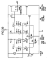
- Figure 35 to Fig. 40 show examples of the concrete configuration of the multi-input amplifier circuit and the multi-input comparison circuit configured using the differential amplifier circuit of the present invention. Note that, in these circuits, a 4-terminal or 6-terminal input differential amplifier circuit is configured by using the multi-input differential amplifier circuit of the first and second embodiments shown in Fig. 1 and Fig. 30.
- Figure 35 shows an example of the multi-input differential amplifier circuit configured by the 4-terminal input differential input circuit 10a, source follower 20, push-pull output stage 30, and a bias circuit 12.
- the bias circuit 12 is configured by a current source IS 0 and an nMOS transistor MS 0 connected in series between the supply line of the power supply voltage V DD and the common voltage V ss .
- the gate and the drain of the transistor MS 0 are commonly connected to the current source IS 0 . while the source is connected to the common voltage V ss .
- the bias voltage V BIAS is output from the connection point of the gate and the drain of the transistor MS 0 .
- the 4-terminal input differential input circuit is configured by two differential pairs configured by nMOS transistors MI 01 , MI 11 , MI 02 , and MI 12 . Further, the pMOS transistors ML 0 and ML 1 configure the current mirror circuit, while that current mirror circuit configures the output load circuit of the differential input circuit.
- the gates of the transistors MI 01 and MI 11 are connected to the differential input terminals IN(+) and IN(-).
- the drains of the transistors Mi 01 and MI 11 are connected to the output terminals DFO(+) and DFO(-), and the sources are connected to the node VS 1 via the resistance elements RS 01 and RS 11 .
- the nMOS transistor MS 1 configures the current source for supplying the operating current to the transistors MI 01 and MI 11 .
- the drain of the transistor MS 1 is connected to the node VS 1 , the source is connected to the common voltage V ss , and the bias voltage V BIAS generated by the bias circuit 12 is input to the gate.
- the sources of the transistors MI 02 and MI 12 are connected to the VS 2 via the resistance elements RS 02 and RS 12 , and the operating current is supplied to the node VS 2 by the transistor MS 2 to the gate of which the bias voltage V BIAS is supplied.
- the source follower 20 is configured by the nMOS transistors ML 2 and MS 3 .
- the transistors ML 2 and MS 3 are connected in series between the supply line of the power supply voltage V DD and the common voltage V ss .
- the gate of the transistor ML 2 is connected to the inverted output terminal DFO(-) of the 4-terminal input differential input circuit 10a, while the source is connected to the gate of the transistor NT 1 configuring the push-pull output stage 30.
- the gate of the transistor MS 3 is supplied with the bias voltage V BIAS . Namely, the transistor MS 3 configures the current source for supplying the operating current to the emitter of the transistor ML 2 .
- a pMOS transistor PT 1 and an nMOS transistor NT 1 are connected in series between the supply line of the power supply voltage V DD and the common voltage V ss .
- the gate of the transistor PT 1 is connected to the inverted output terminal DFO(-) of the 4-terminal input differential input circuit 10a, while the gate of the transistor NT 1 is connected to the source of the transistor ML 2 configuring the source follower 20.
- the output terminal OUT is formed by the connection point of the transistors PT 1 and NT 1 .
- the resistance element R 1 and the capacitor C 1 are connected in series between the output terminal OUT and the inverted output terminal DFO(-) of the 4-terminal input differential input circuit 10a.
- the phase compensation circuit is configured by the resistance element R 1 and the capacitor C 1 . The phase compensation circuit prevents the oscillation of the circuit when negative feedback is applied.
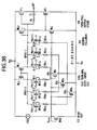
- Figure 36 shows an example of a multi-input differential amplifier circuit configured by a 6-terminal input differential input circuit 10b, source follower 20, push-pull output stage 30, and bias circuit 12.
- the bias circuit 12 the source follower 20, and the push-pull output stage 30 have the same configurations as those of the partial circuits of the example of the circuit shown in Fig. 35.
- an explanation will be made of the configuration of the multi-input differential input circuit of the present example centered on the 6-terminal input differential input circuit 10b.
- the 6-terminal input differential input circuit 10b three differential pairs are configured by the transistors MI 01 , MI 02 , and MI 03 and MI 01 , MI 12 , and MI 13 .
- the gates of the transistors MI 01 , MI 12 , and MI 13 configure positive side input terminals, while the gates of the transistors MI 01 , MI 02 , and MI 03 configure negative side input terminals.
- the drains of the positive side transistors are connected to the inverted output terminal DFO(-), while the drains of the negative side transistors are connected to the non-inverted output terminal DFO(+).
- the pMOS transistor ML 0 is connected between the supply line of the power supply voltage V DD and the non-inverted output terminal DFO(+), while the pMOS transistor ML 1 is connected between the supply line of the power supply voltage V DD and the inverted output terminal DFO(-).
- the gates of the transistors ML 0 and ML 1 are connected to each other, and the connection point thereof is connected to the drain of the transistor ML 0 .
- the current mirror circuit is configured by these transistors. That current mirror circuit configures the load circuit of the 6-terminal input differential input circuit.
- the ratio of the current amplification rates of the transistors MS 1 , MS 2 , and MS 3 acting as the current sources for supplying the operating currents to the differential pairs is set at A:B:C in the same way as the transistors configuring the differential pair.
- the resistance value of the resistance elements RS 01 , and RS 11 connected between the sources of the transistors configuring each differential pair and the current source is R A
- the resistance value of the resistance elements RS 02 and RS 12 is R B
- the resistance value of the resistance elements RS 03 and RS 13 is R c
- R A :R B :R C (1/A):(1/B):(1/C) is set.
- the sources of the transistors MI 01 and MI 11 are connected via the resistance elements RS 01 and RS 11 to the node VS 1 .
- the transistor MS 1 is connected between the node VS 1 and the common voltage V ss .
- the sources of the transistors MI 02 and MI 12 are connected via the resistance elements RS 02 and RS 12 to the node VS 2 .
- the transistor MS 2 is connected between the node VS 2 and the common voltage V ss .
- the sources of the transistors MI 03 and MI 13 are connected via the resistance elements RS 03 and RS 13 to the node vs3.
- the transistor MS 3 is connected between the node vs3 and the common voltage V ss .
- the bias voltage V BIAS generated by the bias circuit 12 is supplied to the gates of the transistors MS 1 , MS 2 , and MS 3 .
- the current sources for supplying the operating currents to the differential pairs are configured by the transistors MS 1 , MS 2 , and MS 3 .
- the differential input signals input to the differential input terminals IN 1 (+) and IN 1 (-), IN 2 (+) and IN 2 (-), and IN 3 (+) and IN 3 (-) are weighted with the ratio of A:B:C, and the amplified signals are output from the output terminal OUT of the push-pull output stage.
- Figure 37 shows the example of another circuit of the multi-input differential amplifier circuit configured by a 4-terminal input differential input circuit 10c, the source follower 20, push-pull output stage 30, and the bias circuit 12. Except for the 4-terminal input differential input circuit 10c, the rest of the components have the same configuration as those of the partial circuits of the example of the circuit shown in Fig. 35. Below, an explanation will be made of the configuration of the multi-input differential amplifier circuit of the present example focusing on the 4-terminal input differential input circuit 10c.
- the 4-terminal input differential input circuit 10c in the multi-input differential amplifier circuit of the present example has two differential pairs configured by the transistors MI 01 , MI 11 and MI 02 , MI 12 , the load circuit configured by the resistance elements RL 0 and RL 1 , and the current sources configured by the transistors MS 1 and MS 2 .
- the output load circuit is configured by the resistance elements RL 0 and RL 1 in place of the current mirror circuit comprising the transistors ML 0 and ML 1 .
- the current amplification rate of the transistors MI 01 and MI 11 configuring the two differential pairs in the circuit of the present example is ⁇ 1
- the current amplification rates of the transistors MI 02 and MI 12 is ⁇ 2
- ⁇ 1 : ⁇ 2 A:B
- the ratio of the current amplification rates of the transistors MS 1 and MS 2 acting as the current sources for supplying the operating currents to the differential pairs is set at A:B in the same way as the transistors configuring the differential pair.
- R A the resistance value of the resistance elements RS 01 and RS 11 connected between the sources of the transistors configuring each differential pair and the current source
- R B the resistance value of the resistance elements RS 02 and RS 12
- the differential input signals input to the differential input terminals IN(+) and IN(-) and IN 2 (+) and IN 2 (-) are weighted with the ratio of A:B, and the amplified signals are output from the output terminal OUT of the push-pull output stage.
- Figure 38 shows another example of the circuit of the multi-input differential amplifier circuit configured by a 4-terminal input differential input circuit 10d, the source follower 20, push-pull output stage 30, and the bias circuit 12. Except for the 4-terminal input differential input circuit 10d, the rests of the components have the same configuration as those of the partial circuits of the example of the circuit shown in Fig. 35. Below, an explanation will be made of the configuration of the multi-input differential amplifier circuit of the present example focusing on the 4-terminal input differential input circuit 10d.
- the 4-terminal input differential input circuit 10d is configured by two differential pairs configured by the transistors MI 01 , MI 11 and MI 02 , MI 12 , the current mirror circuit comprising the transistors ML 0 and ML 1 configuring the output load of these differential pairs, the transistors MR 01 , MR 11 , MR 02 , and MR 12 which are connected to the source side of the transistors MI 01 , MI 11 and MI 02 , MI 12 configuring the differential pairs and act as the resistance elements, and the transistors MS 1 and MS 2 for supplying the operating currents to the differential pairs.
- nMOS transistors MR 01 , MR 11 , MR 02 , and MR 12 are provided in place of the resistance elements.
- the transistor MR 01 is connected between the transistor MI 01 and the node VS 1
- the transistor MR 11 is connected between the transistor MI 01 and the node VS 1
- the transistor MR 02 is connected between the transistor MI 02 and the node VS 2
- the transistor MR 12 is connected between the transistor MI 12 and the node VS 2 .
- the power supply voltage V DD is supplied to the gates of the transistors MR 01 , MR 11 , MR 02 , and MR 12 , so these transistors operate in the non-saturation region.
- the ratio of the current amplification rates of the transistors MS 1 and MS 2 acting as the current sources for supplying the operating currents to the differential pairs is set at A:B in the same way as the transistors configuring the differential pair.
- R A an equivalent resistance of the transistors MR 01 and MR 11 which are connected between the source of the transistors configuring each differential pair and the transistor configuring the current source and provided as the resistance elements
- R B the equivalent resistance of the transistors MR 02 and MR 12
- the differential input signals input to the differential input terminals IN(+) and IN(-) and IN 2 (+) and IN 2 (-) are weighted with the ratio of A:B, and the amplified signals are output from the output terminal OUT of the push-pull output stage.
- Figure 39 shows an example of another circuit of the multi-input differential amplifier circuit configured by a 4-terminal input differential input circuit 10e, the source follower 20, push-pull output stage 30, and the bias circuit 12. Except for the 4-terminal input differential input circuit 10e, the rest of the components have the same configuration as those of the partial circuits of the example of the circuit shown in Fig. 38. Below, an explanation will be made of the configuration of the multi-input differential amplifier circuit of the present example focusing on the 4-terminal input differential input circuit 10e.
- the 4-terminal input differential input circuit 10e is configured by two differential pairs configured by the transistors MI 01 , MI 11 and MI 02 , MI 12 , resistance elements RL 0 and RL 1 configuring the output loads of these differential pairs, the transistors MR 01 , MR 11 , MR 02 , and MR 12 which are connected to the source side of the transistors MI 01 , MI 11 and MI 02 , MI 12 configuring the differential pairs and equivalently act as the resistance elements, and the transistors MS 1 and MS 2 for supplying the operating currents to the differential pairs.
- the resistance elements RL 0 and RL 1 are used for the output load circuit in place of the current mirror circuit comprising the transistor.
- the rest of the circuit configuration is substantially the same as that of the example of the circuit shown in Fig. 38.
- the differential input signals input to the differential input terminals IN(+) and IN(-) and IN 2 (+) and IN 2 (-) are weighted with the ratio of A:B, and the amplified signals are output from the output terminal OUT of the push-pull output stage.
- Figure 40 shows an example of the multi-input differential amplifier circuit configured by the 4-terminal input differential input circuit 10a, differential amplifier circuit 40, inverter output stage 50, and the bias circuit 12.
- the 4-terminal input differential input circuit 10a has the same configuration as that of the 4-terminal input differential input circuit 10a in the example of the circuit shown in Fig. 35, therefore, here, this partial circuit is indicated by assigning the same reference numeral 10a as that of Fig. 35.
- the differential amplifier circuit 40 is configured by the differential pair comprising the nMOS transistors NT 2 and NT 3 , the current mirror circuit comprising the pMOS transistors PT 2 and PT 3 , and the current source configured by the nMOS transistor MS 3 .
- the gate of the transistor NT 2 configuring the differential pair is connected to the non-inverted output terminal DFO(+) of the 4-terminal input differential input circuit 10a, while the gate of the transistor NT 3 is connected to the inverted output terminal DFO(-).
- the sources of the transistors NT 2 and NT 3 are connected to the node vs3.
- the sources of the transistors PT 2 and PT 3 are connected to the supply line of the power supply voltage V DD , the gates of these transistors are commonly connected, and the connection point thereof is connected to the drain of the transistor PT 2 .
- the drains of the transistors PT 2 and PT 3 are connected to the drains of the transistors NT 2 and NT 3 . Namely, the current mirror circuit comprising the transistors PT 2 and PT 3 configures the load circuit of the differential amplifier circuit 40.
- the drain of the transistor MS 3 is connected to the node vs3, and the source is connected to the common voltage V ss .
- the bias voltage V BIAS generated by the bias circuit 12 is supplied to the gate of the transistor MS 3 .
- the transistor MS 3 forms the current source for supplying the operating current to the differential pair configured by the transistors NT 2 and NT 3 .
- the inverter output stage 50 is configured by the pMOS transistor PT 1 and the nMOS transistor NT 1 .
- the transistors PT 1 and NT 1 are connected in series between the supply line of the power supply voltage V DD and the common voltage V ss , the gates of these transistors are connected to each other, and the connection point thereof is connected to the output terminal of the differential amplifier circuit 40, that is, the connection point of the drains of the transistor PT 3 and the transistor NT 3 .
- the connection point of the drains of the transistor PT 1 and the transistor NT 1 forms an output terminal OUTZ of the inverter output stage 50.
- the differential input signals input to the differential input terminals IN(+) and IN(-), IN 2 (+) and IN 2 (-) are amplified at the 4-terminal input differential input circuit 10a, and the amplified differential signals are output to the non-inverted output terminal DFO(+) and the inverted output terminal DFO(-) of the 4-terminal input differential input circuit 10a.
- the output differential signals of the 4-terminal input differential input circuit 10a are further amplified by the differential amplifier circuit 40, and the obtained amplified signals are inverted via the inverter output stage 50 and output from the output terminal OUTZ of the inverter output stage 50 as single end signals.
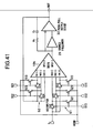
- Figure 41 shows an embodiment of the multi-input differential amplifier circuit configured by a switch circuit 60 for switching the input to the input terminals of the differential input circuit, 6-terminal input differential input circuit 10b, source follower 20, and the push-pull output stage 30.
- the switch circuit 60 is configured by a positive side switch circuit 61 and a negative side switch circuit 62.
- the positive side switch circuit 61 is configured by switches S11, S12, S21, S22, S31, and S32.
- the switches S11 and S12 are controlled by a control signal SI1
- the switches S21 and S22 are controlled by a control signal SI2
- the switches S31 and S32 are controlled by a control signal SI3.
- the negative side switch circuit 62 is configured by switches S13, S14, S23, and S24.
- the switches S13 and S14 are controlled by a control signal SO1
- the switches S23 and S24 are controlled by a control signal SO2.
- the positive side input terminals IN 1 (+), IN 2 (+), and IN3(+) of the 6-terminal input differential input circuit 10b are connected to a signal input terminal T S when the control signals SI1, SI2, and SI3 are at a high level, while are connected to the analog ground voltage AGND when the control signals SI1, SI2, and SI3 are at a low level.
- the negative side input terminals IN 1 (-), IN 2 (-), and IN S (-) are connected to the output terminal OUT when the control signals SO1 and SI2 are at high level and are connected to the analog ground voltage AGND when the control signals SO1 and SI2 are at a low level.
- the negative side input terminal IN3(-) is connected to the output terminal OUT of the push-pull output stage 30, therefore the negative feedback is always applied.
- the 6-terminal input differential input circuit 10b has the same configuration as that of for example the 6-terminal input differential input circuit 10b shown in Fig. 26 in the fourth embodiment mentioned above. Here, it is indicated by assigning the same reference numeral 10b as that of Fig. 36 to this partial circuit.
- the 6-terminal input differential input circuit 10b is set so that conductances of the transistors configuring the differential input elements, the resistance elements connected to the source side of the transistors, and the transistor acting as the current source for supplying the operating current to the differential pair are different for every differential pair. For this reason, the differential input signals input to the differential input terminals IN 1 (+) and IN 1 (-), IN 2 (+) and IN 2 (-), and IN 3 (+) and IN S (-) are weighted and amplified.
- the differential input signals input to the differential input terminals IN 1 (+) and IN 1 (-), IN 2 (+) and IN 2 (-), and IN 3 (+) and IN 3 (-) are weighted with the ratio of 1:2:3.
- V IN1 (+), V IN2 (+), and V IN3 (+) are input signal voltages to the positive side input terminals IN 1 (+), IN 2 (+), and IN 3 (+), and V IN1 (-), V IN2 (-), and V IN3 (-) are input signal voltages to the negative side input terminals IN 1 (-), IN 2 (-), and IN 3 (-).
- V IN ⁇ 3 - v out
- G is the gain of the multi-input differential amplifier circuit of the present embodiment.
- any integer from 0 to 6 can be set by the signals SI 1 , SI 2 , and SI 3
- any integer from 3 to 6 can be set by the signals SO 1 and SO 2 .
- Figure 42 is a circuit diagram of an embodiment of the operational amplifier circuit of a gain of 1/2 configured by using the 4-terminal input differential amplifier circuit.
- the operational amplifier circuit of the present embodiment is configured by a 4-terminal input differential amplifier circuit 100. Both of the inverted input terminals IN 1 (-) and IN 2 (-) of the 4-terminal input differential amplifier circuit 100 are connected to the output terminal OUT.
- the non-inverted input terminal IN 1 (+) is connected to the input terminal T S of the input signal v in , and the non-inverted input terminal IN 2 (+) is connected to the analog ground voltage AGND.
- the 4-terminal input differential amplifier circuit 100 of the present embodiment has the same configuration as that of the 4-terminal input differential amplifier circuit 10 shown in Fig. 35 or Fig. 38.
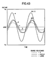
- Figure 43 shows a waveform at the operation of the differential amplifier circuit of the present embodiment.
- a indicates the input signal v in
- b indicates the output signal when there is no source resistor
- c indicates the output signal when the source resistance is a medium extent
- d indicates the waveform of the output signal V out when the source resistance is large.
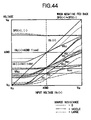
- Figure 44 is a graph of the change of the internal operating voltage-input voltage dependency due to the source resistance value of the differential input circuit part of the operation amplifier circuit of a 1/2 gain using the multi-input differential amplifier circuit of the present embodiment.
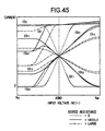
- Fig. 45 is a graph of the change of the operating current-input voltage dependency due to the source resistance value of the differential input circuit part.
- Figure 46 shows an embodiment of a 4-terminal input comparison circuit (COMP4) configured by a 4-terminal input differential amplifier circuit 100a.
- the 4-terminal input differential amplifier circuit 100a configuring the comparison circuit of the present embodiment one the same as the 4-terminal input differential amplifier circuit 100 configuring the operation amplifier circuit shown in Fig. 42 can be used. Note that since the present embodiment configures a comparison circuit, the phase correction circuit in the differential amplifier circuit can be omitted.
- the inverted input terminals IN 1 (-) and IN 2 (-) of the 4-terminal input differential amplifier circuit 100a are connected to the input terminals of the reference voltages V REF1 and V REF2 .
- Both of the non-inverted input terminals IN 1 (+) and IN 2 (+) are connected to the input terminal of the input signal v in .
- Figure 47 indicates the relationship of a timing of the level change of the input signal and the output signal and the value of the resistances connected to the source side of the transistors configuring the differential pair.
- a indicates the input signal v in
- b indicates the output signal where there is no source resistor
- c indicates the output signal in the case where the source resistance is of an intermediate extent
- d indicates the waveform of the output signal v out when the source resistance is large.
- the comparison circuit is configured by a multi-input differential amplifier circuit in which resistances are connected to the source side of the transistors configuring the differential pair, the characteristic is enhanced and the delay time inherent in the comparison circuit can be shortened.
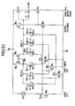
- Figure 48 shows an embodiment of the comparison and judgment circuit configured by the 4-terminal input differential amplifier circuit 100 and a switch circuit 70 for switching the input to the differential amplifier circuit 100.
- the switch circuit 70 is configured by switches S11, S12, S21, and S22. These switches are controlled by a control signal RST. For example, when the control signal RST is at a high level, the inverted input terminals IN 1 (-) and IN 2 (-) of the 4-terminal input differential amplifier circuit 100 are connected to the input terminal of a reset voltage V RST , while when the control signal RST is at low level, the inverted input terminals IN 1 (-) and IN 2 (-) are connected to the output terminal having for example an upper limit value V TOP and a lower limit value V BOT of a peak detection circuit.
- the comparison and judgment circuit configured by the 4-terminal input differential amplifier circuit as in the present embodiment, for example, when the control signal RST is at a high level, the level of the input signal v in and V RST /2 are compared and the level of the output signal V out is set according to the result thereof. On the other hand, when the control signal RST is at a low level, the level of the input signal v in and the level of (V TOP +V BOT )/2 are compared, and the level of the output signal v out is set according to the result of the comparison.
- the linear input-output characteristic can be obtained with respect to a sufficiently wide input voltage range in the differential amplifier circuit 100.
- the characteristic of the comparison and judgment circuit can be enhanced.
- the voltage range in which a linear characteristic can be obtained between the input and the output can be broadened and the dynamic range can be extended. For this reason, there is the advantage that the performances of the processing circuit and the comparison and judgment circuit configured by the differential amplifier circuit can be enhanced.
Description
- The present invention relates to a multi-input differential amplifier circuit having two or more pairs of positive and negative input terminals.
- In a differential amplifier circuit, particularly a multi-input type differential amplifier circuit having two or more pairs of positive and negative input terminals, use is made of a configuration in which an input dynamic range is broadened by connecting drains of transistors configuring a positive side input element to a common node, connecting drains of transistors configuring a negative side input element to another common node, and supplying an operating current by a different current source for every differential pair. A multi-input type differential amplifier circuit having such a configuration was disclosed in Japanese Unexamined Patent Publication (Kokai)
No. 9-93052 - Figure 49 is a circuit diagram of an example of the multi-input type differential amplifier circuit disclosed in Japanese Unexamined Patent Publication (Kokai)
No. 9-93052 - Figure 50 is a view of an example of the multi-input type differential amplifier circuit shown in Fig. 49. Note that, here, a so-called 4-terminal input differential amplifier circuit having two positive and negative input terminals is shown.
- As illustrated, in this differential amplifier circuit, an output load circuit is configured by a current mirror circuit configured by p-channel MOS transistors ML0 and ML1. Namely, both of the sources of the transistors ML0 and ML1 are connected to the supply line of the power supply voltage VDD, the gates of these transistors are connected to each other, and a connection point thereof is connected to the drain of the transistor ML0. The drain of the transistor ML0 is connected to the common node NDp of the drains of the positive side transistors MI01 and MI02, while the drain of the transistor ML1 is connected to the common node NDN of the negative side transistors MI11 and MI12.
- Further, the current source for supplying the operating current to each differential pair is configured by n-channel MOS transistors MS1 and MS2 to the gate of which a predetermined bias voltage is applied. For example, the drain of the transistor MS1 is connected to the node VS1, while the drain of the transistor MS2 is connected to the node VS2. A bias voltage VBIAS is input to the gates of these transistors MS1 and MS2. Note that the bias voltage VBIAS is created by the current source IS0 and the nMOS transistor MS0.
- The node NDP and the node NDN configure a non-inverted output terminal DFO(+) and an inverted output terminal DFO(-) of the differential amplifier circuit. The output signal of the inverted output terminal DFO(-) is input to a push-pull output stage configured by transistors PT1 and NT1 via a source follower configured by transistors ML2 and MS3. The output signal of the source follower is amplified by the push-pull output stage and output to the output terminal OUT. Note that a resistance element R1 and a capacitor C1 forming a phase compensation circuit are connected in series between the inverted output terminal DFO(-) of the differential amplifier circuit and the output terminal OUT of the push-pull output stage.
- Figure 51 is a view of an example of another configuration of the multi-input type differential amplifier circuit. As illustrated, the differential amplifier circuit of the present example is a 6-terminal input differential amplifier circuit configured by three differential pairs. The configuration of the circuit of the example is substantially the same as the 4-terminal input differential amplifier circuit shown in Fig. 50 except that it has three differential pairs. Note that in this circuit, the current amplification rates of the transistors configuring the differential pairs are set to different values, therefore an amplification signal weighted with respect to the input signal is obtained.
- When the current amplification rate of transistors MI01 and MI11 is β1, the current amplification rate of the transistors MI02 and MI12 is β2, the current amplification rate of transistors MI03 and MI13 is β3, and the ratio of the current amplification rates of the transistors MS1, MS2, and MS3 is β1:β2:β3, the differential signal input to each differential pair is weighted in accordance with the current amplification rate of the transistors configuring each differential pair, thus the amplification signal is obtained.
- In the multi-input type differential amplifier circuit mentioned above, when the differential amplifier circuit is used by supplying a negative feedback between the input and the output, the usual differential amplifier circuit having only one pair of positive and negative input terminals operates based on a state where the voltage of the positive side input terminal and the voltage of the negative side input terminal are equal (virtual ground), but in contrast, in a multi-input type differential amplifier circuit, the voltage of the positive side input terminal and the voltage of the negative side input terminal do not have to be equal for every pair, so it operates based on a state where the summation of voltages of the positive side input terminals and the summation of voltages of the negative side input terminals become equal.
- Namely, a multi-input type differential amplifier circuit must operate even in a case where voltages of the positive side input terminal and the negative side input terminal are different for every differential pair. When looking at the drain voltage of the transistor configuring a current source for supplying an operating current to a differential input pair, however, this becomes the output voltage of an OR type source follower circuit using positive and negative input terminals as two input terminals. For this reason, when there is a difference between the voltages of the positive and negative input terminals of more than the threshold voltage of the transistors configuring an input element, the output voltage of the OR type source follower circuit becomes a voltage shifted from the gate voltage of the transistor which is further turned on between the two transistors configuring the input element by the value of the threshold voltage Vth, so a voltage required for turning on the related transistor will not be supplied between the gate and the source of the transistor configuring the other input element.
- As a result, when the voltages of the positive and negative input terminals are separated from each other more than the value of the threshold voltage Vth of the transistors configuring the input element, a state where a current regulated by a constant current source flows through the transistors configuring one input element, while no current flows through the transistors configuring the other input element is exhibited, so there is the disadvantage that it no longer appears as a change of the current. This means that the voltage change of the node to which the drains of the transistors configuring the positive side input element, that is, the output of the differential input circuit, are commonly connected and the other node to which the drains of the transistors configuring the negative side input element are commonly connected, that is, the inverted output terminal and the non-inverted output terminal of the differential input circuit, deviates from the output voltage expected from a multi-input differential amplifier circuit.
- Note that, in the multi-input type differential amplifier circuit mentioned above, in the case of an operational amplifier circuit configured by supplying negative feedback between the input and the output, the voltage difference between the positive and negative output nodes of the differential input circuit is small, and each voltage becomes substantially constant.
- On the other hand, in the case of a comparison and judgment circuit using a multi-input differential amplifier circuit without supplying a negative feedback, at least one of the positive and negative output nodes of the differential input circuit has amplitude, therefore the voltage conditions under which transistors configuring all input elements and constant current sources have a linear characteristic become further narrower. For this reason, there is the disadvantage that, in the case of the comparison and judgment circuit, the expected characteristics cannot be obtained by just an above multi-input type differential amplifier circuit supplying operating currents by different current sources for every differential input.
- Document Patent Abstract of Japan Vol. 16, No.
JP-A-03 258 109 - An object is to provide a multi-input type differential amplifier circuit capable of maintaining the linear characteristic of the input voltage and the output voltage even in a case where there is a difference between the input voltages of the differential input terminals of more than the threshold voltage of the transistors configuring the differential pair and capable of enhancing the dynamic range and the linear characteristic.
- To achieve the above object, a multi-input type differential amplifier circuit of the present invention is a multi-input differential amplifier circuit having at least two pairs of positive and negative input terminals, comprising at least two differential pairs each comprising a first and a second transistor with control gates which are respectively connected to said positive and negative input terminals, with drains which are respectively connected to first and second output terminals, and with sources which are respectively connected to current supply nodes via first and second resistors, and at least two current sources for supplying operating currents to said current supply nodes in said differential pairs, first and second load circuits being connected between said first and second output terminals and a supply line of a first power supply voltage and configured by resistors connected between said first and second output terminals and the supply line of said first power supply voltage
- Further, a multi-input type differential amplifier circuit of the present invention has at least two differential pairs each comprising a first and a second transistor with control gates which are respectively connected to said positive and negative input terminals, with terminals which are connected to first and second output terminals, and with other terminals which are connected to current supply nodes via third and fourth resistors, and at least two current sources for supplying operating currents to said current supply nodes in said differential pairs, first and second load circuits being connected between said first and second output terminals and a supply line of a first power supply voltage, a predetermined bias voltage being applied to the control gates of said third and fourth transistors.
- Further, in the present invention, preferably said current sources for supplying the operating currents to said each differential pair are each configured by a transistor to the control gate of which the predetermined bias voltage is applied, with one terminal which is connected to said current supply node, and with another terminal which is connected to the supply line of a second power supply voltage.
- Further, in the present invention, said first and second load circuits are configured by first and second load configuring transistors which are connected between said first and second output terminals and the supply line of said first power supply voltage and configure a current mirror circuit.
- These and other objects and features of the present invention will become clearer from the following description of the preferred embodiments given with reference to the accompanying drawings, in which:
- Fig. 1 is a circuit diagram of a first embodiment of a multi-input type differential amplifier circuit according to the present invention:
- Fig. 2 is a circuit diagram of an example of the configuration of a 2-input differential amplifier circuit:
- Fig. 3 is a circuit diagram of an example of a conventional 2-input differential amplifier circuit:
- Fig. 4 is a graph of the change of the internal operating voltage-input voltage dependency due to the source resistance of a processing circuit supplying negative feedback between the input and the output of a 2-input differential amplifier circuit:
- Fig. 5 is a graph of the change of the current-input voltage dependency due to the source resistance of a processing circuit supplying negative feedback between the input and the output of the 2-input differential amplifier circuit:
- Fig. 6 is a graph of the change of the internal voltage-input voltage dependency due to the source resistance of a comparison and judgment circuit in which there is no negative feedback between the input and the output of the 2-input differential amplifier circuit:
- Fig. 7 is a graph of the change of the current-input voltage dependency due to the source resistance of a comparison and judgment circuit in which there is no negative feedback between the input and the output of the 2-input differential amplifier circuit:
- Fig. 8 is a circuit diagram of another example of the configuration of the 2-input differential amplifier circuit:
- Fig. 9 is a circuit diagram of another example of the configuration of a conventional 2-input differential amplifier circuit:
- Fig. 10 is a graph of the change of the internal voltage-input voltage dependency due to the source resistance of a processing circuit supplying negative feedback between the input and the output of a 2-input differential amplifier circuit:
- Fig. 11 is a graph of the change of the current-input voltage dependency due to the source resistance of a processing circuit supplying negative feedback between the input and the output of a 2-input differential amplifier circuit:
- Fig. 12 is a graph of the change of the internal voltage-input voltage dependency due to the source resistance of a comparison and judgment circuit in which there is no negative feedback between the input and the output of the 2-input differential amplifier circuit:
- Fig. 13 is a graph of the change of the current-input voltage dependency due to the source resistance of a comparison and judgment circuit in which there is no negative feedback between the input and the output of a 2-input differential amplifier circuit:
- Fig. 14 is a graph of the change of the internal voltage-input voltage dependency due to the source resistance of a comparison and judgment circuit in which there is no negative feedback between the input and the output of a 2-input differential amplifier circuit:
- Fig. 15 is a graph of the change of the current-input voltage dependency due to the source resistance of a comparison and judgment circuit in which there is no negative feedback between the input and the output of a 2-input differential amplifier circuit:
- Fig. 16 is a circuit diagram of an example of the configuration of a 4-input differential amplifier circuit:
- Fig. 17 is a circuit diagram of an example of a conventional 4-input differential amplifier circuit:
- Fig. 18 is a graph of the change of the internal voltage-input voltage dependency due to the source resistance of a processing circuit supplying negative feedback between the input and the output of a 4-input differential amplifier circuit:
- Fig. 19 is a graph of the change of the current-input voltage dependency due to the source resistance of a processing circuit supplying negative feedback between the input and the output of a 4-input differential amplifier circuit:
- Fig. 20 is a graph of the change of the internal voltage-input voltage dependency due to the source resistance of a comparison and judgment circuit in which there is no negative feedback between the input and the output of a 4-input differential amplifier circuit:
- Fig. 21 is a graph of the change of the current-input voltage dependency due to the source resistance of a comparison and judgment circuit in which there is no negative feedback between the input and the output of a 4-input differential amplifier circuit:
- Fig. 22 is a circuit diagram of another example of the configuration of a 4-input differential amplifier circuit:
- Fig. 23 is a circuit diagram of the example of another configuration of a conventional 4-input differential amplifier circuit:
- Fig. 24 is a graph of the change of the internal voltage-input voltage dependency due to the source resistance of the processing circuit supplying negative feedback between the input and the output of a 4-input differential amplifier circuit:
- Fig. 25 is a graph of the change of the current-input voltage dependency due to the source resistance of a processing circuit supplying negative feedback between the input and the output of a 4-input differential amplifier circuit:
- Fig. 26 is a graph of the change of the internal voltage-input voltage dependency due to the source resistance of a comparison and judgment circuit in which there is no negative feedback between the input and the output of a 4-input differential amplifier circuit:
- Fig. 27 is a graph of the change of the current-input voltage dependency due to the source resistance of a comparison and judgment circuit in which there is no negative feedback between the input and the output of a 4-input differential amplifier circuit:
- Fig. 28 is a graph of the change of the internal voltage-input voltage dependency due to the source resistance of a comparison and judgment circuit in which there is no negative feedback between the input and the output of a 4-input differential amplifier circuit:
- Fig. 29 is a graph of the change of the current-input voltage dependency due to the source resistance of a comparison and judgment circuit in which there is no negative feedback between the input and the output of a 4-input differential amplifier circuit:
- Fig. 30 is a circuit diagram of a second embodiment of a multi-input differential amplifier circuit:
- Fig. 31 is a graph of the operational characteristic of transistors acting as the resistors in the second embodiment of the differential amplifier circuit according to the present invention:
- Fig. 32 is a circuit diagram of an example of the configuration of a third embodiment of the differential amplifier circuit according to the present invention:
- Fig. 33 is a circuit diagram of another example of the configuration of the third embodiment of the differential amplifier circuit according to the present invention:
- Fig. 34 is a circuit diagram of another example of the configuration of the third embodiment of the differential amplifier circuit according to the present invention:
- Fig. 35 is a circuit diagram of an example of the configuration of a fourth embodiment of the differential amplifier circuit according to the present invention:
- Fig. 36 is a circuit diagram of another example of the configuration of the fourth embodiment of the differential amplifier circuit according to the present invention:
- Fig. 37 is a circuit diagram of another example of the configuration of the fourth embodiment of the differential amplifier circuit according to the present invention:
- Fig. 38 is a circuit diagram of another example of the configuration of the fourth embodiment of the differential amplifier circuit according to the present invention:
- Fig. 39 is a circuit diagram of another example of the configuration of the fourth embodiment of the differential amplifier circuit according to the present invention:
- Fig. 40 is a circuit diagram of another example of the configuration of the fourth embodiment of the differential amplifier circuit according to the present invention:
- Fig. 41 is a circuit diagram of an example of the configuration of a fifth embodiment of the differential amplifier circuit according to the present invention:
- Fig. 42 is a circuit diagram of an example of the configuration of a sixth embodiment of the differential amplifier circuit according to the present invention:
- Fig. 43 is a waveform diagram of the operation of the differential amplifier circuit of the sixth embodiment:
- Fig. 44 is a graph of the internal voltage-input voltage dependency due to the source resistance of a differential input circuit part of the operational amplifier circuit of a 1/2 gain using the differential amplifier circuit of the sixth embodiment:
- Fig. 45 is a graph of the current-input voltage dependency due to the source resistance of a differential input circuit part of the operational amplifier circuit of a 1/2 gain using the differential amplifier circuit of the sixth embodiment:
- Fig. 46 is a circuit diagram of the configuration of a comparison circuit of a seventh embodiment of the differential amplifier circuit according to the present invention:
- Fig. 47 is a waveform diagram of the operation of the differential amplifier circuit of the seventh embodiment:
- Fig. 48 is a circuit diagram of the configuration of a comparison and judgment circuit of an eighth embodiment of the differential amplifier circuit according to the present invention:
- Fig. 49 is a circuit diagram of an example of a conventional multi-input differential amplifier circuit:
- Fig. 50 is a circuit diagram of an example of the configuration of a conventional multi-input differential amplifier circuit: and
- Fig. 51 is a circuit diagram of another example of the configuration of a conventional multi-input differential amplifier circuit.
- Below, preferred embodiments will be described with reference to the accompanying drawings.
- Figure 1 is a circuit diagram of a first embodiment of a multi-input type differential amplifier circuit according to the present invention. As illustrated, the multi-input type differential amplifier circuit of the present embodiment has n number of differential pairs configured by n pairs of MOS transistors MI0i, ... , MI0n and MI11, ... , MI1n. The gates of the transistors MI11,..., MI1n configure the positive side input terminals, while the gates of the transistors MI01,..., MI0n, configure the negative side input terminals. The drains of the positive side transistors are connected to the common node NDN, while the drains of the negative side transistors are connected to the common node NDP. The node NDN is connected to the supply line of the power supply voltage VDD via the output load resistor circuit RL1, while the node NDP is connected to the supply line of the power supply voltage VDD via the output load resistor circuit RL0. The node NDP is connected to the non-inverted output terminal DF0(+) of the multi-input differential amplifier circuit, while the node NDN is connected to the inverted output terminal DF0(-) of the multi-input differential amplifier circuit.
- The sources of the transistors configuring each differential pair are connected to the constant current source via resistance elements. For example, the sources of the transistors MI01 and MI11 are connected to the node VS1 via the resistance elements RS01 and RS11. The sources of the transistors MI0n and MI1n are connected to the node VSn via the resistance elements RS0n and RS1n. The node VS1 is connected to the constant current source IS1, while the node VSn is connected to the constant current source ISn.
- For explaining the principle of the operation of the multi-input type differential amplifier circuit of the present embodiment, first, an explanation will be made of the configuration and the operation of a 2-terminal input differential amplifier circuit, that is, the basic configuration of a 2n-terminal input differential amplifier circuit.
- Figure 2 is a circuit diagram of an example of the configuration of a 2-terminal input differential amplifier circuit - a basic element of the configuration of the multi-input type differential amplifier circuit of the present invention. Note that, for comparison with this, an example of the configuration of the conventional 2-terminal input differential amplifier circuit is shown in Fig. 3 together.
- As shown in Fig. 2, this 2-terminal input differential amplifier circuit is configured by a differential pair comprising nMOS transistors MI0 and MI1, resistance elements RL0 and RL1 configuring the output load circuits of that differential pair, resistance elements RS0 and RS1 connected to the source side of the transistors MI0 and MI1, and the nMOS transistor MS1 configuring the current source for supplying an operating current to the differential pair.
- The gates of the transistors MI0 and MI1 are connected to the differential input terminals IN(-) and IN(+). The drain of the transistor MI0 is connected to the supply line of the power supply voltage VDD via the resistance element RL0, while the drain of the transistor MI1 is connected to the supply line of the power supply voltage VDD via the resistance element RL1. The sources of the transistors MI0 and MI1 are connected to the node VS1 via the resistance elements RS0 and RS1. The substrates of the transistors MI0 and MI1 are connected to the sources of the transistors MI0 and MI1.
- The drain of the transistor MS1 is connected to the node VS1, the source thereof is connected to a common voltage Vss, and the gate is connected to the input terminal of the bias voltage VBIAS. Note that the bias voltage VBIAS is set so that the transistor MS1 operates in a saturation state.
- The connection point of the drain of the transistor MI0 and the resistance element RL0 forms the non-inverted output terminal DFO(+), while the connection point of the drain of the transistor MI1 and the resistance element RL1 forms the inverted output terminal DFO(-).
- On the other hand, in the conventional 2-terminal input differential amplifier circuit shown in Fig. 3, the resistor is not connected to the source side of the transistors MI0 and MI1 configuring the differential pair. Namely, the sources of the transistors MI0 and MI1 are connected to the node VS1, while the substrates of the transistors MI0 and MI1 are connected to the node VS1.
- Figure 4 is a graph showing the relationship between the change of the input voltage and the changes of the internal circuit voltages of the 2-terminal input differential amplifier circuits shown in Figs. 2 and 3, when the circuits of Figs. 2 and 3 are operated as the operational circuits where the negative feed back between the input and the output is performed and the values of the source resistance elements are varied.
- An abscissa of Fig. 4 shows the change of the non-inverted input voltage IN(+) of the 2-terminal input differential amplifier circuits in Figs. 2 and 3 where the non-inverted input voltage IN(+) is varied between the voltage Vss and the voltage VDD. In this example, the inverted input voltage IN(-) is fixed at an intermediate voltage AGND between the voltage VSS and the voltage VDD, namely, IN(-)=AGND fixed. The voltage AGND is 0V, for example.
- An ordinate of Fig. 4 shows the voltage changes of the following internal voltages in the 2-terminal input differential amplifier circuits in Figs. 2 and 3.
- Curves DF0(+) and DF0(-) :
- The voltages at the output terminals DF0(+) and DFO(-).
- Curve VR1:
- The voltage at the source of the transistor MI1 in Fig. 2.
- Curve VR0 :
- The voltage at the source of the transistor MI0 in Fig. 2.
- Curve VS1 :
- The voltage at the node VS1 of Fig. 2.
- Curve VS :
- The voltage at the node VS of Fig. 3.
- Curve VBIAS :
- The bias voltage applied to the circuits in Fig. 2 and 3.
- The curves shown by the dotted lines show the results when the resistance elements are not provided to the sources of the transistors MI0 and MI1 in the circuit of Fig. 2, and the results of the circuit of Fig. 3 where the resistance elements are not provided.
- The curves shown by the solid and one dot lines show the results when the values of the resistance elements connected to the sources of the transistors MI0 and MI1 in the circuit of Fig. 2 is the maximum value. The curves shown by the solid lines show the results when the values of the resistance elements connected to the sources of the transistors MI0 and MI1 in the circuit of Fig. 2 is the middle value between the maximum value and 0.
- Figure 5 is a graph showing the relationship between the change of the input voltage and the changes of the internal currents of the 2-terminal input differential amplifier circuit shown in Figs. 2 and 3.
- An abscissa of Fig. 5 shows the change of the non-inverted input voltage IN(+) of the 2-terminal input differential amplifier circuits in Figs. 2 and 3.
- An ordinate of Fig. 5 shows the current changes of the following internal currents of the circuit in Figs. 2 and 3 when the circuits in Figs. 2 and 3 are operated under the conditions of Fig. 5.
- Curve ID1 :
- The current passing-through the current source (the transistor MS1).
- Curve ID01 :
- The current passing-through the load resistance element RL0.
- Curve ID11 :
- The current passing-through the load resistance element RL1.
- The dotted curves, the solid curves and the solid-one dot lines show the results when the resistance elements are not connected to the sources of the transistors MI0 and MI1, when the values of the resistance elements are middle, and when the values of the resistance elements are the maximum.
- Note, the readings of the curves of Figs. 4 and 5 are applied to the following similar drawings.
- Figures 6 and 7 are graphs of the change of the internal operating voltage-input voltage dependency of the differential amplifier circuit due to the source resistance value and the change of the current-input voltage dependency due to the source resistance value where there is no above negative feedback.
- Figure 8 shows an example of another configuration of a 2-terminal input differential amplifier circuit. As illustrated, in this 2-terminal input differential amplifier circuit, the current mirror circuit comprising the pMOS transistors ML0 and ML1 configures the output load circuit of the differential amplifier circuit. As illustrated, both of the sources of the transistors ML and ML1 are connected to the supply line of the power supply voltage VDD, the gates are connected to each other, and the connection point thereof is connected to the drain of the transistor ML0. Further, the drain of the transistor ML0 is connected to the drain of the transistor MI0 configuring the differential pair, the connection point thereof forms the non-inverted output terminal DFO(+), the drain of the transistor ML1 is connected to the drain of the transistor MI1 configuring the differential pair, and the connection point thereof forms the inverted output terminal DFO(-).
- The other components besides the load circuit are the same as the components of the 2-terminal input differential amplifier circuit shown in Fig. 2. Namely, the resistance element RS is connected between the source of the transistor MI0 and the node VS1, while the resistance element RS1 is connected between the source of the transistor MI1 and the node VS1. The operating current is supplied to the node VS1 by the current source configured by the transistor MS1 to the gate of which the bias voltage VBIAS is supplied.
- Figure 9 shows an example of a conventional 2-terminal input differential amplifier circuit for comparison. As illustrated, in this differential amplifier circuit, resistors are not connected to the source side of the transistors MI0 and MI1 configuring the differential pair. The sources of the transistors MI0 and MI1 are connected to each other, and the operating current is supplied from the current source comprised of the transistor MS1 to the node VS1 of the connection point thereof.
- Figure 10 is a graph of the change of the internal operating voltage-input voltage dependency of a differential amplifier circuit due to the source resistance value in the case where the differential amplifier circuit shown in Fig. 8 and Fig. 9 is operated as a processing circuit supplying negative feedback between the input and the output. Further, Fig. 11 is a graph of the change of the operating current-input voltage dependency due to the source resistance value in this case.
- Figure 12 is a graph of the change of the internal operating voltage-input voltage dependency of the differential amplifier circuit due to the source resistance value in the case where the differential amplifier circuit shown in Fig. 8 and Fig. 9 is operated as a comparison and judgment circuit not supplying negative feedback between the input and the output. Further, Fig. 13 is a graph of the change of the operating current-input voltage dependency due to the source resistance value in this case.
- Figure 14 is a graph of the change of the internal operating voltage-input voltage dependency of the differential amplifier circuit due to the source resistance value in the case where the differential amplifier circuit shown in Fig. 8 and Fig. 9 is operated as a comparison and judgment circuit not supplying negative feedback between the input and the output. Further, Fig. 15 is a graph of the change of the operating current-input voltage dependency due to the source resistance value in this case.
- Note that in Fig. 12 and Fig. 13, the abscissa indicates an input signal voltage to the non-inverted output terminal DFO(+) of the differential amplifier circuit, while in Fig. 14 and Fig. 15, the abscissa indicates the input signal voltage to the inverted output terminal DFO(-) of the differential amplifier circuit.
- As mentioned above, in the present invention, by providing the resistors between the source side of the transistors configuring the differential pair and the current source for supplying the operating current, improvement of the input-output linear characteristic of the differential amplifier circuit and expansion of the dynamic range are achieved.
- The inverted and non-inverted output signals of the differential amplifier circuit mentioned above do not have large output amplitudes since when the processing circuit supplies negative feedback between the input and the output, the amplitude of the output stage divided by the amplification rate of the output stage becomes the output amplitude of the differential amplifier circuit. For this reason, in both of cases of the input-output characteristic of the resistance load type 2-terminal input differential amplifier circuit shown in Fig. 4 and the input-output characteristic of the current mirror circuit load type 2-terminal input differential amplifier circuit shown in Fig. 10, the output signal levels of the non-inverted output terminal DFO(+) and the inverted output terminal DFO(-) become almost equal. These output terminals are connected to the drains of the transistors configuring the differential pair and the drain voltage of the transistors are slightly high and substantially constant, therefore both of two input transistors configuring the differential pair operate in the saturation region or one of them operates in the saturation region and the other one is turned off.
- When the comparison and judgment circuit does not supply negative feedback between the input and the output, output signals having a certain large amplitude are output from the inverted and non-inverted output terminals of the differential amplifier circuit. For this reason, there are also voltage conditions where one of the two input transistors operates in the non-saturation region.
- Below, the internal operation of the 2-terminal input differential amplifier circuit in the case where it operates as a processing circuit supplying negative feedback between the input and the output will be explained in further detail.
- When the differential amplifier circuit supplies negative feedback between the input and the output, a state where both of the two transistors configuring the differential pair operate in the saturation region or one operates in the saturation region and the other one is turned off is exhibited.
- When resistances are not connected to the source side of the transistors, that is, in the case of the 2-terminal input differential amplifier circuit shown in Fig. 3 or Fig. 9, the voltage VSi (in the 2-terminal input differential amplifier circuit, i=1) of the node VS1 to which sources of the transistors are connected becomes the output voltage of the source follower for the input voltage VINi(+) or VINi(-) as described later.
- Here, in the two transistors MI0 and MI1 configuring the differential pair, where the current flowing through the transistor MI0 is ID0i, the current flowing through the transistor MI1 is ID1i, and the summation of the currents ID0i and ID1i is ID1, in the case where VINi(+)<<VIN i(-), IDi becomes equal to ID01, and ID1i becomes equal to 0. Note that the current IDi is equal to the operating current supplied to the differential pair. For example, in the 2-terminal input differential amplifier circuit shown in Fig. 2 or Fig. 8, it becomes equal to the current flowing through the transistor MS1 acting as the current source.
- When the current amplification rate of the transistor MI0 is βi and the current amplification rate of the transistor MS1 acting as the current source is βSi, the following equation is obtained based on IDi=ID0i:

- By equation (1), the following equation is further found:

- When signals having substantially the same level are input to the inverted input terminal INi(-) and the non-inverted input terminal INi(+) of the differential amplifier circuit, that is, when VIni(-)≒VINi(+), the result is IDi=ID0i+ID1i, ID0i≠0, and ID1i≠0. This can be represented by the following equation:

- When signals having equal levels are input to the inverted input terminal INi(-) and the non-inverted input terminal INi(+) of the differential amplifier circuit, that is, when VINi(-)=VINi(+), the result is IDi=ID0i+ID1i, ID0i=ID1i=IDi/2. This is represented by the following equation:

- From equation (4), the voltage VSi (i=1) of the node VS1 can be represented by the following equation:

- On the other hand, when VINi(+)>>VINi(-), IDi becomes equal to ID1i, and ID0i becomes equal to 0, therefore the following equation is obtained:

- From equation (6), the following equation is further found:

- The above equations indicate the internal operating voltages in accordance with the input signals where resistances are not connected to the source side of the transistors configuring the differential pair. Next, an explanation will be made of the internal operating voltage in the case where the resistors are connected to the source side of the transistors configuring the differential pair. In such a case, the source voltages VR0i and VR1i of the transistors MI0 and MI1 become the output voltages of the source follower with respect to the input signal voltages VINi(-) and VINi(+) as described below.
- First, where VINi(+)<<VINi(-), IDi becomes equal to ID0i, and ID1i becomes equal to 0. According to this, the following equation is found:

- From equation (8), the following equation is further found:

- When VINi(-)≒VINi(+), IDi=ID0i+ID1i, ID0i≠0, and ID1i≠0 stand. This can be represented by the following equation:

- When signals having equal levels are input to the inverted input terminal INi(-) and the non-inverted input terminal INi(+) of the differential amplifier circuit, that is when VINi(-)=VINi(+), IDi=ID0i+ID1i and ID0i=ID1i=IDi/2 stand. This is represented by the following equation:

- Based on equation (11), the source voltage of the transistors MI0 and MI1 and the voltage VSi of the node VS1 are found by the following equation:

- Next, when VINi(+)>>VINi(-), IDi becomes equal to ID1i and ID01 becomes equal to 0, so the following equation is obtained:

- From equation (13), the following equation is further found:

- Next, a further detailed explanation will be made of the case where signals having almost equal voltage levels are input to the inverted input terminal INi(-) and the non-inverted input terminal INi(+) of the 2-terminal input differential amplifier circuit, that is, VINi(-)≒VINi(+).
- As in Fig. 3 and Fig. 9, in the case where resistances are not connected to the source side of the transistors configuring the differential pair, equations (15) to (18) shown next are obtained:


- From equation (17) and equation (18), the following equation is further found:


- When performing subtraction between equation (19) and equation (20), the following equation is obtained:

- Here, where VINi(+)-VINi(-)=Vx, Vx can be calculated by the following equation:

- Further, when differentiating equation (22) by ID11 by considering ID0i=IDi-ID1i, the following equation is obtained:

- When Vx=0, that is, the input signal levels to the inverted input terminal INi(-) and the non-inverted input terminal INi(+) of the 2-terminal input differential amplifier circuit are equal, ID0i=ID1i=IDi/2, the inclination d(Vx)/d(ID1i) near Vx=0 is found by the following equation:

- The current values of ID0i and ID1i change in a range from 0 to IDi and a range from IDi to 0 about IDi/2 as the center. Namely, they change by (IDi)/2)±(IDi/2).
- The amount of change of one side of the current value is ΔI=IDi/2, therefore the amount of change ΔV of the voltage corresponding to this is found by the following equation:

- Above, an explanation was made of the internal signals at the time of operation of the conventional differential amplifier circuit shown in Fig. 3 or Fig. 9. Below, an explanation will be made, while deriving equations, of the internal signals at the time of operation of the 2-terminal input differential amplifier circuit of the present invention shown in Fig. 2 or Fig. 8, that is, the differential amplifier circuit in which the resistances are connected to the source side of the transistors configuring the differential pair.
- In the differential amplifier circuit of the present invention shown in Fig. 2 and Fig. 8, resistances are connected to the source side of the transistors configuring the differential pair. In the 2-terminal input differential amplifier circuit configured in this way, when input signal levels to the input terminals INi(-) and INi(+) are equal, that is, where VINi(-)=VINi(+), the currents ID01 and ID11 flowing through the transistors MI0 and MI1, the current IDi flowing through the transistor MS1 acting as the current source, the source voltages VR0i and VR1i of the transistors MI0 and MI1, and the voltage VSi of the node VS1 are found by the following equations (26) to (31):


- From equations (28) and (29), the following equation is found:


- When performing subtraction of equations (32) and (33), the following equation is obtained:

- Here, where VINi(+)-VINi(-)=Vx, Vx is calculated by the following equation:

- When comparing the right sides of equation (35) and equation (22), only Ri(ID1i - ID0i) of the second term are different. When differentiating equation (35) by ID1i by considering ID0i=IDi-ID1i, the following equation is obtained:

- When Vx=0, that is, the input signal levels to the inverted input terminal IN1(-) and the non-inverted input terminal INi(+) of the 2-terminal input differential amplifier circuit are equal, ID0i=ID1i=IDi/2, therefore the inclination dVx/dID1i near Vx=0 is found by the following equation:

- The current value of ID0i and ID1i changes in a range from 0 to IDi and a range from IDi to 0 about IDi/2 as the center. Namely, it changes by (IDi/2)±(IDi/2).
- The amount of change of one side of the current value is ΔI=IDi/2, therefore the amount of change ΔV of the voltage corresponding to this is found by the following equation:

- When comparing the right sides of equation (25) and equation (38), only (Ri·IDi) of the second term is different. Namely, this means that, by connecting resistances to the source side of the transistors configuring the differential pair, the voltage range where the change of the output current has a linear relationship with respect to the change of the input voltage at each differential pair becomes broader by exactly (Ri·IDi).
- The above explanation was based on the condition that the transistors configuring the differential pair and the transistor configuring the current source operate in the saturation region and that equation (16) and equation (17) stand particularly in a case where the transistor configuring the current source operates in the saturation region.
- When resistances are inserted at the source side of the transistors configuring the differential pair, however, the drain of the transistor configuring the current source, that is, the voltage VSi of the node VS1 shown in Fig. 2 and Fig. 6, is lowered from that of the case when resistances are not inserted by an amount of the voltage drop (Ri·IDi) due to the inserted resistances. When the resistance values of the resistances inserted at the source side of the transistors configuring the differential pair are large, if both of the inverted and non-inverted input terminals INi(-) and IN1(+) are lowered to the bias voltage VBIAS side from the level of the analog ground voltage AGND, (VSi<VBIAS-Vth) stands and the transistor acting as the current source operates in the non-saturation region. Namely, when the voltage difference between the gate and the source of the transistor acting as the current source is VGS, the drain current of the transistor is IDS, and the voltage between the drain and the source is VDS, the operating point of the related transistor shifts from the saturation region to the non-saturation region on an IDS-VDS characteristic curve when VGS=VBIAS is fixed, so IDi will be reduced.
- When the input signal levels of the input terminals INi(+) and INi(-) are smaller than the analog ground voltage AGND and the input signal level to the input terminal INi(+) is much smaller than the inverted input terminal INi(-), that is, when VINi(+)<<VINi(-)≤AGND, ID0i becomes approximately equal to IDi, ID1i becomes approximately equal to 0, and the following equation is obtained based on this:

- From equation (39), the following equation is obtained:

- The condition of the operation of the transistors configuring the differential pair in the saturation region is (VSi>VBIAS-Vth). Namely, it is necessary to satisfy the following equation:

- The following equation is obtained from equation (40) and equation (41):

- The following equation is found based on equation (42):

- When the amplitude is corrected with the analog ground voltage AGND as a reference, the following equation is derived:

- Further, even at the time when VINi(+)<VINi(-)≤AGND, the source resistance value Ric of the limit of the operation of the transistors configuring the differential pair in the saturation region is found by the following equation where VINi(-)=AGND:

- When the input signal levels to the input terminals INi(+) and INi(-) are almost equal and these input signal levels do not exceed the analog ground voltage AGND, that is, when VINi(+)≒VINi(-)≤AGND, ID0i≒ID1i≒IDi/2 stands and the following equation is obtained based on this:

- From equation (46), the following equation is obtained:

- The condition of the operation of the transistors configuring the differential pair in the saturation region is (VSi>VBIAS-Vth). Namely, it is necessary to satisfy the following equation:

- From equation (47) and equation (48), the following equation is obtained:

- Based on equation (49), the following equation is found:

- When the amplitude of equation (50) is corrected with the analog ground voltage AGND as a reference, the following equation is derived:

- Even in a case where VINi(+)≒VINi(-)≤AGND, the source resistance value Ric2 of the limit of the operation of the transistors configuring the differential pair in the saturation region is as shown in the following equation when VIHi(+/-)≒AGND:

- When the channel width of the transistors configuring the differential pair is W, the channel length is L, the channel width of the transistor configuring the power supply is 21/2W, and the channel length is L, the following equations are obtained from equation (42) and equation (52):


- When comparing equations (53) and (54), Ric2≒2Ric. In the characteristic curves in the figures of the internal operating voltage-input voltage dependency and the figures of the operating current-input voltage dependency of Fig. 4 to Fig. 7 and Fig. 10 to Fig. 15 mentioned above, "in source resistance" and "source resistance is large" correspond to (Ri≒Ric) and (Ri≒Ric2).
- In a circuit in which only one amplitude has meaning in terms of the operation with respect to the analog ground voltage AGND, it can be set based on (Ri≒Ric2).
- As explained above, in the differential amplifier circuit of the present invention, by inserting resistances between sources of the transistors configuring the differential pair and the drain of the transistor configuring the current source and separating the sources of the transistors configuring the differential pair, when the voltage level of the input signal is higher than the analog ground voltage AGND, that is, when the transistors configuring the differential pair are turned on more, the voltage range in which the level change of the input signal and the change of the output current have a linear relationship is expanded by exactly an amount of (Ri·IDi) according to the resistance value R1 of the source resistor and the supply current IDi of the transistor acting as the current source. Further, when the voltage level of the input signal is lower than the analog ground voltage AGND, that is, when the transistors configuring the differential pair are more turned off, any of the amplitudes given by above equation (38), equation (44), and equation (51) spreads to the small portion as the amplitude.
- As mentioned above, when the resistance values of the resistances inserted at the source side of the transistors configuring the differential pair are set large, sometimes the input voltage range in which the linear input characteristic is obtained is only the power supply voltage VDD side from the analog ground voltage AGND or the common voltage VSS side from the analog ground voltage AGND, therefore, it is necessary to appropriately set the resistance values of the resistances inserted at the source side.
- It is possible to estimate the optimum resistance value Ri by finding a resistance value Ri that gives equal right sides of equation (38) and equation (44) or right sides of equation (38) and equation (51) and possible to avoid setting the resistance values to large.
- Further, as seen from equation (37), by inserting resistances at the source side of the transistors configuring the differential pair, the value of dVx/dID1i becomes large, therefore the value of dID1i/dVx as a reciprocal thereof becomes small, so the amplification rate (gain) of the differential amplifier circuit sometimes becomes small. The multi-input differential amplifier circuit has a more complex circuit configuration than the usual 2-terminal input differential amplifier circuit, therefore the capacity component of the load driven by the output of the differential input circuit becomes large. For this reason, in the present invention, in the other embodiments mentioned later, a multi-input differential amplifier circuit that can secure a sufficient amplification rate and operating speed is configured by using the differential amplifier circuit as a differential input circuit and providing a push-pull output stage for driving the load circuit and an intermediate differential amplification stage.
- Below, an explanation will be made of the configuration and the operation of the 4-terminal input differential amplifier circuit by referring to Fig. 16 to Fig. 29.
- Figure 16 is a circuit diagram of an example of a 4-input differential amplifier circuit having two differential pairs. Note that, Fig. 17 shows an example of a conventional 4-input differential amplifier circuit for comparison.
- As shown in Fig. 16, the terminal input differential amplifier circuit of the present example has two differential pairs configured by transistors MI01 and MI11 and MI02 and MI12. The gates of the transistors MI01 and MI11 are connected to the differential input terminals IN1(-) and IN1(+), and the gates of the transistors MI02 and MI12 are connected to the differential input terminals IN2(-) and IN2(+). The sources of the transistors MI01 and MI11 are connected to the node VS1 via the resistance elements RS01 and RS11 and the sources of the transistors MI02 and MI12 are connected to the node VS2 via the resistance elements RS02 and RS12. The transistor MS1 to the gate of which the bias voltage VBIAS is supplied is connected between the node VS1 and the common voltage Vss, while the transistor MS2 to the gate of which the bias voltage VBIAS is supplied is connected between the node VS2 and the common voltage VSS. The bias voltage VBIAS is set in its voltage level so that the transistors MS1 and MS2 operate in the non-saturation region. The transistors MS1 and MS2 configure the current sources for supplying the operating currents to the differential pairs.
- Both of the drains of the transistors MI01 and MI02 are connected to the non-inverted output terminal DFO(+), while both of the drains of the transistors MI01 and MI12 are connected to the inverted output terminal DFO(-). A resistance element RL0 configuring the output load is connected between the non-inverted output terminal DFO(+) and the supply line of the power supply voltage VDD, while a resistance element RL1 configuring the output load is connected between the inverted output terminal DFO(-) and the supply line of the power supply voltage VDD.
- As mentioned above, in the 4-terminal input differential amplifier circuit of the present example, resistance elements are inserted between the sources of the transistors configuring the differential pairs and the current sources for supplying the operating currents. Namely, the sources of the transistors configuring the differential pair are separated by the inserted resistance elements.
- Contrary to this, in the conventional 4-terminal input differential amplifier circuit shown in Fig. 17, the sources of the transistors configuring the differential pairs are directly connected to the drains of the transistors configuring the current sources not through the resistance elements.
- Figure 18 is a graph of the change of the internal operating voltage-input voltage dependency due to the source resistance value in the case where the 4-terminal input differential amplifier circuit shown in Fig. 16 and Fig. 17 is operated as a processing circuit supplying negative feedback between the input and the output. Further, Fig. 19 is a graph of the change of the operating current-input voltage dependency due to the source resistance value in this case.
- Figure 20 is a graph of the change of the internal operating voltage-input voltage dependency due to the source resistance value in the case where the 4-terminal input differential amplifier circuit shown in Fig. 16 and Fig. 17 is operated as a comparison and judgment circuit not supplying negative feedback between the input and the output. Further, Fig. 21 is a graph of the change of the operating current-input voltage dependency due to the source resistance value in this case.
- Figure 22 shows another example of the configuration of a 4-terminal input differential amplifier circuit. As illustrated, in the 4-terminal input differential amplifier circuit of the present example, in comparison with the 4-terminal input differential amplifier circuit shown in Fig. 16, the load circuit is configured by a current mirror circuit comprising pMOS transistors ML0 and ML1 in place of the resistance elements RL0 and RL1. Except for the load circuit, the rest of the components are substantially the same as those of the 4-terminal input differential amplifier circuit exemplified in Fig. 16. Note that, Fig. 23 shows for comparison an example of a conventional 4-terminal input differential amplifier circuit in which the load circuit is configured by a current mirror circuit.
- As shown in Fig. 22 and Fig. 23, in the 4-terminal input differential amplifier circuit of the present example, resistance elements are inserted between the sources of the transistors configuring the differential pair and the transistor configuring the current source for supplying the operating current to each differential pair. Contrary to this, there are no resistance elements on the source side of the transistors configuring the differential pair in the conventional 4-terminal input differential amplifier circuit - the source of each transistor is directly connected to the transistor configuring the current source.
- Figure 24 is a graph of the change of the internal operating voltage-input voltage dependency due to the source resistance value in the case where the 4-terminal input differential amplifier circuit shown in Fig. 22 and Fig. 23 is operated as a processing circuit supplying negative feedback between the input and the output. Further, Fig. 25 is a graph of the change of the operating current-input voltage dependency due to the source resistance value in this case.
- Figure 26 is a graph of the change of the internal operating voltage-input voltage dependency due to the source resistance value in the case where the 4-terminal input differential amplifier circuit shown in Fig. 22 and Fig. 23 is operated as a comparison and judgment circuit not supplying negative feedback between the input and the output. Further, Fig. 27 is a graph of the change of the operating current-input voltage dependency due to the source resistance value in this case.
- Figure 28 is a graph of the change of the internal operating voltage-input voltage dependency due to the source resistance value in the case where the 4-terminal input differential amplifier circuit shown in Fig. 22 and Fig. 23 is operated as a comparison and judgment circuit not supplying negative feedback between the input and the output. Further, Fig. 29 is a graph of the change of the operating current-input voltage dependency due to the source resistance value in this case. Note that, in Fig. 28 and Fig. 29, the abscissa indicates the input signal voltage on the inverted input terminal IN(-) side.
- Where it operates as the operation amplifier circuit in which the negative feedback is applied to between the input and the output, for an easy understanding, as the operation of the 4-terminal input differential amplifier circuit of the present example, the case where the input signal voltage changes at only IN1(+) among input terminals IN1(+), IN2(+), IN1(-) and IN2(-). Namely, the differential signals are input to only one of the two pairs of differential input terminals. For this reason, the amplitudes of the output terminals DFO(+) and DFO(-) become halves of those of the case where the differential signals are input to both of the two pairs of input terminals.
- The source voltages VR02 and VR12 of the transistors MI02 and MI12 in the differential pair to which the differential signals are not input, the voltage VS2 of the node VS2, and the operating currents ID02 and ID12 become substantially constant under the input voltage condition of the case where all of the four input terminals are held at the analog ground voltage AGND. On the other hand, the source voltages VR01 and VR11 of the transistors MI01 and MI11 in the differential pair to which the differential signals are input, the voltage VS1 of the node VS1, and the operating currents ID0i and ID1i are substantially the same as those in the operation of the 2-terminal input differential amplifier circuit.
- Namely, in the 4-terminal input differential amplifier circuit mentioned above, the operating voltages and the operating currents of the differential pairs configuring the differential amplifier circuit are substantially the same as those of the differential pair configuring a 2-terminal input differential amplifier circuit.
- When it operates as a comparison circuit not supplying negative feedback between the input and the output of the differential amplifier circuit, a 4-terminal input differential amplifier circuit operates in a way whereby the currents of the transistors are equal, that is, ID02=ID12, in the differential pair to which the differential signals are not input, that is, the differential pair configured by the transistors MI02 and MI12. Contrary to this, in the differential pair to which the differential signals are input, that is, the differential pair configured by the transistors MI01 and MI11, the currents of the transistors are different. Namely, ID02≠ID12. For this reason, it is slightly different from the operation of the 2-terminal input differential amplifier circuit operating as a complete comparison circuit, but has a similar effect to that of the case where negative feedback is supplied between the input and the output. The voltage range in which the linear characteristic is obtained between the input and the output becomes broader, so an increase of the dynamic range of the differential amplifier circuit and an increase of the speed of the operation can be realized.
- For example, in a differential amplifier circuit operating when the power supply voltage VDD is 5V, the linear operation region having the input voltage range of AGND±400 mV in the case of no source resistance is enhanced to about AGND+2V to AGND-0.8V by inserting the source resistors.
- Note that, in the differential amplifier circuit explained above, differential pairs configured by n-channel MOS transistors were shown as the example, but the present invention is not limited to this. For example, the differential pair can be configured also by p-channel transistors. Further, needless to say it can be configured by bipolar transistors other than MOS transistors.
- Further, in the multi-input differential amplifier circuit explained above, the output load circuit of each differential pair is configured by a current mirror circuit or resistor load, but the present invention is not limited to this. It is possible to configure the load circuit by for example pMOS transistors to the gates of which a predetermined bias voltage is supplied or pMOS transistors with both gates and drains connected to the output node.
- Figure 30 shows a second embodiment of the multi-input differential amplifier circuit of the present invention. As illustrated, the differential amplifier circuit of the present embodiment has substantially the same configuration as that of the first embodiment of the differential amplifier circuit shown in Fig. 1, but the transistors to the gates of which the predetermined bias voltage is supplied are connected to the source side of the transistors configuring each differential pair in place of the resistance elements. For example, n-channel MOS transistors MR01 and MR11 are connected between the sources of the transistors MI01 and MI11 and the node VS1. Further, n-channel MOS transistors MR0n and MR1n are connected between the sources of the transistors MI0n and MI1n and the node VSn. A bias voltage VG is supplied to the gates of the transistors MR1 and MRn. Note that the bias voltage VG is a voltage that is set so that the transistors MR01, MR11,..., MR0n and MR1n operate in the non-saturation region and is set at the power supply voltage VDD, the common voltage VSS, or a predetermined voltage between the power supply voltage VDD and the common voltage VSS according to the configuration etc. of the circuit.
- Figure 31 is a graph of the operating characteristics of the transistors MR01, MR11,..., MR0n and MR1n in the second embodiment shown in Fig. 30. Here, for example, it shows the relationship of the current and the drain voltage of the transistor MR0i (i=1, 2,..., n). In Fig. 31, the abscissa indicates the drain voltage VD of the transistor, and the ordinate indicates the current ID01 of the transistor.
- As illustrated, when the drain voltage VD of the transistor is lower than the voltage VR0i, the current ID01 flowing through the transistor changes in proportion to the drain voltage VD. At this time, the transistor equivalently has a characteristic as a resistance element. The resistance value Ri thereof is represented by the following equation:

- In equation (55), VR01 is the source voltage of the transistor MI0i or MI1i configuring the differential pair as shown in Fig. 30, while VSi is the source voltage of the transistor MR0i or MR1i configuring the source resistor.
- When the drain voltage VD of the transistor exceeds the voltage VR01, the transistor enters the saturation region. In this case, the linear relationship disappears between the current ID0i flowing through the transistor and the drain voltage VD. When the gate voltage VG is high like the power supply voltage VDD, as illustrated, the rates of change of the current ID0i and the drain voltage VD are held at almost constant ratios. For this reason, in the multi-input differential amplifier circuit shown in Fig. 30, by setting the bias voltage VG to be input to the gates of the transistors MR01, MR11,..., MR0n and MR1n at a high voltage, for example, the power supply voltage VDD, the transistors act as resistance elements.
- In the first and second embodiments mentioned above, the sources of the transistors configuring the differential pairs are connected to the current sources for supplying the operating currents to the differential pairs via the resistance elements or the transistors to the gates of which the predetermined bias voltage is supplied. Namely, in the multi-input differential amplifier circuit of the present invention, the sources of the transistors configuring the differential pair are separated by the resistance elements or the transistors acting as the resistance elements.
- Figure 32, Fig. 33, and Fig. 34 show examples of the configuration of a multi-input amplifier circuit and multi-input comparison circuit configured using the differential amplifier circuit of the present invention. Note that, in these circuits, the multi-input differential amplifier circuit shown in Fig. 30 mentioned above is used as the multi-terminal differential input circuit (DEF2n).
- Figure 32 shows the example of the configuration of a multi-input amplifier circuit configured by a differential input circuit of 2n-input terminals (DEF2n) 10, a
source follower 20, and the push-pull output stage. - As illustrated, the input terminal of the
source follower 20 is connected to the inverted output terminal DFO(-) of thedifferential input circuit 10. The output signal from the inverted output terminal DFO(-) of thedifferential input circuit 10 and the output signal of thesource follower 20 are input to the push-pull output stage 30. - As illustrated, in order to prevent oscillation when applying negative feedback between the input and the output of he differential amplifier circuit, the phase compensation resistance element R1 and capacitor C1 are connected in series between the output terminal OUT of the push-pull output stage and the inverted output terminal DFO(-) of the
differential input circuit 10. - Figure 33 shows an example of the configuration of a comparison circuit configured by the 2n-input terminal
differential input circuit 10, thesource follower 20, and the push-pull output stage 30. - As illustrated, the circuit configuration of the present example is substantially the same configuration as that of the multi-input amplifier circuit shown in Fig. 32. Note that since the circuit of the present example is used as the comparison circuit, the phase compensation circuit comprising the phase compensation resistance element R1 and capacitor C1 connected in series shown in Fig. 32 is omitted.
- Figure 34 shows an example of the configuration of a differential amplifier circuit configured by the 2n-input terminal
differential input circuit 10, a 2-terminal inputdifferential amplifier circuit 40, and aninverter output stage 50. - As illustrated, in the differential amplifier circuit of the present example, the inverted output terminal DFO(-) and the non-inverted output terminal DFO(+) of the 2n-terminal
differential input circuit 10 are connected to the non-inverted input terminal In(+) and the inverted input terminal In(-) of the 2-terminal inputdifferential amplifier circuit 40. The inverted output terminal DFO(-) of the 2-terminal inputdifferential amplifier circuit 40 is connected to the input terminal of theinverter output stage 50. - Figure 35 to Fig. 40 show examples of the concrete configuration of the multi-input amplifier circuit and the multi-input comparison circuit configured using the differential amplifier circuit of the present invention. Note that, in these circuits, a 4-terminal or 6-terminal input differential amplifier circuit is configured by using the multi-input differential amplifier circuit of the first and second embodiments shown in Fig. 1 and Fig. 30.
- Figure 35 shows an example of the multi-input differential amplifier circuit configured by the 4-terminal input
differential input circuit 10a,source follower 20, push-pull output stage 30, and abias circuit 12. - The
bias circuit 12 is configured by a current source IS0 and an nMOS transistor MS0 connected in series between the supply line of the power supply voltage VDD and the common voltage Vss. The gate and the drain of the transistor MS0 are commonly connected to the current source IS0. while the source is connected to the common voltage Vss. The bias voltage VBIAS is output from the connection point of the gate and the drain of the transistor MS0. - The 4-terminal input differential input circuit is configured by two differential pairs configured by nMOS transistors MI01, MI11, MI02, and MI12. Further, the pMOS transistors ML0 and ML1 configure the current mirror circuit, while that current mirror circuit configures the output load circuit of the differential input circuit.
- In the differential pair configured by the transistors MI01 and MI11, the gates of the transistors MI01 and MI11 are connected to the differential input terminals IN(+) and IN(-). The drains of the transistors Mi01 and MI11 are connected to the output terminals DFO(+) and DFO(-), and the sources are connected to the node VS1 via the resistance elements RS01 and RS11.
- The nMOS transistor MS1 configures the current source for supplying the operating current to the transistors MI01 and MI11. The drain of the transistor MS1 is connected to the node VS1, the source is connected to the common voltage Vss, and the bias voltage VBIAS generated by the
bias circuit 12 is input to the gate. - In substantially the same way as the above description, in the differential pair configured by the transistors MI02 and MI12, the sources of the transistors MI02 and MI12 are connected to the VS2 via the resistance elements RS02 and RS12, and the operating current is supplied to the node VS2 by the transistor MS2 to the gate of which the bias voltage VBIAS is supplied.
- The
source follower 20 is configured by the nMOS transistors ML2 and MS3. The transistors ML2 and MS3 are connected in series between the supply line of the power supply voltage VDD and the common voltage Vss. The gate of the transistor ML2 is connected to the inverted output terminal DFO(-) of the 4-terminal inputdifferential input circuit 10a, while the source is connected to the gate of the transistor NT1 configuring the push-pull output stage 30. The gate of the transistor MS3 is supplied with the bias voltage VBIAS. Namely, the transistor MS3 configures the current source for supplying the operating current to the emitter of the transistor ML2. - In the push-
pull output stage 30, a pMOS transistor PT1 and an nMOS transistor NT1 are connected in series between the supply line of the power supply voltage VDD and the common voltage Vss. The gate of the transistor PT1 is connected to the inverted output terminal DFO(-) of the 4-terminal inputdifferential input circuit 10a, while the gate of the transistor NT1 is connected to the source of the transistor ML2 configuring thesource follower 20. The output terminal OUT is formed by the connection point of the transistors PT1 and NT1. - The resistance element R1 and the capacitor C1 are connected in series between the output terminal OUT and the inverted output terminal DFO(-) of the 4-terminal input
differential input circuit 10a. The phase compensation circuit is configured by the resistance element R1 and the capacitor C1. The phase compensation circuit prevents the oscillation of the circuit when negative feedback is applied. - Figure 36 shows an example of a multi-input differential amplifier circuit configured by a 6-terminal input
differential input circuit 10b,source follower 20, push-pull output stage 30, andbias circuit 12. - In the multi-input differential amplifier circuit of the present example, except for the 6-terminal input
differential input circuit 10b, thebias circuit 12, thesource follower 20, and the push-pull output stage 30 have the same configurations as those of the partial circuits of the example of the circuit shown in Fig. 35. Below, an explanation will be made of the configuration of the multi-input differential input circuit of the present example centered on the 6-terminal inputdifferential input circuit 10b. - As illustrated, in the 6-terminal input
differential input circuit 10b, three differential pairs are configured by the transistors MI01, MI02, and MI03 and MI01, MI12, and MI13. The gates of the transistors MI01, MI12, and MI13 configure positive side input terminals, while the gates of the transistors MI01, MI02, and MI03 configure negative side input terminals. The drains of the positive side transistors are connected to the inverted output terminal DFO(-), while the drains of the negative side transistors are connected to the non-inverted output terminal DFO(+). The pMOS transistor ML0 is connected between the supply line of the power supply voltage VDD and the non-inverted output terminal DFO(+), while the pMOS transistor ML1 is connected between the supply line of the power supply voltage VDD and the inverted output terminal DFO(-). The gates of the transistors ML0 and ML1 are connected to each other, and the connection point thereof is connected to the drain of the transistor ML0. Namely, the current mirror circuit is configured by these transistors. That current mirror circuit configures the load circuit of the 6-terminal input differential input circuit. - Here, when the current amplification rate of the transistors MI01 and MI11 configuring the three differential pairs is β1, the current amplification rate of the transistors MI02 and MI12 is β2, the current amplification rate of the transistors MI03 and MI13 is β3, and β1:β2:β2=A:B:C, the ratio of the current amplification rates of the transistors MS1, MS2, and MS3 acting as the current sources for supplying the operating currents to the differential pairs is set at A:B:C in the same way as the transistors configuring the differential pair. Further, where the resistance value of the resistance elements RS01, and RS11 connected between the sources of the transistors configuring each differential pair and the current source is RA, the resistance value of the resistance elements RS02 and RS12 is RB, and the resistance value of the resistance elements RS03 and RS13 is Rc, RA:RB:RC = (1/A):(1/B):(1/C) is set.
- The sources of the transistors MI01 and MI11 are connected via the resistance elements RS01 and RS11 to the node VS1. The transistor MS1 is connected between the node VS1 and the common voltage Vss. Similarly, the sources of the transistors MI02 and MI12 are connected via the resistance elements RS02 and RS12 to the node VS2. The transistor MS2 is connected between the node VS2 and the common voltage Vss. The sources of the transistors MI03 and MI13 are connected via the resistance elements RS03 and RS13 to the node vs3. The transistor MS3 is connected between the node vs3 and the common voltage Vss.
- The bias voltage VBIAS generated by the
bias circuit 12 is supplied to the gates of the transistors MS1, MS2, and MS3. Namely, the current sources for supplying the operating currents to the differential pairs are configured by the transistors MS1, MS2, and MS3. - In the multi-input differential amplifier circuit configured in this way, the differential input signals input to the differential input terminals IN1(+) and IN1(-), IN2(+) and IN2(-), and IN3(+) and IN3(-) are weighted with the ratio of A:B:C, and the amplified signals are output from the output terminal OUT of the push-pull output stage.
- Figure 37 shows the example of another circuit of the multi-input differential amplifier circuit configured by a 4-terminal input
differential input circuit 10c, thesource follower 20, push-pull output stage 30, and thebias circuit 12. Except for the 4-terminal inputdifferential input circuit 10c, the rest of the components have the same configuration as those of the partial circuits of the example of the circuit shown in Fig. 35. Below, an explanation will be made of the configuration of the multi-input differential amplifier circuit of the present example focusing on the 4-terminal inputdifferential input circuit 10c. - As illustrated, the 4-terminal input
differential input circuit 10c in the multi-input differential amplifier circuit of the present example has two differential pairs configured by the transistors MI01, MI11 and MI02, MI12, the load circuit configured by the resistance elements RL0 and RL1, and the current sources configured by the transistors MS1 and MS2. Namely, in comparison with the 4-terminal inputdifferential input circuit 10a shown in Fig. 35, the output load circuit is configured by the resistance elements RL0 and RL1 in place of the current mirror circuit comprising the transistors ML0 and ML1. - Further, when the current amplification rate of the transistors MI01 and MI11 configuring the two differential pairs in the circuit of the present example is β1, the current amplification rates of the transistors MI02 and MI12 is β2, and β1:β2=A:B, the ratio of the current amplification rates of the transistors MS1 and MS2 acting as the current sources for supplying the operating currents to the differential pairs is set at A:B in the same way as the transistors configuring the differential pair. Further, when the resistance value of the resistance elements RS01 and RS11 connected between the sources of the transistors configuring each differential pair and the current source is RA and the resistance value of the resistance elements RS02 and RS12 is RB, RA:RB=(1/A):(1/B)=B:A is set.
- In the 4-input terminal differential amplifier circuit configured in this way, the differential input signals input to the differential input terminals IN(+) and IN(-) and IN2(+) and IN2(-) are weighted with the ratio of A:B, and the amplified signals are output from the output terminal OUT of the push-pull output stage.
- Figure 38 shows another example of the circuit of the multi-input differential amplifier circuit configured by a 4-terminal input
differential input circuit 10d, thesource follower 20, push-pull output stage 30, and thebias circuit 12. Except for the 4-terminal inputdifferential input circuit 10d, the rests of the components have the same configuration as those of the partial circuits of the example of the circuit shown in Fig. 35. Below, an explanation will be made of the configuration of the multi-input differential amplifier circuit of the present example focusing on the 4-terminal inputdifferential input circuit 10d. - As illustrated, the 4-terminal input
differential input circuit 10d is configured by two differential pairs configured by the transistors MI01, MI11 and MI02, MI12, the current mirror circuit comprising the transistors ML0 and ML1 configuring the output load of these differential pairs, the transistors MR01, MR11, MR02, and MR12 which are connected to the source side of the transistors MI01, MI11 and MI02, MI12 configuring the differential pairs and act as the resistance elements, and the transistors MS1 and MS2 for supplying the operating currents to the differential pairs. - As illustrated, four nMOS transistors MR01, MR11, MR02, and MR12 are provided in place of the resistance elements. The transistor MR01 is connected between the transistor MI01 and the node VS1, and the transistor MR11 is connected between the transistor MI01 and the node VS1. Similarly, the transistor MR02 is connected between the transistor MI02 and the node VS2, and the transistor MR12 is connected between the transistor MI12 and the node VS2.
- The power supply voltage VDD is supplied to the gates of the transistors MR01, MR11, MR02, and MR12, so these transistors operate in the non-saturation region.
- In the multi-input terminal differential amplifier circuit of the present example, when the current amplification rate of the transistors MI01 and MI11 configuring the two differential pairs is β1, the current amplification rate of the transistors MI02 and MI12 is β2, and β1:β2=A:B, the ratio of the current amplification rates of the transistors MS1 and MS2 acting as the current sources for supplying the operating currents to the differential pairs is set at A:B in the same way as the transistors configuring the differential pair. Further, where an equivalent resistance of the transistors MR01 and MR11 which are connected between the source of the transistors configuring each differential pair and the transistor configuring the current source and provided as the resistance elements is RA, and the equivalent resistance of the transistors MR02 and MR12 is RB, RA:RB=(1/A):(1/B)=B:A is set.
- In the 4-input terminal differential amplifier circuit configured in this way, the differential input signals input to the differential input terminals IN(+) and IN(-) and IN2(+) and IN2(-) are weighted with the ratio of A:B, and the amplified signals are output from the output terminal OUT of the push-pull output stage.
- Figure 39 shows an example of another circuit of the multi-input differential amplifier circuit configured by a 4-terminal input
differential input circuit 10e, thesource follower 20, push-pull output stage 30, and thebias circuit 12. Except for the 4-terminal inputdifferential input circuit 10e, the rest of the components have the same configuration as those of the partial circuits of the example of the circuit shown in Fig. 38. Below, an explanation will be made of the configuration of the multi-input differential amplifier circuit of the present example focusing on the 4-terminal inputdifferential input circuit 10e. - As illustrated, the 4-terminal input
differential input circuit 10e is configured by two differential pairs configured by the transistors MI01, MI11 and MI02, MI12, resistance elements RL0 and RL1 configuring the output loads of these differential pairs, the transistors MR01, MR11, MR02, and MR12 which are connected to the source side of the transistors MI01, MI11 and MI02, MI12 configuring the differential pairs and equivalently act as the resistance elements, and the transistors MS1 and MS2 for supplying the operating currents to the differential pairs. - Namely, in the example of the present circuit, in comparison with the circuit shown in Fig. 38, the resistance elements RL0 and RL1 are used for the output load circuit in place of the current mirror circuit comprising the transistor. The rest of the circuit configuration is substantially the same as that of the example of the circuit shown in Fig. 38.
- In the multi-input differential amplifier circuit of the present example, the differential input signals input to the differential input terminals IN(+) and IN(-) and IN2(+) and IN2(-) are weighted with the ratio of A:B, and the amplified signals are output from the output terminal OUT of the push-pull output stage.
- Figure 40 shows an example of the multi-input differential amplifier circuit configured by the 4-terminal input
differential input circuit 10a,differential amplifier circuit 40,inverter output stage 50, and thebias circuit 12. Among them, the 4-terminal inputdifferential input circuit 10a has the same configuration as that of the 4-terminal inputdifferential input circuit 10a in the example of the circuit shown in Fig. 35, therefore, here, this partial circuit is indicated by assigning thesame reference numeral 10a as that of Fig. 35. - The
differential amplifier circuit 40 is configured by the differential pair comprising the nMOS transistors NT2 and NT3, the current mirror circuit comprising the pMOS transistors PT2 and PT3, and the current source configured by the nMOS transistor MS3. - The gate of the transistor NT2 configuring the differential pair is connected to the non-inverted output terminal DFO(+) of the 4-terminal input
differential input circuit 10a, while the gate of the transistor NT3 is connected to the inverted output terminal DFO(-). The sources of the transistors NT2 and NT3 are connected to the node vs3. - The sources of the transistors PT2 and PT3 are connected to the supply line of the power supply voltage VDD, the gates of these transistors are commonly connected, and the connection point thereof is connected to the drain of the transistor PT2. The drains of the transistors PT2 and PT3 are connected to the drains of the transistors NT2 and NT3. Namely, the current mirror circuit comprising the transistors PT2 and PT3 configures the load circuit of the
differential amplifier circuit 40. - The drain of the transistor MS3 is connected to the node vs3, and the source is connected to the common voltage Vss. The bias voltage VBIAS generated by the
bias circuit 12 is supplied to the gate of the transistor MS3. The transistor MS3 forms the current source for supplying the operating current to the differential pair configured by the transistors NT2 and NT3. - The
inverter output stage 50 is configured by the pMOS transistor PT1 and the nMOS transistor NT1. The transistors PT1 and NT1 are connected in series between the supply line of the power supply voltage VDD and the common voltage Vss, the gates of these transistors are connected to each other, and the connection point thereof is connected to the output terminal of thedifferential amplifier circuit 40, that is, the connection point of the drains of the transistor PT3 and the transistor NT3. The connection point of the drains of the transistor PT1 and the transistor NT1 forms an output terminal OUTZ of theinverter output stage 50. - In the multi-input differential amplifier circuit shown in Fig. 40, the differential input signals input to the differential input terminals IN(+) and IN(-), IN2(+) and IN2(-) are amplified at the 4-terminal input
differential input circuit 10a, and the amplified differential signals are output to the non-inverted output terminal DFO(+) and the inverted output terminal DFO(-) of the 4-terminal inputdifferential input circuit 10a. The output differential signals of the 4-terminal inputdifferential input circuit 10a are further amplified by thedifferential amplifier circuit 40, and the obtained amplified signals are inverted via theinverter output stage 50 and output from the output terminal OUTZ of theinverter output stage 50 as single end signals. - Figure 41 shows an embodiment of the multi-input differential amplifier circuit configured by a
switch circuit 60 for switching the input to the input terminals of the differential input circuit, 6-terminal inputdifferential input circuit 10b,source follower 20, and the push-pull output stage 30. - The
switch circuit 60 is configured by a positiveside switch circuit 61 and a negativeside switch circuit 62. The positiveside switch circuit 61 is configured by switches S11, S12, S21, S22, S31, and S32. The switches S11 and S12 are controlled by a control signal SI1, the switches S21 and S22 are controlled by a control signal SI2, and the switches S31 and S32 are controlled by a control signal SI3. - The negative
side switch circuit 62 is configured by switches S13, S14, S23, and S24. The switches S13 and S14 are controlled by a control signal SO1, and the switches S23 and S24 are controlled by a control signal SO2. - The positive side input terminals IN1(+), IN2(+), and IN3(+) of the 6-terminal input
differential input circuit 10b are connected to a signal input terminal TS when the control signals SI1, SI2, and SI3 are at a high level, while are connected to the analog ground voltage AGND when the control signals SI1, SI2, and SI3 are at a low level. - The negative side input terminals IN1(-), IN2(-), and INS(-) are connected to the output terminal OUT when the control signals SO1 and SI2 are at high level and are connected to the analog ground voltage AGND when the control signals SO1 and SI2 are at a low level.
- In the example of the circuit of Fig. 41, the negative side input terminal IN3(-) is connected to the output terminal OUT of the push-
pull output stage 30, therefore the negative feedback is always applied. - The 6-terminal input
differential input circuit 10b has the same configuration as that of for example the 6-terminal inputdifferential input circuit 10b shown in Fig. 26 in the fourth embodiment mentioned above. Here, it is indicated by assigning the same reference numeral 10b as that of Fig. 36 to this partial circuit. - As mentioned above, the 6-terminal input
differential input circuit 10b is set so that conductances of the transistors configuring the differential input elements, the resistance elements connected to the source side of the transistors, and the transistor acting as the current source for supplying the operating current to the differential pair are different for every differential pair. For this reason, the differential input signals input to the differential input terminals IN1(+) and IN1(-), IN2(+) and IN2(-), and IN3(+) and INS(-) are weighted and amplified. Here, assume for example the differential input signals input to the differential input terminals IN1(+) and IN1(-), IN2(+) and IN2(-), and IN3(+) and IN3(-) are weighted with the ratio of 1:2:3. - In the multi-input differential amplifier circuit configured in this way, since the negative feedback is applied, the following equation is obtained:

- In equation (56), VIN1(+), VIN2(+), and VIN3(+) are input signal voltages to the positive side input terminals IN1(+), IN2(+), and IN3(+), and VIN1 (-), VIN2(-), and VIN3(-) are input signal voltages to the negative side input terminals IN1(-), IN2(-), and IN3(-).
- When the analog ground voltage AGND is 0V, the input signal voltage of the signal input terminal TS is vin, and the output signal voltage of the output terminal OUT is vout, the switching by the
switch circuit 60 is represented by the following equation:
- In equation (57), it is assumed that the signals SIi and SOj are "1" at a high level, while are "0" at a low level.
- When assuming that A, B, and C in equation (56) are 1, 2, and 3, the following equations (58) and (59) are obtained from equations (56) and (57):

- In equation (59), G is the gain of the multi-input differential amplifier circuit of the present embodiment. As the numerator of the gain G, any integer from 0 to 6 can be set by the signals SI1, SI2, and SI3, and as the denominator, any integer from 3 to 6 can be set by the signals SO1 and SO2. For this reason, it is possible to set any gain G in 0, 1/6, 1/5, 1/4, 1/3, 2/5, 1/2, 2/3, 3/5, 3/4, 4/5, 5/6, 1, 6/5, 5/4, 4/3, 3/2, 5/3, and 2.
- Also for making good use of such a high functional processing circuit, a linear input-output characteristic must be obtained with respect to the wide input voltage range in the multi-input differential amplifier circuit.
- Figure 42 is a circuit diagram of an embodiment of the operational amplifier circuit of a gain of 1/2 configured by using the 4-terminal input differential amplifier circuit.
- As illustrated, the operational amplifier circuit of the present embodiment (OPAMP4) is configured by a 4-terminal input
differential amplifier circuit 100. Both of the inverted input terminals IN1(-) and IN2(-) of the 4-terminal inputdifferential amplifier circuit 100 are connected to the output terminal OUT. The non-inverted input terminal IN1(+) is connected to the input terminal TS of the input signal vin, and the non-inverted input terminal IN2(+) is connected to the analog ground voltage AGND. - Note that the 4-terminal input
differential amplifier circuit 100 of the present embodiment has the same configuration as that of the 4-terminal inputdifferential amplifier circuit 10 shown in Fig. 35 or Fig. 38. - In the 4-terminal input differential amplifier circuit of the present embodiment, the output signal vout is represented by the following equation with respect to the input signal vin :

- Namely, the gain G of the differential amplifier circuit becomes (G=vout/vin=1/2).
- Figure 43 shows a waveform at the operation of the differential amplifier circuit of the present embodiment. In Fig. 43, a indicates the input signal vin, b indicates the output signal when there is no source resistor, c indicates the output signal when the source resistance is a medium extent, and d indicates the waveform of the output signal Vout when the source resistance is large.
- As shown in Fig. 43, when resistances are not connected to the source side of the transistors configuring the differential pair, that is, in the case of the conventional multi-input differential amplifier circuit, when the voltage level of the input signal vin approaches the power supply voltage VDD or the common voltage VSS, the peak part of the output signal indicated in b is clamped, and distortion occurs in the output signal. Contrary to this, when the resistors are connected to the source side of the transistors as in the present embodiment, the distortion of the signal is reduced. For example, the power supply voltage VDD side of the output signal is not clamped much at all. Only the common voltage Vss side is slightly clamped.
- Namely, by connecting resistances to the source side of the transistors configuring the differential pair, the linear characteristic of the differential amplifier circuit is improved, the input voltage range is enhanced, and the dynamic range becomes wider.
- Figure 44 is a graph of the change of the internal operating voltage-input voltage dependency due to the source resistance value of the differential input circuit part of the operation amplifier circuit of a 1/2 gain using the multi-input differential amplifier circuit of the present embodiment. Further, Fig. 45 is a graph of the change of the operating current-input voltage dependency due to the source resistance value of the differential input circuit part.
- It is obvious also from the characteristics of Fig. 44 and Fig. 45 that the input voltage range in which a linear characteristic is obtained between the input and output voltages are enhanced by connecting the resistances to the source side of the transistors configuring the differential pair.
- Figure 46 shows an embodiment of a 4-terminal input comparison circuit (COMP4) configured by a 4-terminal input
differential amplifier circuit 100a. As the 4-terminal inputdifferential amplifier circuit 100a configuring the comparison circuit of the present embodiment, one the same as the 4-terminal inputdifferential amplifier circuit 100 configuring the operation amplifier circuit shown in Fig. 42 can be used. Note that since the present embodiment configures a comparison circuit, the phase correction circuit in the differential amplifier circuit can be omitted. - As shown in Fig. 46, the inverted input terminals IN1(-) and IN2(-) of the 4-terminal input
differential amplifier circuit 100a are connected to the input terminals of the reference voltages VREF1 and VREF2. Both of the non-inverted input terminals IN1(+) and IN2(+) are connected to the input terminal of the input signal vin. - In the comparison circuit configured in this way, when the level of the input signals vin cuts across (VREF1 + VREF2)/2, the level of the output signal vout changes.
- Figure 47 indicates the relationship of a timing of the level change of the input signal and the output signal and the value of the resistances connected to the source side of the transistors configuring the differential pair. In the same figure, a indicates the input signal vin, b indicates the output signal where there is no source resistor, c indicates the output signal in the case where the source resistance is of an intermediate extent, and d indicates the waveform of the output signal vout when the source resistance is large.
- As illustrated, after a predetermined delay time elapses after the level of the input signal vin rises and then exceeds (VREF1+VREF2)/2, the level of the output signal changes from a low level to high level. Conversely, after the predetermined delay time elapses after the level of the input signal vin falls and becomes smaller than (VREF1+VREF2)/2, the level of the output signal changes from a high level to low level.
- When resistances are not connected to the source side of the transistors configuring the differential pair, that is, in the conventional multi-input differential amplifier circuit, when using the level of (VREF1+VREF2)/2 as a reference, the delay time up to the change of the output signal vout with respect to the change of the input signal vin is large. This is because, the comparison and judgment are not carried out at the level of (VREF1+VREF2)/2 in actuality since the input range of the linear characteristic of the multi-input differential amplifier circuit is narrow.
- As in the present embodiment, by connecting the resistances to the source side of the transistors configuring the differential pair, the delay time after the input signal vin traverses (VREF1+VREF2)/2 until the level of the output signal vout changes has become sufficiently small.
- In this way, when the comparison circuit is configured by a multi-input differential amplifier circuit in which resistances are connected to the source side of the transistors configuring the differential pair, the characteristic is enhanced and the delay time inherent in the comparison circuit can be shortened.
- Figure 48 shows an embodiment of the comparison and judgment circuit configured by the 4-terminal input
differential amplifier circuit 100 and aswitch circuit 70 for switching the input to thedifferential amplifier circuit 100. - As illustrated, the
switch circuit 70 is configured by switches S11, S12, S21, and S22. These switches are controlled by a control signal RST. For example, when the control signal RST is at a high level, the inverted input terminals IN1(-) and IN2(-) of the 4-terminal inputdifferential amplifier circuit 100 are connected to the input terminal of a reset voltage VRST, while when the control signal RST is at low level, the inverted input terminals IN1(-) and IN2(-) are connected to the output terminal having for example an upper limit value VTOP and a lower limit value VBOT of a peak detection circuit. - In the comparison and judgment circuit configured by the 4-terminal input differential amplifier circuit as in the present embodiment, for example, when the control signal RST is at a high level, the level of the input signal vin and VRST/2 are compared and the level of the output signal Vout is set according to the result thereof. On the other hand, when the control signal RST is at a low level, the level of the input signal vin and the level of (VTOP+VBOT)/2 are compared, and the level of the output signal vout is set according to the result of the comparison. In the same way as the other embodiments mentioned above, for example, by connecting resistances to the source side of the transistors configuring the differential pair of the 4-terminal input
differential amplifier circuit 100, the linear input-output characteristic can be obtained with respect to a sufficiently wide input voltage range in thedifferential amplifier circuit 100. As a result, the characteristic of the comparison and judgment circuit can be enhanced. - As explained above, according to the multi-input differential amplifier circuit of the present invention, the voltage range in which a linear characteristic can be obtained between the input and the output can be broadened and the dynamic range can be extended. For this reason, there is the advantage that the performances of the processing circuit and the comparison and judgment circuit configured by the differential amplifier circuit can be enhanced.
- While the invention has been described with reference to specific embodiment chosen for purpose of illustration, it should be apparent that numerous modifications could be made thereto by those skilled in the art without departing from the scope of the invention.
Claims (4)
- A multi-input type differential amplifier circuit having at least two pairs of positive and negative input terminals (IN(+), IN(-)), comprising:at least two differential pairs, each comprising a first transistor (Ml1) and a second transistor (Ml0) with control gates which are respectively connected to said positive and negative input terminals (IN(+), IN(-)), andat least two current sources (ISn) for supplying operating currents (IDn) to current supply nodes (VSn) in said differential pairs,the drains of said first transistors (Ml1) being connected to a first output terminal (DFO(-)) and the drains of said second transistors (Ml0) being connected to a second output terminal (DFO(+)),first and second load circuits (RL0, RL1) being connected between said first and second output terminals (DF0(-), DF0(+)) and a supply line connectible to a first power supply voltage (VDD),characterised in that the sources of said first and second transistors (Ml1, Ml0) of each differential pair are connected to said current supply nodes (VSn) via first and second resistors (RS1, RS0), and in that
first and second load circuits (RL0, RL1) are configured by resistors connected between said first and second output terminals (DF0 (-), DF0(+)) and the supply line of said first power supply voltage (VDD). - A multi-input type differential amplifier circuit as set forth in claim 1, wherein said current sources for supplying the operating current to said differential pairs are each configured by a transistor (MS1) with a control gate to which the predetermined bias voltage (VBIAS) is applied, with one terminal which is connected to said current supply node (VS1), and with another terminal which is connected to the supply line of a second power supply voltage (Vss).
- A multi-input type differential amplifier as set forth in claim 1, wherein,
a predetermined bias voltage is applied to the control gates of said first and second transistors. - A multi-input type differential amplifier circuit as set forth in claim 3, wherein said current source for supplying the operating current to said each differential pair is configured by a transistor (MS1) to the control gate of which the predetermined bias voltage (VBIAS) is applied, one terminal of which is connected to said current supply node (VS1), and the other terminal of which is connected to the supply line of a second power supply voltage (VSS).
Applications Claiming Priority (2)
| Application Number | Priority Date | Filing Date | Title |
|---|---|---|---|
| JP10329976A JP2000156616A (en) | 1998-11-19 | 1998-11-19 | Multi-input differential amplifier circuit |
| JP32997698 | 1998-11-19 |
Publications (3)
| Publication Number | Publication Date |
|---|---|
| EP1003281A2 EP1003281A2 (en) | 2000-05-24 |
| EP1003281A3 EP1003281A3 (en) | 2005-01-19 |
| EP1003281B1 true EP1003281B1 (en) | 2008-01-02 |
Family
ID=18227385
Family Applications (1)
| Application Number | Title | Priority Date | Filing Date |
|---|---|---|---|
| EP99402874A Expired - Lifetime EP1003281B1 (en) | 1998-11-19 | 1999-11-19 | Multi-input differential amplifier circuit |
Country Status (4)
| Country | Link |
|---|---|
| US (1) | US6388519B1 (en) |
| EP (1) | EP1003281B1 (en) |
| JP (1) | JP2000156616A (en) |
| DE (1) | DE69937870T2 (en) |
Cited By (1)
| Publication number | Priority date | Publication date | Assignee | Title |
|---|---|---|---|---|
| US11625054B2 (en) | 2021-06-17 | 2023-04-11 | Novatek Microelectronics Corp. | Voltage to current converter of improved size and accuracy |
Families Citing this family (12)
| Publication number | Priority date | Publication date | Assignee | Title |
|---|---|---|---|---|
| JP3949510B2 (en) * | 2002-05-20 | 2007-07-25 | Necエレクトロニクス株式会社 | Semiconductor reference voltage generator |
| US7193448B2 (en) * | 2002-07-09 | 2007-03-20 | Honeywell International, Inc. | Wide dynamic range operational amplifier |
| US7279975B2 (en) * | 2005-12-22 | 2007-10-09 | Zuoguo Wu | Differential circuit with offset control |
| US7668522B2 (en) | 2006-06-29 | 2010-02-23 | Itt Manufacturing Enterprises, Inc. | Ultra wide band, differential input/output, high frequency active combiner in an integrated circuit |
| US7626439B2 (en) * | 2006-09-28 | 2009-12-01 | Finisar Corporation | Cross-point adjustment circuit |
| JP5273377B2 (en) * | 2009-03-19 | 2013-08-28 | 株式会社ジャパンディスプレイ | Multi-input single-output circuit and display device |
| WO2010128637A1 (en) * | 2009-05-03 | 2010-11-11 | 国立大学法人豊橋技術科学大学 | Adder, comparator, and δς-type analog digital converter |
| JP5494207B2 (en) | 2010-05-11 | 2014-05-14 | 富士通セミコンダクター株式会社 | I / O circuit and system |
| JP5486715B2 (en) * | 2013-04-10 | 2014-05-07 | 株式会社日本マイクロニクス | Sensor substrate and inspection device |
| US9684325B1 (en) * | 2016-01-28 | 2017-06-20 | Qualcomm Incorporated | Low dropout voltage regulator with improved power supply rejection |
| KR102466145B1 (en) | 2016-03-15 | 2022-11-14 | 삼성전자주식회사 | Voltage regulator and integrated circuit including the same |
| CN116249957A (en) * | 2020-08-11 | 2023-06-09 | 华为技术有限公司 | Sensor circuit, pixel circuit and method for controlling pixel circuit |
Family Cites Families (20)
| Publication number | Priority date | Publication date | Assignee | Title |
|---|---|---|---|---|
| US3562660A (en) * | 1967-12-26 | 1971-02-09 | Teledyne Inc | Operational amplifier |
| US3617916A (en) * | 1969-07-24 | 1971-11-02 | Beckman Instruments Inc | Commutated buffer amplifier |
| JPS54100645A (en) * | 1978-01-25 | 1979-08-08 | Sumitomo Electric Ind Ltd | Automatic gain control circuit |
| US4586000A (en) * | 1982-02-10 | 1986-04-29 | Ford Aerospace & Communications Corporation | Transformerless current balanced amplifier |
| JPS61251319A (en) * | 1985-04-30 | 1986-11-08 | Seiko Instr & Electronics Ltd | Semiconductor integrated circuit |
| JPH07112136B2 (en) * | 1986-08-29 | 1995-11-29 | 富士通株式会社 | Differential input differential output amplifier |
| JPS63171007A (en) * | 1987-01-09 | 1988-07-14 | Hitachi Ltd | Fet gain variable amplifier |
| JPH0253307A (en) * | 1988-08-18 | 1990-02-22 | Matsushita Electric Ind Co Ltd | Low frequency amplifier circuit |
| JP2695891B2 (en) * | 1989-01-19 | 1998-01-14 | 沖電気工業株式会社 | Comparator circuit |
| JPH03258109A (en) * | 1990-03-08 | 1991-11-18 | Toko Inc | Active filter |
| JPH0474009A (en) * | 1990-07-13 | 1992-03-09 | Iwatsu Electric Co Ltd | Differential amplifier |
| JP2982246B2 (en) * | 1990-07-26 | 1999-11-22 | 富士通株式会社 | Differential amplifier circuit |
| JP3089761B2 (en) * | 1991-11-20 | 2000-09-18 | 富士通株式会社 | Differential amplifier circuit |
| JP2875922B2 (en) * | 1992-03-05 | 1999-03-31 | 三菱電機株式会社 | A / D converter |
| JPH05267967A (en) * | 1992-03-19 | 1993-10-15 | Fujitsu Ltd | Compression amplifier |
| JPH06326523A (en) * | 1993-05-14 | 1994-11-25 | Pioneer Electron Corp | Multistage negative feedback amplifier circuit |
| JPH0730389A (en) * | 1993-07-13 | 1995-01-31 | Nec Corp | Differential amplifier circuit |
| GB9503474D0 (en) | 1995-02-22 | 1995-04-12 | Ciba Geigy Ag | Compounds and their use |
| JPH0993052A (en) * | 1995-09-25 | 1997-04-04 | Sony Corp | Multi-input differential amplifier circuit |
| US6034568A (en) * | 1998-06-15 | 2000-03-07 | International Business Machines Corporation | Broadband dc amplifier technique with very low offset voltage |
-
1998
- 1998-11-19 JP JP10329976A patent/JP2000156616A/en active Pending
-
1999
- 1999-11-18 US US09/442,404 patent/US6388519B1/en not_active Expired - Fee Related
- 1999-11-19 DE DE69937870T patent/DE69937870T2/en not_active Expired - Fee Related
- 1999-11-19 EP EP99402874A patent/EP1003281B1/en not_active Expired - Lifetime
Cited By (2)
| Publication number | Priority date | Publication date | Assignee | Title |
|---|---|---|---|---|
| US11625054B2 (en) | 2021-06-17 | 2023-04-11 | Novatek Microelectronics Corp. | Voltage to current converter of improved size and accuracy |
| TWI807592B (en) * | 2021-06-17 | 2023-07-01 | 聯詠科技股份有限公司 | Voltage to current converter |
Also Published As
| Publication number | Publication date |
|---|---|
| EP1003281A2 (en) | 2000-05-24 |
| EP1003281A3 (en) | 2005-01-19 |
| DE69937870D1 (en) | 2008-02-14 |
| US6388519B1 (en) | 2002-05-14 |
| DE69937870T2 (en) | 2009-01-02 |
| JP2000156616A (en) | 2000-06-06 |
Similar Documents
| Publication | Publication Date | Title |
|---|---|---|
| KR100353295B1 (en) | Amplifier with dynamic compensation and method | |
| US5187448A (en) | Differential amplifier with common-mode stability enhancement | |
| EP1003281B1 (en) | Multi-input differential amplifier circuit | |
| US7339402B2 (en) | Differential amplifier with over-voltage protection and method | |
| US6476646B2 (en) | Sense amplifier of semiconductor integrated circuit | |
| US7777568B2 (en) | High frequency receiver preamplifier with CMOS rail-to-rail capability | |
| US4379267A (en) | Low power differential amplifier | |
| US4598215A (en) | Wide common mode range analog CMOS voltage comparator | |
| US4394587A (en) | CMOS Differential comparator with hysteresis | |
| US5177450A (en) | Cmos power amplifier | |
| KR19990029514A (en) | Operational amplifier | |
| JPH08204470A (en) | Operational amplifier | |
| KR100235809B1 (en) | Differential amplification and output offset circuit, semiconductor intergrated circuit provided with the offset circuit and noise elimination method | |
| US6937071B1 (en) | High frequency differential power amplifier | |
| KR20060012041A (en) | Operational amplifier with self control circuit for realizing high slew rate throughout full operating range | |
| EP1435693B1 (en) | Amplification circuit | |
| US6538513B2 (en) | Common mode output current control circuit and method | |
| US6249153B1 (en) | High slew rate input differential pair with common mode input to ground | |
| JP3134846B2 (en) | Hysteresis comparator circuit | |
| EP0753934A1 (en) | Single-output dual-supply class D amplifier | |
| US7068098B1 (en) | Slew rate enhancement circuit | |
| US6366169B1 (en) | Fast rail-to-rail class AB output stage having stable output bias current and linear performance | |
| EP1173923B1 (en) | Differential pair provided with degeneration means for degenerating a transconductance of the differential pair | |
| WO1996038912A1 (en) | Variable delay circuit | |
| KR100453424B1 (en) | Semiconductor integrated circuit |
Legal Events
| Date | Code | Title | Description |
|---|---|---|---|
| PUAI | Public reference made under article 153(3) epc to a published international application that has entered the european phase |
Free format text: ORIGINAL CODE: 0009012 |
|
| AK | Designated contracting states |
Kind code of ref document: A2 Designated state(s): AT BE CH CY DE DK ES FI FR GB GR IE IT LI LU MC NL PT SE |
|
| AX | Request for extension of the european patent |
Free format text: AL;LT;LV;MK;RO;SI |
|
| PUAL | Search report despatched |
Free format text: ORIGINAL CODE: 0009013 |
|
| AK | Designated contracting states |
Kind code of ref document: A3 Designated state(s): AT BE CH CY DE DK ES FI FR GB GR IE IT LI LU MC NL PT SE |
|
| AX | Request for extension of the european patent |
Extension state: AL LT LV MK RO SI |
|
| 17P | Request for examination filed |
Effective date: 20050301 |
|
| 17Q | First examination report despatched |
Effective date: 20050408 |
|
| AKX | Designation fees paid |
Designated state(s): CH DE FR GB LI |
|
| GRAP | Despatch of communication of intention to grant a patent |
Free format text: ORIGINAL CODE: EPIDOSNIGR1 |
|
| GRAS | Grant fee paid |
Free format text: ORIGINAL CODE: EPIDOSNIGR3 |
|
| GRAA | (expected) grant |
Free format text: ORIGINAL CODE: 0009210 |
|
| AK | Designated contracting states |
Kind code of ref document: B1 Designated state(s): CH DE FR GB LI |
|
| REG | Reference to a national code |
Ref country code: GB Ref legal event code: FG4D |
|
| REG | Reference to a national code |
Ref country code: CH Ref legal event code: EP |
|
| REF | Corresponds to: |
Ref document number: 69937870 Country of ref document: DE Date of ref document: 20080214 Kind code of ref document: P |
|
| PG25 | Lapsed in a contracting state [announced via postgrant information from national office to epo] |
Ref country code: LI Free format text: LAPSE BECAUSE OF FAILURE TO SUBMIT A TRANSLATION OF THE DESCRIPTION OR TO PAY THE FEE WITHIN THE PRESCRIBED TIME-LIMIT Effective date: 20080102 Ref country code: CH Free format text: LAPSE BECAUSE OF FAILURE TO SUBMIT A TRANSLATION OF THE DESCRIPTION OR TO PAY THE FEE WITHIN THE PRESCRIBED TIME-LIMIT Effective date: 20080102 |
|
| REG | Reference to a national code |
Ref country code: CH Ref legal event code: PL |
|
| ET | Fr: translation filed | ||
| PLBE | No opposition filed within time limit |
Free format text: ORIGINAL CODE: 0009261 |
|
| STAA | Information on the status of an ep patent application or granted ep patent |
Free format text: STATUS: NO OPPOSITION FILED WITHIN TIME LIMIT |
|
| 26N | No opposition filed |
Effective date: 20081003 |
|
| PGFP | Annual fee paid to national office [announced via postgrant information from national office to epo] |
Ref country code: DE Payment date: 20081114 Year of fee payment: 10 |
|
| PGFP | Annual fee paid to national office [announced via postgrant information from national office to epo] |
Ref country code: FR Payment date: 20081112 Year of fee payment: 10 |
|
| PGFP | Annual fee paid to national office [announced via postgrant information from national office to epo] |
Ref country code: GB Payment date: 20081119 Year of fee payment: 10 |
|
| GBPC | Gb: european patent ceased through non-payment of renewal fee |
Effective date: 20091119 |
|
| REG | Reference to a national code |
Ref country code: FR Ref legal event code: ST Effective date: 20100730 |
|
| PG25 | Lapsed in a contracting state [announced via postgrant information from national office to epo] |
Ref country code: FR Free format text: LAPSE BECAUSE OF NON-PAYMENT OF DUE FEES Effective date: 20091130 |
|
| PG25 | Lapsed in a contracting state [announced via postgrant information from national office to epo] |
Ref country code: DE Free format text: LAPSE BECAUSE OF NON-PAYMENT OF DUE FEES Effective date: 20100601 |
|
| PG25 | Lapsed in a contracting state [announced via postgrant information from national office to epo] |
Ref country code: GB Free format text: LAPSE BECAUSE OF NON-PAYMENT OF DUE FEES Effective date: 20091119 |