EP1003228A2 - Verfahren zur Herstellung eines supraleitenden, Oxyd enthaltenden Materialgemisches - Google Patents
Verfahren zur Herstellung eines supraleitenden, Oxyd enthaltenden Materialgemisches Download PDFInfo
- Publication number
- EP1003228A2 EP1003228A2 EP99309160A EP99309160A EP1003228A2 EP 1003228 A2 EP1003228 A2 EP 1003228A2 EP 99309160 A EP99309160 A EP 99309160A EP 99309160 A EP99309160 A EP 99309160A EP 1003228 A2 EP1003228 A2 EP 1003228A2
- Authority
- EP
- European Patent Office
- Prior art keywords
- baking
- conducted
- temperature
- critical current
- composite material
- Prior art date
- Legal status (The legal status is an assumption and is not a legal conclusion. Google has not performed a legal analysis and makes no representation as to the accuracy of the status listed.)
- Withdrawn
Links
Images


Classifications
-
- H—ELECTRICITY
- H10—SEMICONDUCTOR DEVICES; ELECTRIC SOLID-STATE DEVICES NOT OTHERWISE PROVIDED FOR
- H10N—ELECTRIC SOLID-STATE DEVICES NOT OTHERWISE PROVIDED FOR
- H10N60/00—Superconducting devices
- H10N60/01—Manufacture or treatment
- H10N60/0268—Manufacture or treatment of devices comprising copper oxide
- H10N60/0801—Manufacture or treatment of filaments or composite wires
-
- H—ELECTRICITY
- H10—SEMICONDUCTOR DEVICES; ELECTRIC SOLID-STATE DEVICES NOT OTHERWISE PROVIDED FOR
- H10N—ELECTRIC SOLID-STATE DEVICES NOT OTHERWISE PROVIDED FOR
- H10N60/00—Superconducting devices
- H10N60/01—Manufacture or treatment
- H10N60/0268—Manufacture or treatment of devices comprising copper oxide
- H10N60/0296—Processes for depositing or forming copper oxide superconductor layers
- H10N60/0548—Processes for depositing or forming copper oxide superconductor layers by deposition and subsequent treatment, e.g. oxidation of pre-deposited material
Definitions
- the present invention relates to a method of producing oxide superconductor composite materials. More specifically, the invention relates to a novel method of producing oxide superconductor composite materials which are useful as superconducting wires, such as various superconducting magnets, superconducting transmission cables, or magnetic shields, used in superconducting equipment, which have higher critical current densities than those of previously known materials, and can easily be produced.
- the 2212 phase and the 2233 phase known as Bi oxide high-temperature superconductors have been actively studied to achieve practical use as superconducting wires.
- the present invention has been invented as a result of intensive study, and its main object is to provide a novel method which allows easy production of a superconducting composite material for a wire having excellent productivity and higher critical current density.
- Fig. 1 is a graph showing the relationship between the first baking temperature and the critical current.
- Fig. 2 is a graph showing the relationship between the second baking time and the critical current.
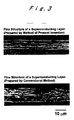
- Fig. 3 is a photograph of the fine structure of a superconducting phase within a wire, after heat treatment according to the present invention, shown in comparison to that obtained by a former method.
- the superconductor is composed mainly of a Bi-type 2212 phase, namely, a Bi 2 Sr 2 CaCu 2 O x phase.
- Other elements may be added or the composition may be finely controlled, as long as the 2212 crystal phase is maintained and the superconductivity is not impaired.
- These superconductors are combined with a metallic substrate, typically silver (Ag) and silver alloy, as in conventional methods.
- the substrate may be chosen from a variety of substances in order to assure ease in processing.
- the Bi-type superconducting composite materials which are obtained by a method containing a baking step, baking is conducted as an isothermal treatment at two stages or more.
- the first baking is not effective at temperatures bellow 700°C. Therefore, it is more favorable to conduct the first baking at a temperature of 700°C or higher, more specifically at a temperature in the range of 700 to 900°C.
- the second baking is more favorable to Conduct the second baking at temperatures in the range of 800 to 900°C.
- the baking time should generally be 10 minutes or more for both the first and second baking steps. It is however, more preferable that the second baking is conducted longer than the first baking, desirably 1 hour or more.
- the partial pressure of oxygen is fixed between 0.1 and 10 atm.
- the oxygen gas used in this process may be mixed with an inert gas such as a rare gas or nitrogen gas.
- the first and second baking may be conducted successively in this order.
- a process where the material is plastic worked may be conducted between the first and second baking.
- the cold working process is effective in improving the characteristics of the wire.
- the gradual cooling of the substrate at a rate of 1 to 10°C/hr after the second baking may be performed for further improvement of the critical current.
- the baking of the composite material may be, for example, a metallic substrate having a material film on its surface which is capable of forming a bismuth (Bi) 2212 superconductive phase, a composite material obtained by further wrapping this substrate with a foil of metallic substrate, or a composite wire obtained by encapsulating a material capable of forming a bismuth (Bi) 2212 superconductive phase into a tube of a metallic substrate.
- the form of the substrate therefore, is not particularly limited.
- the invention is illustrated more specifically by referring to the following Example.
- a silver (Ag) foil was coated with a mixture of an oxide which produces bismuth 2212 superconductive phase (Bi 2 Sr 2 CaCu 2 O x ) by baking and an organic solvent, dried, and subjected to tentative baking to form a thick film.
- This composite film was wrapped with a silver (Ag) foil to provide a wire with an exposed surface of silver (Ag).
- This product was then subjected to a first baking step as an isothermal heat treatment under a stream of pure oxygen gas with a constant concentration at a temperature of 850°C or 880°C for 10 minutes or 1 hour.
- the oxygen partial pressure was 1 atm.
- the product was cooled to room temperature, and cold-plastic worked. This process was conducted once using a pressure roll, and the deformation rate (sectional shrinkage rate) was set at 25%.
- the second baking was conducted as an isothermal heat treatment under a constant stream of pure oxygen gas with a partial pressure of 1 atm, at a temperature in the range of 860 to 880°C for a period of 24 to 100 hours.
- the critical current density of the resulting composite material after the second baking was measured by a direct current four terminal method. Furthermore, the critical current was measured in a magnetic field of 10 T at 4.2K.
- Fig. 1 shows the relationship between the first baking temperature and the critical current.
- the first baking was conducted for 1 hour
- the second baking was conducted at 880°C for 24 hours.
- the critical current value exceeds 400 A.
- the best property, obtained in this experiment was a critical current value of 550 A.
- the critical current was approximately 400 A.
- Fig. 2 shows the relationship between the second baking time and the critical current.
- the first baking was conducted at 888°C for 10 minutes
- the second baking was conducted at 880°C for 24, 48 and 100 hours. It is found that a critical current of approximately 500 A is obtained for the sample baked fore 24 hours. In addition, a critical current exceeding 400 A was obtained for the sample after a treatment of 48 or 100 hours.
- Fig. 3 shows the fine structure of the superconductive phase in a wire subjected to heat treatment.
- a product prepared by the method introduced in the present invention, and a product prepared by a conventional method of partial melting-cooling treatment are shown therein for comparison.
- the present invention provides an oriented particle structure required for excellent properties.
- the degree of particle orientation and the density of the product prepared by the new process resemble those of the related art.
Landscapes
- Engineering & Computer Science (AREA)
- Manufacturing & Machinery (AREA)
- Inorganic Compounds Of Heavy Metals (AREA)
- Superconductors And Manufacturing Methods Therefor (AREA)
- Compositions Of Oxide Ceramics (AREA)
- Superconductor Devices And Manufacturing Methods Thereof (AREA)
Applications Claiming Priority (2)
| Application Number | Priority Date | Filing Date | Title |
|---|---|---|---|
| JP32719798 | 1998-11-17 | ||
| JP10327197A JP3049314B1 (ja) | 1998-11-17 | 1998-11-17 | 酸化物超伝導複合線材の製造方法 |
Publications (2)
| Publication Number | Publication Date |
|---|---|
| EP1003228A2 true EP1003228A2 (de) | 2000-05-24 |
| EP1003228A3 EP1003228A3 (de) | 2002-11-20 |
Family
ID=18196408
Family Applications (1)
| Application Number | Title | Priority Date | Filing Date |
|---|---|---|---|
| EP99309160A Withdrawn EP1003228A3 (de) | 1998-11-17 | 1999-11-17 | Verfahren zur Herstellung eines supraleitenden, Oxyd enthaltenden Materialgemisches |
Country Status (3)
| Country | Link |
|---|---|
| US (1) | US6569813B2 (de) |
| EP (1) | EP1003228A3 (de) |
| JP (1) | JP3049314B1 (de) |
Families Citing this family (3)
| Publication number | Priority date | Publication date | Assignee | Title |
|---|---|---|---|---|
| CN102097184B (zh) * | 2011-02-28 | 2011-12-21 | 西北有色金属研究院 | 一种铋系高温超导材料的制备方法 |
| CN105702388B (zh) * | 2016-04-25 | 2017-03-29 | 西北有色金属研究院 | 一种Bi‑2212超导线/带材的热处理方法 |
| CN105957640B (zh) * | 2016-05-20 | 2017-07-07 | 西北有色金属研究院 | 一种Bi‑2212超导线/带材的制备方法 |
Family Cites Families (3)
| Publication number | Priority date | Publication date | Assignee | Title |
|---|---|---|---|---|
| US5401717A (en) * | 1992-09-28 | 1995-03-28 | General Electric Company | Elongate bismuth system superconductor having aligned 2212 phase |
| DE4445405A1 (de) | 1994-12-20 | 1996-06-27 | Siemens Ag | Verfahren zur Herstellung eines langgestreckten Supraleiters mit einer Bismut-Phase hoher Sprungtemperatur |
| JP2920497B2 (ja) | 1996-06-14 | 1999-07-19 | 工業技術院長 | 超電導テープ材の製造方法 |
-
1998
- 1998-11-17 JP JP10327197A patent/JP3049314B1/ja not_active Expired - Lifetime
-
1999
- 1999-11-17 EP EP99309160A patent/EP1003228A3/de not_active Withdrawn
-
2001
- 2001-01-22 US US09/765,275 patent/US6569813B2/en not_active Expired - Fee Related
Also Published As
| Publication number | Publication date |
|---|---|
| US6569813B2 (en) | 2003-05-27 |
| JP2000156125A (ja) | 2000-06-06 |
| EP1003228A3 (de) | 2002-11-20 |
| US20010007849A1 (en) | 2001-07-12 |
| JP3049314B1 (ja) | 2000-06-05 |
Similar Documents
| Publication | Publication Date | Title |
|---|---|---|
| US5661114A (en) | Process of annealing BSCCO-2223 superconductors | |
| DE3877116T2 (de) | Koerper mit supraleitendem oxid und dessen herstellungsverfahren. | |
| DE3889989T2 (de) | Supraleitende Dünnschicht und Verfahren zu deren Herstellung. | |
| EP0356969A2 (de) | Verfahren zur Herstellung eines oxidischen Supraleiters | |
| DE10212126A1 (de) | Supraleitender Magnesiumdiborid-Dünnfilm und Verfahren und Vorrichtung zu seiner Herstellung | |
| JP2711253B2 (ja) | 超伝導膜及びその形成方法 | |
| US5635456A (en) | Processing for Bi/Sr/Ca/Cu/O-2223 superconductors | |
| US5639714A (en) | Method of producing oxide superconductor | |
| US5354535A (en) | Synthesis of highly phase pure (Bi, Pb)-Sr-Ca-Cu-O superconductor | |
| US6569813B2 (en) | Method of producing oxide superconductive composite material | |
| US5284822A (en) | Oxide superconductor and process for producing the same | |
| US6243598B1 (en) | Method of preparing rare earth-barium cuprates superconductors | |
| JP2920497B2 (ja) | 超電導テープ材の製造方法 | |
| Schartman et al. | Supersolidus Phase Investigation of the Bi‐Sr‐Ca‐Cu Oxide System in Silver Tape | |
| EP0676817B1 (de) | Verfahren zum Herstellen eines supraleitenden Hochtemperaturdrahtes | |
| US5840659A (en) | Method of preparing oxide superconductive material | |
| JP4011130B2 (ja) | 酸化物超電導線材の製造方法 | |
| US6240620B1 (en) | Making of bismuth 2212 superconducting wire or tape | |
| EP0362694B1 (de) | Verfahren zur Herstellung eines oxidischen supraleitenden Drahts | |
| Klein et al. | Plasma Oxidation of Y-Ba-Cu-O Precursor Filaments | |
| JPH03112810A (ja) | 酸化物超伝導膜の作製方法 | |
| JPH06187848A (ja) | 酸化物超伝導線材およびその製造方法 | |
| JPH0412023A (ja) | 酸化物超電導体 | |
| JPH087680A (ja) | 酸化物超伝導線材の製造方法 | |
| JPH09235120A (ja) | Bi基酸化物超電導体の製造方法 |
Legal Events
| Date | Code | Title | Description |
|---|---|---|---|
| PUAI | Public reference made under article 153(3) epc to a published international application that has entered the european phase |
Free format text: ORIGINAL CODE: 0009012 |
|
| AK | Designated contracting states |
Kind code of ref document: A2 Designated state(s): AT BE CH CY DE DK ES FI FR GB GR IE IT LI LU MC NL PT SE |
|
| AX | Request for extension of the european patent |
Free format text: AL;LT;LV;MK;RO;SI |
|
| PUAL | Search report despatched |
Free format text: ORIGINAL CODE: 0009013 |
|
| AK | Designated contracting states |
Kind code of ref document: A3 Designated state(s): AT BE CH CY DE DK ES FI FR GB GR IE IT LI LU MC NL PT SE |
|
| AX | Request for extension of the european patent |
Free format text: AL;LT;LV;MK;RO;SI |
|
| 17P | Request for examination filed |
Effective date: 20030310 |
|
| AKX | Designation fees paid |
Designated state(s): DE DK FR GB |
|
| 17Q | First examination report despatched |
Effective date: 20070309 |
|
| STAA | Information on the status of an ep patent application or granted ep patent |
Free format text: STATUS: THE APPLICATION IS DEEMED TO BE WITHDRAWN |
|
| 18D | Application deemed to be withdrawn |
Effective date: 20070720 |