EP1003196A1 - Kohlenstoffmaterial und Verfahren zur Herstellung, Feldemissionskaltkathode die dieses Material verwendet und Verfahren zur Herstellung - Google Patents
Kohlenstoffmaterial und Verfahren zur Herstellung, Feldemissionskaltkathode die dieses Material verwendet und Verfahren zur Herstellung Download PDFInfo
- Publication number
- EP1003196A1 EP1003196A1 EP99123043A EP99123043A EP1003196A1 EP 1003196 A1 EP1003196 A1 EP 1003196A1 EP 99123043 A EP99123043 A EP 99123043A EP 99123043 A EP99123043 A EP 99123043A EP 1003196 A1 EP1003196 A1 EP 1003196A1
- Authority
- EP
- European Patent Office
- Prior art keywords
- carbon film
- carbon
- film
- acicular
- cold cathode
- Prior art date
- Legal status (The legal status is an assumption and is not a legal conclusion. Google has not performed a legal analysis and makes no representation as to the accuracy of the status listed.)
- Withdrawn
Links
Images


Classifications
-
- H—ELECTRICITY
- H01—ELECTRIC ELEMENTS
- H01J—ELECTRIC DISCHARGE TUBES OR DISCHARGE LAMPS
- H01J1/00—Details of electrodes, of magnetic control means, of screens, or of the mounting or spacing thereof, common to two or more basic types of discharge tubes or lamps
- H01J1/02—Main electrodes
- H01J1/30—Cold cathodes, e.g. field-emissive cathode
- H01J1/304—Field-emissive cathodes
-
- H—ELECTRICITY
- H01—ELECTRIC ELEMENTS
- H01J—ELECTRIC DISCHARGE TUBES OR DISCHARGE LAMPS
- H01J9/00—Apparatus or processes specially adapted for the manufacture, installation, removal, maintenance of electric discharge tubes, discharge lamps, or parts thereof; Recovery of material from discharge tubes or lamps
- H01J9/02—Manufacture of electrodes or electrode systems
-
- C—CHEMISTRY; METALLURGY
- C23—COATING METALLIC MATERIAL; COATING MATERIAL WITH METALLIC MATERIAL; CHEMICAL SURFACE TREATMENT; DIFFUSION TREATMENT OF METALLIC MATERIAL; COATING BY VACUUM EVAPORATION, BY SPUTTERING, BY ION IMPLANTATION OR BY CHEMICAL VAPOUR DEPOSITION, IN GENERAL; INHIBITING CORROSION OF METALLIC MATERIAL OR INCRUSTATION IN GENERAL
- C23C—COATING METALLIC MATERIAL; COATING MATERIAL WITH METALLIC MATERIAL; SURFACE TREATMENT OF METALLIC MATERIAL BY DIFFUSION INTO THE SURFACE, BY CHEMICAL CONVERSION OR SUBSTITUTION; COATING BY VACUUM EVAPORATION, BY SPUTTERING, BY ION IMPLANTATION OR BY CHEMICAL VAPOUR DEPOSITION, IN GENERAL
- C23C16/00—Chemical coating by decomposition of gaseous compounds, without leaving reaction products of surface material in the coating, i.e. chemical vapour deposition [CVD] processes
- C23C16/22—Chemical coating by decomposition of gaseous compounds, without leaving reaction products of surface material in the coating, i.e. chemical vapour deposition [CVD] processes characterised by the deposition of inorganic material, other than metallic material
- C23C16/26—Deposition of carbon only
-
- C—CHEMISTRY; METALLURGY
- C23—COATING METALLIC MATERIAL; COATING MATERIAL WITH METALLIC MATERIAL; CHEMICAL SURFACE TREATMENT; DIFFUSION TREATMENT OF METALLIC MATERIAL; COATING BY VACUUM EVAPORATION, BY SPUTTERING, BY ION IMPLANTATION OR BY CHEMICAL VAPOUR DEPOSITION, IN GENERAL; INHIBITING CORROSION OF METALLIC MATERIAL OR INCRUSTATION IN GENERAL
- C23C—COATING METALLIC MATERIAL; COATING MATERIAL WITH METALLIC MATERIAL; SURFACE TREATMENT OF METALLIC MATERIAL BY DIFFUSION INTO THE SURFACE, BY CHEMICAL CONVERSION OR SUBSTITUTION; COATING BY VACUUM EVAPORATION, BY SPUTTERING, BY ION IMPLANTATION OR BY CHEMICAL VAPOUR DEPOSITION, IN GENERAL
- C23C16/00—Chemical coating by decomposition of gaseous compounds, without leaving reaction products of surface material in the coating, i.e. chemical vapour deposition [CVD] processes
- C23C16/56—After-treatment
-
- H—ELECTRICITY
- H01—ELECTRIC ELEMENTS
- H01J—ELECTRIC DISCHARGE TUBES OR DISCHARGE LAMPS
- H01J2201/00—Electrodes common to discharge tubes
- H01J2201/30—Cold cathodes
- H01J2201/304—Field emission cathodes
- H01J2201/30446—Field emission cathodes characterised by the emitter material
Definitions
- the present invention relates to a carbon material, a method for manufacturing the same material, a field-emission type cold cathode using the same material and a method for manufacturing the same cathode and, more particularly, to a field-emission type cold cathode having an emitter which emits electrons and a method for forming an acicular emitter in a field-emission type cold cathode having emitters which use the carbon material as a carbon film.
- a field-emission type cold cathode is attracting world attention because it can act as an electron gun, in place of a hot cathode, which is capable of emitting electrons in a vacuum by applying an electric field on an emitter.
- attention is given to a cone-shaped emitter having a minute cone shape and a method for using a diamond as an emitter material.
- the cone-shaped emitter having a minute cone shape has come to be able to be made by the recently advanced microlithography for semiconductor devices in sub-micron processing, whereby a minute electron source can be easily formed.
- a material of diamond has a variety of advantages as an electron-emission element such as a large hardness, a chemical stability, and a negative electron affinity that the energy level of a semiconductor surface is lower than that in a vacuum.
- the negative electron affinity of a diamond gives itself such an advantage that when electrons are supplied to the conduction band of the diamond to reach its surface, electrons can be emitted in a vacuum.
- a diamond as an emitter material.
- the surface of a minute electron source formed in a cone is coated with a thin film of diamond or that of such carbon as diamond-like carbon.
- This method has an advantage that a cone-shaped field-emission type cold cathode can be made only by adding a step of depositing a thin film of diamond to a cone tip by a CVD (Chemical Vapor Deposition) method etc.
- CVD Chemical Vapor Deposition
- Another method is also proposed for etching the diamond film itself. It is disclosed in Japanese Laid-Open Patent Application No. Hei6-132254.
- a mask material such as aluminum is formed on the surface of a diamond film and then a mixture gas containing argon and oxygen is used to perform plasma etching on the diamond film selectively.
- This method is advantageous in that it provides a higher selection ratio between a mask material and a diamond, thus giving a higher degree of fine patterning. It is reported also that when this method is employed in plasma etching by use of an oxygen gas, the selection ratio for a mask material becomes indeed even higher but, the diamond surface is degraded in terms of flatness, thus creating a columnar construction of 10-50 nm in size.
- Still another method is disclosed in Japanese Laid-Open Patent application No. Hei9-265892 for forming a diamond film on a protrusion-shaped emitter tip.
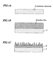
- Figs. 10 are cross-sectional views illustrating sequential steps of a conventional example.
- a substrate electrode consisting of for example a silicon substrate
- a protrusion-shaped conductive material 8 made of for example silicon
- a tip of which is formed a diamond This manufacturing method is described below along the sequence of steps.
- a substrate electrode 1 is provided with a diamond film 6 formed thereon using a CVD method.
- an aluminum layer 7 which acts as a mask for processing the diamond is formed by a vacuum evaporation method.
- Fig. 10A a substrate electrode 1 is provided with a diamond film 6 formed thereon using a CVD method.
- an aluminum layer 7 which acts as a mask for processing the diamond is formed by a vacuum evaporation method.
- a photolithographic method is used to etch a photo-resist into such a desired pattern as having for example a five-micron diameter and a 20micron spacing, which is in turn used as a mask to pattern the aluminum layer 7.
- the diamond 6 is patterned by means of reactive ion etching using an oxygen gas.
- the aluminum layer 7 is removed and then, using the diamond 6 as a mask, the substrate electrode 1 is etched by reactive ion etching, to form a protrusion-structured conductive material 8.
- Still another method comprises a step of forming a nano-fiber made of graphite grown selectively, which is disclosed in pages 2119-2121 of volume 73, number 15 of the Applied Physic Letters published in 1998.
- a plasma-assisted CVD method is performed on a substrate made of nickel, to cause fiber-like graphite to grow on the substrate. It is reported that by this method, a nano-fiber measuring 30-100 nm in size is formed.
- a first problem of the conventional technology shown in Figs. 10 is that since a cone-shaped emitter is formed and then such a carbon film as made of a diamond is coated on that, the radius of curvature of the tip of the emitter is rather large, thus being disadvantageous in the emission of electrons.
- the field-emission properties in general depend largely on the radius of curvature and work function of the tip of the emitter material. With this, therefore, even when a diamond or the like material liable to emit electrons is coated on the surface of a con-shaped emitter, the radius of curvature of the tip is increased by as much as the thickness of the coated film. As a result, although the emission performance is improved by the coating material, the radius of curvature of the tip becomes large, thus offsetting and limiting the emission performance.
- a second problem of the conventional technology is that since an oxygen gas is mainly used as an etching gas for a diamond, the diamond surface is liable to be oxygen-terminated.
- An oxygen gas has indeed an advantage that it has a higher etching rate as compared to a diamond and also a high selection ratio as compared to aluminum etc. as a mask material.
- the diamond surface has an oxygen-terminated construction, so that it cannot enjoy negative electron-affinity properties that can be obtained with hydrogen termination, thus being degraded in terms of emission performance, which leads to a problem.
- the diamond surface when hydrogen-terminated, has higher conductivity and is easy to supply emission electrons for to the tip of an emitter, the oxygen-terminated surface supply those electrons via a diamond bulk with a lower conductivity to the emitter tip, thus being rendered disadvantageous in obtaining of a large emission current when the emitter is formed only of a diamond.
- the third problem is that although a diamond which is processed using an oxygen gas as a main etching gas provides a higher selection ratio with a mask material, a columnar structure created inherently makes it difficult to apply an electric field on a protrusion-shaped tip of an emitter.
- the emission properties largely depend on the radius of curvature of the emitter tip, it is advantageous for the better emission properties to have a small shape of a sharp tip with a small radius of curvature.
- oxygen is used in etching in fact, a columnar structure is given a flat shape of the tip, which is advantageous in emission.
- the fourth problem is that since the emitter is shaped in such a manner that a protrusion-shaped emitter may be formed with a material rather easy to form, thus depositing a diamond on the tip, the shape of a diamond formed on the tip is determined by a photolithographic method of forming a diamond, thereby making it difficult to fine-pattern the tip and reduce an inter-emitter distance.
- the fine patterning limits by photography is considered to be a sub-micron order for the diamter and the inter-pattern distance.
- This conventional technology therefore, can give a radius of curvature of the tip which is only 10 times or more as large as about 10 nm, which is given by a cone-shaped minute emitter, thus being disadvantageous in emission.
- the inter-emitter distance is restricted, thus limiting the improvements in the performance of emission.
- the fifth problem is that the method of forming a nano-fiber brings about an acicular emitter consisting of a graphite fiber, so that only a graphite quality of film can be obtained, thus making it impossible in some cases to obtain a negative electron affinity that can be obtained with a diamond. Furthermore, the shape is limited to a fiber construction, so that although a diameter of tip of about 30 nm at the minimum can be obtained, only a diameter of about 60-70 nm is mainly obtained, thus restricting the micro-processing of the tip.
- a carbon material wherein a surface of a carbon film is covered with an acicular protrusion structure made of carbon.
- a preferable mode is one wherein the carbon film surface is covered with an acicular protrusion-shaped structure made of carbon.
- a method for manufacturing a carbon material which comprises a step of performing plasma processing on a carbon film in an atmosphere of hydrogen, to form an acicular carbon film on a surface of said carbon film.
- a preferable mode is one wherein a method for manufacturing a carbon material comprises a step of performing plasma processing in an atmosphere of oxygen before or after said step of performing plasma processing in an atmosphere of hydrogen.
- a preferable mode is one wherein the method for manufacturing a carbon material comprises a step of etching said carbon film during said plasma processing, to form an acicular carbon film.
- a preferable mode is one wherein the method for manufacturing a carbon material comprises a step of forming a material with a different etching rate in or on a surface of said carbon film during the plasma processing in an atmosphere of hydrogen, to use that material with a low etching rate as a mask during the etching of that carbon film, thus making it possible to form an acicular emitter in a self-alignment manner.
- a preferable mode is one wherein the method for manufacturing a carbon material comprises a step of forming said carbon film in such a way that said carbon film may have an sp2 structure and an sp3 structure mixed therein.
- a preferable mode is one wherein said plasma processing is performed using ECR (Electron Cyclotron Resonance) plasma.
- a preferable mode is one wherein said ECR plasma processing is performed with a bias being applied to a substrate in a processing apparatus.
- a field-emission type cold cathode having a carbon material according to the first aspect as an emitter.
- a method for manufacturing a field-emission type cold cathode which comprises a step of forming an acicular protrusion structure which provides an emitter, using said method for manufacturing a carbon material according to the third aspect.
- a diamond film having better emission performance i.e. sp3-sturctured carbon film
- a graphite film having higher conductivity i.e. sp2-structured carbon film
- This configuration provides even better emission properties by arranging an sp3-structured carbon film on the emitter tip.
- hydrogen plasma processing when performed, makes it possible to cover the surface of an acicular emitter with an amorphous carbon film or an preferably an sp2-structured conductive film made of carbon so as to form a field-emission type cold cathode having higher conductivity.
- a field-emission type cold cathode with higher conductivity can be formed.
- a first embodiment of the present invention has such a construction that on a substrate electrode 1 which provides a conductive cathode electrode, a carbon film 2 is formed which is covered, on its upper surface, with a sharp and acicular protrusion-shaped structure.
- This acicular protrusion-shaped structure has a cone or pyramid shape with a bottom-surface width of from a few to 200 nm and a height of from about 10 nm to 1 ⁇ m disposed with almost the same pitch as the bottom-surface width.
- a manufacturing method is described as follows.
- a substrate electrode 1 for example an n-type silicon substrate is provided as a substrate electrode 1.
- this substrate is made of silicon, any appropriate substrate electrode made of other materials may be used such as one having metal formed on its glass substrate in an application field of, for example, display.
- the carbon film 2 is deposited as thick as about 5 ⁇ m using a hot-filament CVD method.
- diamond powders with a grain diameter of about 1 ⁇ m are attached onto the surface of the substrate electrode 1 by performing scratch processing, which electrode 1 is in turn placed in a hot-filament CVD chamber which is exhausted down to about 10 -6 Torr, into which is then introduced for example methane/hydrogen at a flow rate of about 5 sccm/500 sccm, to form the carbon film at a pressure of 20 Torr.
- the filament temperature is about 2200°C and the substrate temperature is about 800°C.
- hydrogen is introduced at a flow rate of about 40 sccm to perform such processing that ECR plasma with a power of about 500 watts is generated by applying a magnetic field of about 850-900 gausses and a microwave having a frequency of about 2.5 GHz to an ECR ion source at a pressure of from about 10 -4 to 10 -3 Torr.
- the carbon film is provided on its surface with acicular structures formed close to each other.
- This acicular structure is made because such phenomenon occur independently or in a composite manner as one that by the ECR plasma processing, a structure of the carbon film or a deposition on its surface or a re-grown product acts as a mask for etching the carbon film and another that the carbon film changes in shape selectively because of a difference in surface orientation of the carbon film or etching rate for the grains of the polycrystalline structure.
- the present invention has another advantage that etching according to the present invention does not use as the main etchant component an argon gas having an etching rate irrespective of the material, to prevent rapid removal of the mask material in etching, thus resulting in the formation of protrusions with a high aspect ratio.
- the present invention does not employ as the main etchant component an oxygen gas with a high selection ratio, thus preventing the formation of a columnar structure other than an acicular structure and also avoiding the removal, by etching, of the carbon film before the formation of an acicular structure because the etching rate is not so high as with oxygen.
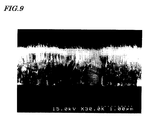
- Fig. 9 shows a photograph of the carbon film after being etched.
- the second embodiment of the present invention has such a construction that on a substrate electrode 1 which provides a conductive cathode electrode is formed a carbon film 2 which is covered on its upper surface with a protrusion-shaped structure, on the tip of which film 2 is formed an sp3-structured carbon 3 having a sharp shape.
- the protrusion-shaped structure has a cone or pyramid shape having a bottom surface width of from several to 200 nm and a height of from about 10 nm to 1 ⁇ m.
- This sp3-structured carbon 3 has a radius of curvature of 100 nm or less, preferably 10 nm or so. This is because the emission properties of an acicular emitter largely depends on the radius of curvature of the tip. Moreover, when the carbon film 2 is of an sp2 structure, low-resistance graphite-like properties can be obtained, thus being advantageous in supplying of an electric current to the tip of an acicular structure which acts as an emission point as compared to a case where the carbon film 2 is of an sp2 structure.
- a manufacturing method is described as follows.
- Fig. 2A for example on the substrate electrode 1.
- the carbon film 2 is formed as thick as about 5 ⁇ m by for example a hot-filament CVD method.
- Fig. 2B a grain-like sp3-structured carbon 3 is formed on the surface of the carbon film 2 by for example scratching a diamond.
- Fig. 2C ECR plasma processing by use of a hydrogen gas is performed, to etch the carbon film 2 using the sp3-structured carbon film 3 as a mask.
- this step by using an sp3-structured graphite film in place of the carbon film 2, it is possible to obtain an appropriate value of selection ratio with the sp3-structured surface carbon film and also to obtain such an acicular shape as leaving the sp3-structured carbon film 3 on the tip because as the carbon film 2 is etched in a depth direction, the sp3-structured carbon 3 is also etched in reduced in area.
- the present embodiment makes it possible to selectively form, in an easy manner, the tips of acicular emitters arranged in a uniform height of an sp3-structured diamond with large emission-current properties.
- a hot-filament CVD method may be performed at a substrate temperature of about 600°C to form a carbon film on the surface of the carbon film 2, thus resulting in sp2 and sp3 structures being mixed in the carbon film.
- sp3-structured carbon in this film may be used as a mask.
- the third embodiment of the present invention has such a construction that on a substrate electrode 1 which provides a conductive cathode electrode is formed a carbon film 2 which is covered on its upper surface with a protrusion-shaped structure and which contains sp3-structured carbon 3. Also, as shown in the figure, the sp3-structured carbon 3 may be arranged at the tip of an acicular protrusion which provides an emitter.
- the protrusion-shaped structure is of a cone or pyramid shape, having its bottom surface width from of a few to 200 nm of and a height of from about 10 nm to 1 ⁇ m and being arranged with almost the same pitch as the bottom surface width therebetween.
- the carbon film 2 in this embodiment is mainly of an sp2 structure.
- the carbon film 2 in this embodiment is mainly of an sp2 structure.
- the tip of the acicular structure made of an sp3-structured carbon film diamond-like emission properties can be obtained.
- a manufacturing method is described as follows.
- the carbon film 2 is etched in ECR plasma processing by use of a hydrogen gas.
- a half-way shape in the ECR plasma processing is, as shown in Fig.
- the carbon film 2 is gradually etched, during which the sp3-structured carbon 3 contained in the film is exposed and then acts as a mask because of its low etching rate, thus forming an acicular protrusion.
- the ECR plasma conditions or the film properties so as to obtain an appropriate selection ratio, it is possible to obtain such an acicular shape with the sp3-structured carbon film 3 left at the tip because the carbon film is etched in the depth direction and, at the same time, the sp3-structured carbon film 3 is also etched and reduced in size.
- the sp3-structured carbon film 3 formed deep in the carbon film 2 is exposed as shown in Fig. 3C, which then acts as a mask to form the acicular protrusion. With this, a number of the acicular protrusions with different heights is formed everywhere in the surface.
- this method is capable of removing the sp3-structured carbon film 3 by elongating the ECR plasma processing in time. It is also possible to adjust the height of the acicular protrusion by adding oxygen-plasma processing. It is preferably also that the grain diameter of the sp3-structured carbon 3 contained in the carbon film be finally 10 nm or less in order to determine the diameter of the emitter tip. To form an acicular protrusion having an aspect ratio of 10 or higher, the selection ratio must be 10 or so. If, in this case, the sp3-structured carbon 3 is to be etched in an isotropic manner in the ECR plasma processing, its grain diameter must be that of the emitter tip multiplied by the selection ratio. Therefore, it is preferably 100 nm or so.
- This method has such an advantage that when the carbon film 2 is being formed, the sp3-structured carbon 3 can also be formed simultaneously which acts as a mask for forming an acicular protrusion in the film, thus reducing the number of steps required. Moreover, the sp3-structured carbon 3 contained in the film can be used as a mask to arrange the sp3-structured carbon film 3 having large emission-current properties at the acicular protrusion, i.e. emitter tip in a self-alignment manner.
- the sp3-structured carbon 3 is arranged which acts as a mask for forming an acicular protrusion also in the depth direction of the carbon film 2, to enable forming an acicular protrusion also between the existing acicular protrusions, thus largely improving the in-surface density of acicular protrusions.
- a fourth embodiment of the present invention is described as follows.
- a substrate electrode 1 which provides a conductive cathode electrode is formed a carbon film 2 covered on its upper surface with a protrusion structure having a height of for example about 1 ⁇ m, on which is formed a gate electrode 5 made of a metal film with a thickness of about 200 nm via an insulator film 4 consisting of an oxide film with a thickness of for example about 800 nm.
- a carbon film 3 having an acicular protrusion which provides an emitter is shown according to the first embodiment of the present invention, it is not restricted to the first embodiment but such an emitter as according to the second or third embodiment may be employed.
- the gate electrode 5 is arranged in the vicinity of an emitter, thus making it possible to apply a desired electric field on the tip of the emitter at a low voltage for easily obtaining higher emission properties.
- FIG. 5D shows a cross-sectional view of a field-emission type cold cathode device according to the fifth embodiment of the present invention.
- a substrate electrode 1 is a material which serves as a base when a cold cathode material is deposited, acting also as a lower electrode.
- the substrate electrode 1 used in the fifth embodiment may be made of a semiconductor substance or any conductor such as for example Si, Mo, Fe, Ni, or Pt. Also, a glass-like insulating substrate on which a metal film is attached, evaporated, or deposited may be used as a substrate electrode.
- a carbon film 2 which provides a cold cathode material is provided for emitting electrons.
- This carbon film 2 has n acicular protrusion-structured surface.
- a surface conductive film 9 consists of a carbon film containing an sp2 structure, having high conductivity as compared to the carbon film 2, as well as a thickness of 10 nm or less and a surface resistivity of 10 5 ⁇ cm or less.
- the surface conductive film 9 constitutes part of a path for supplying electrons, so preferably has a low resistivity, for example 10 5 ⁇ cm or less.
- An insulator film 4 is an insulating material which electrically isolates the carbon film 2 and a gate electrode 5 from each other, consisting mainly of an oxide film etc.
- the gate electrode 5 is provided to draw electrons, consisting of a metal thin film.
- an n-type silicon substrate is used as the substrate electrode 1.
- a polycrystalline diamond as the carbon film 2 using a CVD method.
- the surface of the carbon film 2 is exposed to hydrogen plasma.
- This hydrogen plasma processing generated is of an ECR type. In this processing, impurities and minute defects present in the CVD-polycrystalline diamond film are selectively etched, thereby resulting in an acicular structure.
- This method need not use a lithographic step for processing a cold cathode material itself.
- the step of etching hydrogen plasma damages the carbon film 2, thus forming the surface conductive film 9 consisting of an amorphous carbon film or preferably a carbon film containing an sp2 structure both on the surface of the carbon film 2 and on the surface of the acicular protrusion structure.
- the insulator film 4 and the gate electrode 5 are patterned into a desired shape performing a lithographic step.
- hydrogen plasma processing alone is performed to form an acicular structure
- oxygen plasma processing may be performed before the hydrogen plasma processing.
- an acicular protrusion structure can be formed by hydrogen plasma processing with the carbon film 2 being reduced thinner, thus easily forming causing an acicular protrusion structure to grow on the surface of the substrate electrode 2, which is an advantage of the present invention.
- the above-mentioned procedure forms the insulator film and the gate electrode after giving an acicular structure to the carbon film 2 using hydrogen plasma, the insulator film 4 and the gate electrode 4 may be formed first and then the carbon film 2 may be processed into an acicular structure.
- the carbon film 2 below the insulator film 4 is formed as reduced acicular
- the acicular shape of the carbon film 4 below the insulator film 4 may be removed beforehand by oxygen plasma etching etc. to provide a flattened structure, before the insulator film 4 is formed thereon.
- a field-emission type cold cathode according to the fifth embodiment of the present invention In detail with reference to Fig. 5D.
- a negative bias or a positive bias is applied to the substrate electrode 1 or the gate electrode 5 respectively.
- an electric field is concentrated at the tip of the carbon film 2 rendered acicular protrusion-structured, thus making it possible to decrease the voltage to be applied to the substrate electrode 1 or the gate electrode 5.
- Table 1 lists the threshold field strength of an as-grown diamond film (sample 1) before hydrogen plasma processing, another diamond film (sample 2) covered with a diamond film which has an acicular structure on its surface caused by hydrogen plasma processing and which contains in its surface an sp2 structure, and still another diamond film (sample 3) obtained by removing this carbon film containing the sp2 structure by oxidizing agent or oxygen plasma.
- a reference current density employed in this case is 10 ⁇ A/cm 2 . Based on the results, it is found that sample 2 has the lowest threshold field strength, with improved field-emission properties.
- sample 1 sample 2 sample 3 threshold field strength 120V/ ⁇ m 1V/ ⁇ m 7V/ ⁇ m
- FIG. 6D is a cross-sectional view of the sixth embodiment of the present invention.
- a substrate electrode 1 constitutes a lower electrode.
- This substrate electrode 1 may be made of a semiconductor substance or any conductor such as for example Si, Fe, Ni, or Pt.
- a carbon film 2 consists of a cathode material, preferably containing sp3-structured carbon. This carbon film 2 has an acicular protrusion-shaped structure on its surface.
- a surface conductive film 9 consists of an amorphous carbon film or preferably a carbon film containing an sp2 structure, having high conductivity as compared to the carbon film 2 as well as a thickness of 10 nm or less and a surface resistivity of 10 5 ⁇ cm or less. Since the surface conductive film 9 is part of a path for supplying electrons, its resistivity is preferably low, for example 10 5 ⁇ cm.
- An insulator film 4 consists of an insulating material mainly made of an oxide film etc., for electrically isolating the carbon film 2 and the gate electrode 5. The gate electrode 5 is provided for drawing electrons from the carbon film 2, consisting of a metal thin film.
- a support substrate 10 constitutes a base for the field-emission type cold cathode, being made of such an insulating material as glass, plastic, ceramic, etc.
- the carbon film 2 containing for example a polycrystalline diamond as the cold cathode material using a CVD method.
- the carbon film 2 is formed to a film thickness of about 5 ⁇ m.
- an oxide film which provides the insulator film 4 and a metal film which provides the gate electrode 5 are deposited.
- the insulator film 4 and the gate electrode 5 are processed into an arbitrary shape performing a lithographic step.
- the surface of the carbon film 2 is exposed to hydrogen plasma.
- the acicular protrusion structure may reach the surface of the substrate electrode 1 from the surface of the carbon film 2.
- Another configuration may be given such that part of the surface of the substrate electrode 1 may be over-etched.
- the insulator film 4 and the gate electrode 5 are formed on the carbon film 2, which then undergoes hydrogen plasma processing to form an acicular structure
- the carbon film 2 may beforehand undergo hydrogen plasma processing to provide the acicular structure, thereby subsequently forming the insulator film 4 and the gate electrode 5.
- the support substrate 10 which provides the support base is laminated to the back side of the substrate electrode 1.
- a field-emission type cold cathode according to the sixth embodiment of the present invention is described in detail with reference to fig. 6D.
- a negative bias or a positive bias is applied to the substrate electrode 1 or the gate electrode 5 respectively.
- an electric field is concentrated at the tip of the carbon film 2 the surface of which is rendered acicular protrusion-shaped and, at the same time, that acicular protrusion portion has reached the substrate electrode 1, so that electrons can be easily supplied from the substrate, thus decreasing the voltage to be applied to the substrate electrode 1 or the gate electrode 5.
- Fig. 7D shows a cross-sectional view of a field-emission type cold cathode according to the seventh embodiment of the present invention.
- a substrate electrode 1 is a substance which provides a base for depositing a cold cathode material, acting also as a lower electrode.
- This substrate electrode 1 maybe made of a semiconductor substance or any conductor such as for example Si, Mo, Fe, Ni, or Pt. Also, as the substrate, such a glass-like semiconductor substrate may be used on which a metal film is attached, evaporated, or deposited.
- the carbon film 2 which provides the cold cathode material is provided for emitting electrons.
- This carbon film 2 is a cathode material for emitting electrons, comprising sp3-structured carbon 3 and sp2-structured carbon 2a.
- the carbon film 2 has an acicular protrusion-structured surface.
- a surface conductive film 9 consists of an amorphous carbon film or preferably a carbon film containing an sp2 structure, having high conductivity as compared to the carbon film 2 as well as a thickness of 10 nm or less and surface resistivity of 10 5 ⁇ cm less. Since the surface conductive film 9 is part of a path for supplying electrons, its resistivity is preferably low, for example 10 5 ⁇ cm.
- the insulator film 4, mainly formed with an oxide film etc., is an insulating material which electrically isolates the carbon film 2 and the gate electrode 5.
- the gate electrode 5 is provided to draw electrons from the carbon film 2, consisting of a metal thin film.
- an n-type silicon substrate is used as the substrate electrode 1.
- the carbon film 2 is formed using a CVD method or sputtering method.
- a diamond-like carbon film is formed, to a supposed thickness of 3 ⁇ m, as the carbon film 2 which is the cold cathode material.
- This carbon film has the sp2-structured carbon 2a which is dotted therein with sp3-structured carbon 3.
- the surface of the carbon film 2 is exposed to hydrogen plasma.
- Fig. 7C the surface of the carbon film 2 is exposed to hydrogen plasma.
- the sp3-structured carbon 3 acts as a mask to selectively etch the sp2-structured carbon 2a, thus providing an acicular protrusion structure. This is because a strong bonding strength of the sp3 structure as compared to that of the sp2 structure causes selective etching to occur.
- the surface conductive film 9 consisting of an amorphous carbon film or preferably a carbon film containing an sp2 structure is formed on both the surface of the carbon film 2 and the surface of the acicular protrusion structure. Then, as shown in Fig. 7D, the insulator film 4 and the gate electrode 5 are selectively formed.
- the insulator film 4 consists of a metal thin film, to draw electrons from the carbon film 2.
- the acicular protrusion structure of the carbon film 2 has, in the present embodiment, such a shape that the carbon film 2 is left on the base, the acicular protrusion structure may be formed directly from the substrate electrode 1.
- a negative bias or a positive bias is applied to the tip of the substrate electrode 1 or the gate electrode 5 respectively.
- an electric field is concentrated at the tip of the carbon film 2 the surface of which is rendered acicular protrusion-shaped and, at the same time, the surface of the acicular portion of the carbon film 2 is covered with the surface conductive film 9, so that electrons can be supplied from the substrate easily, making it possible to decrease the voltage to be applied to the substrate electrode 1 or the gate electrode 5.
- Fig. 8D is a cross-sectional view of a field-emission type cold cathode given in the eighth embodiment of the present invention.
- a substrate electrode 1, which constitutes a lower electrode may be made of a semiconductor substance or any conductor such as for example Si, Mo, Fe, Ni, or Pt.
- a carbon film 2 which provides a cold cathode material is provided for emitting electrons.
- This carbon film 2 is a cathode material for emitting electrons, comprising an sp2-structured carbon 2a and an sp3-structured carbon 3. Also, this carbon film 2 has an acicular protrusion-structured surface.
- a surface conductive film 9 consists of a carbon film containing an sp2 structure, having high conductivity as compared to the carbon film 2 as well as a thickness of 10 nm or less and a surface resistivity of 10 5 ⁇ cm or less. Since the surface conductive film 9 is part of a path for supplying electrons, its resistivity is preferably low for example 10 5 ⁇ cm or less. Therefore, rather than an sp2-structured carbon film, an amorphous carbon film is preferably, and even more preferably a low-resistivity sp2-structured carbon film is employed.
- An insulator film 4, mainly formed with an oxide film etc., is an insulating material which electrically isolates the carbon film 2 and gate electrode 5.
- a support substrate 10 constitutes a base for the field-emission type cold cathode device, being made of such an insulating material as glass, plastic, or ceramic.
- the support substrate 10 is made of glass, on which is deposited Mo using a sputtering method which provides the substrate electrode.
- the carbon film 2 is formed on this substrate electrode 1 using a CVD or sputtering method.
- a diamond-like carbon film is formed as a cold cathode material on the substrate electrode 1, to a supposed thickness of 3 ⁇ m.
- the carbon film 2 has such a film construction that mixes therein sp2-structured carbon 2 and sp3-structured carbon 3. Then, as shown in Fig.
- an oxide film which provides the insulator film 4 and a metal film which provides the gate electrode 5 are deposited and then, an insulator film 4d and a gate electrode 5d are processed into an arbitrary shape by performing a lithographic step. Then, as shown in Fig. 8D, the surface of a cold cathode material 2d is exposed to hydrogen plasma. In this step of exposure, the sp3-structured carbon 3 acts as a mask to selectively etch the sp2-structured carbon 2a into an acicular protrusion structure.
- the surface conductive film 9 consisting of a carbon film which contains an sp2 structure is formed on the surface of the carbon film 2 and the surface of the acicular protrusion structure.
- a field-emission type cold cathode device according to the eighth embodiment of the present invention is described in detail with reference to Fig. 8D as follows.
- a negative bias or a positive bias is applied to the substrate electrode 1 or the gate electrode 5 respectively.
- an electric field is concentrated at the tip of the carbon film 2 the surface of which is rendered acicular protrusion-shaped and, at the same time, that acicular protrusion portion has reached the substrate electrode 1, so that electrons can be supplied from the substrate easily, thus making it easy to decrease the voltage to be applied to the substrate electrode 1d or the gate electrode 4d.
- a field-emission type cold cathode according to the present invention has such an effect that can easily achieve large emission-current properties even at a low voltage.
- a carbon film which combines therein a diamond film with high emission performance, i.e. sp3-structured carbon film, and a graphite film with high conductivity, i.e. sp2-structured carbon film it is possible to increase both the conductivity and the emission performance.
- the emitter performance can be improved even more.
- the present invention it is possible to provide a method for manufacturing such a field-emission type cold cathode that can achieve large emission-current properties easily. This is because the carbon film can undergo plasma processing, to easily form a plurality of sharp and acicular emitters at the same time.
- the material with lower etching rate can act as a mask when the carbon film is being etched, thus forming acicular emitters in a self-alignment manner.
- the sp2-structured film makes it easy to supply electrons to the tip of the acicular structure.
Landscapes
- Chemical & Material Sciences (AREA)
- Engineering & Computer Science (AREA)
- General Chemical & Material Sciences (AREA)
- Chemical Kinetics & Catalysis (AREA)
- Materials Engineering (AREA)
- Mechanical Engineering (AREA)
- Metallurgy (AREA)
- Organic Chemistry (AREA)
- Manufacturing & Machinery (AREA)
- Inorganic Chemistry (AREA)
- Cold Cathode And The Manufacture (AREA)
Applications Claiming Priority (2)
| Application Number | Priority Date | Filing Date | Title |
|---|---|---|---|
| JP34653898 | 1998-11-19 | ||
| JP34653898 | 1998-11-19 |
Publications (1)
| Publication Number | Publication Date |
|---|---|
| EP1003196A1 true EP1003196A1 (de) | 2000-05-24 |
Family
ID=18384108
Family Applications (1)
| Application Number | Title | Priority Date | Filing Date |
|---|---|---|---|
| EP99123043A Withdrawn EP1003196A1 (de) | 1998-11-19 | 1999-11-19 | Kohlenstoffmaterial und Verfahren zur Herstellung, Feldemissionskaltkathode die dieses Material verwendet und Verfahren zur Herstellung |
Country Status (2)
| Country | Link |
|---|---|
| EP (1) | EP1003196A1 (de) |
| KR (1) | KR20000035592A (de) |
Cited By (3)
| Publication number | Priority date | Publication date | Assignee | Title |
|---|---|---|---|---|
| WO2009113063A2 (en) * | 2008-03-10 | 2009-09-17 | Yeda Research & Development Company Ltd. N | Method for fabricating nano-scale patterned surfaces |
| RU2484548C1 (ru) * | 2011-11-09 | 2013-06-10 | Равиль Кяшшафович Яфаров | Способ изготовления матрицы многоострийного автоэмиссионного катода на монокристаллическом кремнии |
| WO2014007680A2 (ru) * | 2012-07-04 | 2014-01-09 | Evlashin Stanislav Aleksandrovich | Трёхмерно-структурированная полупроводниковая подложка для автоэмиссионного катода, способ ее получения и автоэмиссионный катод |
Families Citing this family (1)
| Publication number | Priority date | Publication date | Assignee | Title |
|---|---|---|---|---|
| KR100743345B1 (ko) * | 2005-01-18 | 2007-07-26 | 미합중국 더 세크리터리 오브 디 에어 포스 | 필드 방출 냉음극 |
Citations (13)
| Publication number | Priority date | Publication date | Assignee | Title |
|---|---|---|---|---|
| JPS524163A (en) * | 1976-03-08 | 1977-01-13 | Hitachi Ltd | Electric field radiation cathode |
| US4143292A (en) * | 1975-06-27 | 1979-03-06 | Hitachi, Ltd. | Field emission cathode of glassy carbon and method of preparation |
| FR2420203A1 (fr) * | 1978-03-13 | 1979-10-12 | Max Planck Gesellschaft | Cathode a emission par effet de champ ainsi que procede de fabrication et utilisation de celle-ci |
| US4957591A (en) * | 1988-03-29 | 1990-09-18 | National Institute For Research In Inorganic Materials | Method for preparing needle-like, fibrous or porous diamond, or an aggregate thereof |
| JPH02239192A (ja) * | 1989-03-10 | 1990-09-21 | Idemitsu Petrochem Co Ltd | ダイヤモンドの合成方法 |
| EP0413834A1 (de) * | 1989-03-10 | 1991-02-27 | Idemitsu Petrochemical Co. Ltd. | Mit diamanten bedecktes glied und verfahren zur herstellung |
| US5010249A (en) * | 1988-09-13 | 1991-04-23 | Seiko Instruments Inc. | Diamond probe and forming method thereof |
| WO1995022168A1 (en) * | 1994-02-14 | 1995-08-17 | The Regents Of The University Of California | Diamond-graphite field emitters |
| EP0718864A1 (de) * | 1994-12-22 | 1996-06-26 | AT&T Corp. | Feldemissionsvorrichtung mit ultrafeinen Diamantteilchen-Emittoren |
| US5703435A (en) * | 1992-03-16 | 1997-12-30 | Microelectronics & Computer Technology Corp. | Diamond film flat field emission cathode |
| EP0836217A1 (de) * | 1996-10-14 | 1998-04-15 | Hamamatsu Photonics K.K. | Elektronenröhre |
| US5844252A (en) * | 1993-09-24 | 1998-12-01 | Sumitomo Electric Industries, Ltd. | Field emission devices having diamond field emitter, methods for making same, and methods for fabricating porous diamond |
| EP0967844A1 (de) * | 1998-06-24 | 1999-12-29 | Commissariat A L'energie Atomique | Verfahren zur ECR-Plasma Beschichtung von elektronenemittierenden Kohlenstoff-Filmen unter Einwirkung eines elektrischen Feldes |
-
1999
- 1999-11-19 EP EP99123043A patent/EP1003196A1/de not_active Withdrawn
- 1999-11-19 KR KR1019990051582A patent/KR20000035592A/ko not_active Application Discontinuation
Patent Citations (13)
| Publication number | Priority date | Publication date | Assignee | Title |
|---|---|---|---|---|
| US4143292A (en) * | 1975-06-27 | 1979-03-06 | Hitachi, Ltd. | Field emission cathode of glassy carbon and method of preparation |
| JPS524163A (en) * | 1976-03-08 | 1977-01-13 | Hitachi Ltd | Electric field radiation cathode |
| FR2420203A1 (fr) * | 1978-03-13 | 1979-10-12 | Max Planck Gesellschaft | Cathode a emission par effet de champ ainsi que procede de fabrication et utilisation de celle-ci |
| US4957591A (en) * | 1988-03-29 | 1990-09-18 | National Institute For Research In Inorganic Materials | Method for preparing needle-like, fibrous or porous diamond, or an aggregate thereof |
| US5010249A (en) * | 1988-09-13 | 1991-04-23 | Seiko Instruments Inc. | Diamond probe and forming method thereof |
| EP0413834A1 (de) * | 1989-03-10 | 1991-02-27 | Idemitsu Petrochemical Co. Ltd. | Mit diamanten bedecktes glied und verfahren zur herstellung |
| JPH02239192A (ja) * | 1989-03-10 | 1990-09-21 | Idemitsu Petrochem Co Ltd | ダイヤモンドの合成方法 |
| US5703435A (en) * | 1992-03-16 | 1997-12-30 | Microelectronics & Computer Technology Corp. | Diamond film flat field emission cathode |
| US5844252A (en) * | 1993-09-24 | 1998-12-01 | Sumitomo Electric Industries, Ltd. | Field emission devices having diamond field emitter, methods for making same, and methods for fabricating porous diamond |
| WO1995022168A1 (en) * | 1994-02-14 | 1995-08-17 | The Regents Of The University Of California | Diamond-graphite field emitters |
| EP0718864A1 (de) * | 1994-12-22 | 1996-06-26 | AT&T Corp. | Feldemissionsvorrichtung mit ultrafeinen Diamantteilchen-Emittoren |
| EP0836217A1 (de) * | 1996-10-14 | 1998-04-15 | Hamamatsu Photonics K.K. | Elektronenröhre |
| EP0967844A1 (de) * | 1998-06-24 | 1999-12-29 | Commissariat A L'energie Atomique | Verfahren zur ECR-Plasma Beschichtung von elektronenemittierenden Kohlenstoff-Filmen unter Einwirkung eines elektrischen Feldes |
Non-Patent Citations (4)
| Title |
|---|
| CHERNOZATONSKII L A ET AL: "ELECTRON FIELD EMISSION FROM NANOFILAMENT CARBON FILMS", CHEMICAL PHYSICS LETTERS,NL,AMSTERDAM, VOL. 233, NR. 1, PAGE(S) 63-68, XP000614463 * |
| KAMIJO E ET AL: "AFM observations of DLC films prepared by the ECR sputtering method", NUCLEAR INSTRUMENTS & METHODS IN PHYSICS RESEARCH, SECTION - B: BEAM INTERACTIONS WITH MATERIALS AND ATOMS,NL,NORTH-HOLLAND PUBLISHING COMPANY. AMSTERDAM, VOL. 121, NR. 1, PAGE(S) 110-115, ISSN: 0168-583X, XP004057886 * |
| PATENT ABSTRACTS OF JAPAN vol. 001, no. 063 (E - 025) 20 June 1977 (1977-06-20) * |
| PATENT ABSTRACTS OF JAPAN vol. 014, no. 559 (C - 0787) 12 December 1990 (1990-12-12) * |
Cited By (7)
| Publication number | Priority date | Publication date | Assignee | Title |
|---|---|---|---|---|
| WO2009113063A2 (en) * | 2008-03-10 | 2009-09-17 | Yeda Research & Development Company Ltd. N | Method for fabricating nano-scale patterned surfaces |
| WO2009113063A3 (en) * | 2008-03-10 | 2010-08-19 | Yeda Research & Development Company Ltd. N | Method for fabricating nano-scale patterned surfaces |
| US8288945B2 (en) | 2008-03-10 | 2012-10-16 | Yeda Research And Development Company Ltd | Method for fabricating nano-scale patterned surfaces |
| RU2484548C1 (ru) * | 2011-11-09 | 2013-06-10 | Равиль Кяшшафович Яфаров | Способ изготовления матрицы многоострийного автоэмиссионного катода на монокристаллическом кремнии |
| WO2014007680A2 (ru) * | 2012-07-04 | 2014-01-09 | Evlashin Stanislav Aleksandrovich | Трёхмерно-структурированная полупроводниковая подложка для автоэмиссионного катода, способ ее получения и автоэмиссионный катод |
| WO2014007680A3 (ru) * | 2012-07-04 | 2014-04-03 | Evlashin Stanislav Aleksandrovich | Трёхмерно-структурированная полупроводниковая подложка для автоэмиссионного катода, способ ее получения и автоэмиссионный катод |
| RU2524353C2 (ru) * | 2012-07-04 | 2014-07-27 | Общество с ограниченной ответственностью "Высокие технологии" | Трехмерно-структурированная полупроводниковая подложка для автоэмиссионного катода, способ ее получения и автоэмиссионный катод |
Also Published As
| Publication number | Publication date |
|---|---|
| KR20000035592A (ko) | 2000-06-26 |
Similar Documents
| Publication | Publication Date | Title |
|---|---|---|
| JP3436219B2 (ja) | カーボン材料とその製造方法、及びそれを用いた電界放出型冷陰極 | |
| KR100245910B1 (ko) | 유사 다이아몬드박막의 제조방법,이에 따른 유사 다이아몬드박막,전계방출어레이 및 전계에미터캐소드 | |
| US5844252A (en) | Field emission devices having diamond field emitter, methods for making same, and methods for fabricating porous diamond | |
| JP2000086216A (ja) | カーボンナノチューブの製造方法、電界放出型冷陰極装置およびその製造方法 | |
| WO1999010908A1 (fr) | Dispositif d'emission d'electrons, ecran a emission de champ et son procede de production | |
| JPH09142821A (ja) | アモルファスシリコンベース膜の堆積方法 | |
| JP4792625B2 (ja) | 電子放出素子の製造方法及び電子デバイス | |
| US20030059968A1 (en) | Method of producing field emission display | |
| US5916005A (en) | High curvature diamond field emitter tip fabrication method | |
| Rakhshandehroo et al. | High current density Si field emission devices with plasma passivation and HfC coating | |
| KR101018448B1 (ko) | 촉매 구조, 특히 전계 방출 평판 스크린용 촉매 구조 | |
| EP1003196A1 (de) | Kohlenstoffmaterial und Verfahren zur Herstellung, Feldemissionskaltkathode die dieses Material verwendet und Verfahren zur Herstellung | |
| Sohda et al. | Fabrication of arrayed glassy carbon field emitters | |
| Baik et al. | Diamond tip fabrication by air-plasma etching of diamond with an oxide mask | |
| JP4312352B2 (ja) | 電子放出装置 | |
| JPH09185942A (ja) | 冷陰極素子及びその製造方法 | |
| KR100362899B1 (ko) | 탄소 나노튜브를 이용한 전계방출 표시소자의 제조 방법 | |
| Shim et al. | Mechanism of field emission from chemical vapor deposited undoped polycrystalline diamond films | |
| JP2002352694A (ja) | 電極、電子放出素子及びそれを用いた装置 | |
| JPH06131968A (ja) | 電界放出型電子源およびアレイ状基板 | |
| JP4590631B2 (ja) | フィールドエミッタアレイ及びその製造方法 | |
| US6517405B1 (en) | Process for forming a film on a substrate having a field emitter | |
| JP4312326B2 (ja) | 電子放出装置 | |
| JP4312331B2 (ja) | 電子放出装置 | |
| JP2002260523A (ja) | ダイヤモンド様炭素多層構造を有する電界電子放出素子 |
Legal Events
| Date | Code | Title | Description |
|---|---|---|---|
| PUAI | Public reference made under article 153(3) epc to a published international application that has entered the european phase |
Free format text: ORIGINAL CODE: 0009012 |
|
| AK | Designated contracting states |
Kind code of ref document: A1 Designated state(s): DE FR |
|
| AX | Request for extension of the european patent |
Free format text: AL;LT;LV;MK;RO;SI |
|
| 17P | Request for examination filed |
Effective date: 20000705 |
|
| AKX | Designation fees paid |
Free format text: DE FR |
|
| 17Q | First examination report despatched |
Effective date: 20020626 |
|
| STAA | Information on the status of an ep patent application or granted ep patent |
Free format text: STATUS: THE APPLICATION IS DEEMED TO BE WITHDRAWN |
|
| 18D | Application deemed to be withdrawn |
Effective date: 20021107 |