EP1001853B1 - Elektroluminescentes schild - Google Patents
Elektroluminescentes schild Download PDFInfo
- Publication number
- EP1001853B1 EP1001853B1 EP98937320A EP98937320A EP1001853B1 EP 1001853 B1 EP1001853 B1 EP 1001853B1 EP 98937320 A EP98937320 A EP 98937320A EP 98937320 A EP98937320 A EP 98937320A EP 1001853 B1 EP1001853 B1 EP 1001853B1
- Authority
- EP
- European Patent Office
- Prior art keywords
- sign
- layer
- electrode
- tin oxide
- indium tin
- Prior art date
- Legal status (The legal status is an assumption and is not a legal conclusion. Google has not performed a legal analysis and makes no representation as to the accuracy of the status listed.)
- Expired - Lifetime
Links
Images



Classifications
-
- G—PHYSICS
- G09—EDUCATION; CRYPTOGRAPHY; DISPLAY; ADVERTISING; SEALS
- G09F—DISPLAYING; ADVERTISING; SIGNS; LABELS OR NAME-PLATES; SEALS
- G09F13/00—Illuminated signs; Luminous advertising
- G09F13/20—Illuminated signs; Luminous advertising with luminescent surfaces or parts
- G09F13/22—Illuminated signs; Luminous advertising with luminescent surfaces or parts electroluminescent
-
- B—PERFORMING OPERATIONS; TRANSPORTING
- B05—SPRAYING OR ATOMISING IN GENERAL; APPLYING FLUENT MATERIALS TO SURFACES, IN GENERAL
- B05D—PROCESSES FOR APPLYING FLUENT MATERIALS TO SURFACES, IN GENERAL
- B05D5/00—Processes for applying liquids or other fluent materials to surfaces to obtain special surface effects, finishes or structures
- B05D5/12—Processes for applying liquids or other fluent materials to surfaces to obtain special surface effects, finishes or structures to obtain a coating with specific electrical properties
-
- B—PERFORMING OPERATIONS; TRANSPORTING
- B44—DECORATIVE ARTS
- B44F—SPECIAL DESIGNS OR PICTURES
- B44F1/00—Designs or pictures characterised by special or unusual light effects
- B44F1/08—Designs or pictures characterised by special or unusual light effects characterised by colour effects
- B44F1/10—Changing, amusing, or secret pictures
Definitions
- This invention relates generally to electroluminescent lamps and, more particularly, to display signs including such lamps.
- An electroluminescent (EL) lamp generally includes a layer of phosphor positioned between two electrodes, and at least one of the electrodes is light-transmissive. At least one dielectric also is positioned between the electrodes so the EL lamp functions essentially as a capacitor. When a voltage is applied across the electrodes, the phosphor material is activated and emits a light. EL lamps typically are manufactured as discrete cells on either rigid or flexible substrates.
- One known method of fabricating an EL lamp includes the steps of applying a coating of light-transmissive conductive material, such as indium tin oxide, to a rear surface of polyester film, applying a phosphor layer to the conductive material, applying at least one dielectric layer to the phosphor layer, applying a rear electrode to the dielectric layer, and applying an insulating layer to the rear electrode.
- the various layers may, for example, be laminated together utilizing heat and pressure. Alternatively, the various layers may be screen printed to each other. When a voltage is applied across the indium tin oxide and the rear electrode, the phosphor material is activated and emits a light which is visible through the polyester film.
- the entire EL polyester film is not desirable for the entire EL polyester film to be light emitting.
- the indium tin oxide is applied to the polyester film so that only the desired portions of the film will emit light.
- the entire polyester film may be coated with indium tin oxide, and portions of the indium tin oxide may then be removed with an acid etch to leave behind discrete areas of illumination.
- an opaque ink may be printed on a front surface of the polyester film to present light from being emitted through the entire front surface of the film.
- Fabricated EL lamps often are affixed to products, eg signs, and watches, to provide lighting for such products.
- EL lamps typically are utilised to provide illuminated images on display signs.
- EL lamps are bonded to the front surface of the display sign so that the light emitted by the phosphor layers of such lamps may be viewed from a position in front of the sign.
- each EL lamp must be formed as a reverse image.
- I is important that the word be accurate, ie, be readable from left to right, when viewed from the front of the sign. Accordingly, and until now, it was necessary to apply the indium tin oxide to the polyester film as a reverse image eg as a reverse image of "THE". The subsequent layers of phosphor, dielectric, and rear electrode then are similarly applied as reverse images. In addition, it is possible that the EL lamp may become damaged while bonding the EL lamp to the sign.
- United States Patent No 5,051,654 relates to an electroluminescent lamp and method of manufacture whereby the lamp comprises a desiccant layer comprising a formed-in-place patternable hygroscopic film layer.
- the method includes applying a layer of a desiccant polymer material to the light-emitting side of the lamp and applying a similar layer to the back of the lamp.
- United States Patent No 5,667,417 discloses a method of manufacturing electroluminescent lamps. The method includes the steps of: die cutting, embossing or chemically etching a metal foil to form one or more rear capacitive electrodes; coupling the capacitive electrodes which are bonded to a paper core stock to an indexing system. Further, a layer of EL phosphor ink is applied to the electrodes. In a fourth step, a layer of conductive ITO ink is applied and in step five an ultraviolet activated dielectric coating is applied to the entire surface of the lamp. Finally, electrical terminators are provided.
- United States Patent No 3,007,070 discloses the presence of an aluminium oxide layer which produces a non-conductive barrier and further discloses a layer of dielectric material between the aluminium oxide layer and the electroluminescent layer.
- a method for forming an integral electroluminescent lamp and display sign, the display sign including a surface comprising the steps of:
- the present invention provides a sign comprising a surface and an illuminated design coupled thereto, said illuminated design comprising:
- the above described method provides an illuminated sign having EL lamps but does not require coupling prefabricated EL lamps to the sign. Such method also facilitates applying the various layers of the EL lamps to the EL substrate as a forward image, rather than a reverse image.
- FIG 1 is a schematic illustration of a known electroluminescent (EL) lamp 10 including a substrate 12, a front electrode of conductive particles 14, a phosphor layer 16, a dielectric layer 18, a rear electrode of conductive particles 20, and a protective coating layer 22.
- Substrate 12 and front electrode 14 may, for example, be a polyester film coated with indium tin oxide, respectively.
- Phosphor layer 16 may be formed of electroluminescent phosphor particles, e.g., zinc sulfide doped with copper or manganese which are dispersed in a polymeric binder.
- Dielectric layer 18 may be formed of high dielectric constant material, such as barium titanate dispersed in a polymeric binder.
- Rear electrode of conductive particles 20 is formed of conductive particles, e.g., silver or carbon, dispersed in a polymeric binder to form a screen printable ink.
- Protective coating 22 may, for example, be an ultraviolet (UV) coating such as U.V. Clear available from Polymetric Imaging, Inc., North Kansas City, Missouri.
- EL lamp 10 and the constituent layers thereof are well known.
- EL lamp 10 typically is fabricated by applying 30 front electrode 14, e.g., indium tin oxide, to a rear surface of substrate 12.
- front electrode 14 e.g., indium tin oxide
- indium tin oxide may be sputtered onto the polyester film.
- Phosphor layer 16 then is positioned 32 over front electrode 14, and dielectric layer 18 is positioned 34 over phosphor layer 16.
- Rear electrode 20 is then screen printed 36 over dielectric layer 18, and insulating layer 22 is positioned 38 over rear electrode 20 to substantially prevent possible shock hazard or to provide a moisture barrier to protect lamp 10.
- the various layers may, for example, be laminated together utilizing heat and pressure.
- the insulating layer, e.g., insulating layer 22, of the prefabricated lamp is bonded to a front surface of the sign so that when a voltage is applied across the front and rear electrodes, the phosphor material is activated and emits a light which is visible through the polyester film. Coupling a prefabricated EL lamp to a sign is tedious and requires fabricating the EL lamp as a reverse image,
- Figure 3 illustrates part of a sequence of steps for fabricating an illuminated sign including an EL lamp in accordance with one embodiment of the present invention.
- the sign may, for example, have a metal substrate, e.g. 0.25 mm gauge aluminum, a plastic substrate, e.g., 0.15 mm heat stabilized polycarbonate, or a cardboard substrate, e.g. 1.27 mm (50 pt.) board.
- a metal substrate e.g. 0.25 mm gauge aluminum
- a plastic substrate e.g., 0.15 mm heat stabilized polycarbonate
- a cardboard substrate e.g. 1.27 mm (50 pt.) board.
- a rear electrode is formed 40 on a front surface of the sign.
- the rear electrode is formed of conductive particles, e.g., silver or carbon, dispersed in a polymeric binder to form a screen printable ink, such as #7145 HDP217, which is commercially available from DuPont Electronics, Research Triangle Park, North Carolina.
- a dielectric layer is formed 42 over the rear electrode.
- the dielectric layer is formed of high dielectric constant material, such as barium titanate dispersed in a polymeric binder, which also is commercially available from DuPont Electronics, Research Triangle Park, North Carolina.
- a phosphor layer of electroluminescent phosphor particles e.g., zinc sulfide doped with copper or manganese which are dispersed in a polymeric binder, is formed 44 over the dielectric layer.
- a layer of indium tin oxide ink is then formed 46 over the phosphor layer, and a protective coat is applied 48 over the indium tin oxide ink.
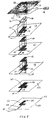
- a metallic sign 50 e.g., a sign.having a metal substrate, having a front surface 52 and a rear surface (not shown in Figure 4) is first positioned in an automated flat bed screen printing press (not shown in Figure 4).
- a rear electrode 54 such as screen printable carbon or silver, having an illumination area 56 and a rear electrode lead 58 is then screen printed onto front surface 52 of sign 50.
- Illumination area 56 defines a light emitting design, or shape, e.g., an "L", representative of the ultimate image to be illuminated on sign 50.
- Rear electrode lead 58 extends from illumination area 56 to a perimeter 60 of sign front surface 52.
- Rear electrode 54 is screen printed as a positive, or forward, image, e.g., as "L " rather than as a reverse “L”. After printing rear electrode 54 on front surface 52, rear electrode 54 is cured to dry. For example, rear electrode 54 and sign 50 may be positioned in a reel to reel oven for approximately two minutes at a temperature of about 176.7°C (350 degrees Fahrenheit).
- dielectric layer 62 is then screen printed onto sign surface 52 so that dielectric layer 62 covers substantially the entire illumination area 56 while leaving rear electrode lead 58 substantially uncovered.
- dielectric layer 62 includes two layers (not shown) of high dielectric constant material, such as barium titanate dispersed in a polymeric binder.
- the first layer of barium titanate is screen printed over rear electrode 54 and then cured to dry for approximately two minutes at a temperature of about 176.7°C (350 degrees Fahrenheit).
- the second layer of barium titanate is then screen printed over the first layer of barium titanate and cured to dry for approximately two minutes at a temperature of about 176.7°C (350 degrees Fahrenheit) to form dielectric layer 62.
- dielectric layer 62 has substantially the same shape as illumination area 56, but is approximately 2% larger than illumination area 56.
- a phosphor layer 64 is screen printed onto sign surface 52 over dielectric layer 62.
- Phosphor layer 64 is screened as a forward, or positive, image, e.g., as "L”, rather than a reverse image, e.g., as a reverse image of "L", and has substantially the same shape and size as illumination area 56.
- Phosphor layer 64 may, for example, be screen printed to sign 50 with the same screen utilized to print rear electrode 54 to sign 50.
- Phosphor layer 64 is then cured, for example, for approximately two minutes at about 350 degrees Fahrenheit.
- Indium tin oxide layer 66 is then screen printed over phosphor layer 64.
- Indium tin oxide layer 66 has substantially the same shape and size as illumination area 56 and may, for example, be screen printed with the same screen utilized to print phosphor layer 64.
- Indium tin oxide layer 66 also is screened as a forward image and is cured, for example, for approximately two minutes at about 176.7°C (350 degrees Fahrenheit).
- a front electrode, or bus bar, 68 fabricated from silver ink is screen printed onto sign surface 52 and configured to transport energy to indium tin oxide layer 66.
- front electrode 68 is screen printed to sign surface 52 so that a first portion 70 of front electrode 68 contacts the outer perimeter of indium tin oxide layer 66, and thus the outer perimeter of illumination area 56, and a front electrode lead 72 extends from illumination area 56 to perimeter 60 of sign surface 52.
- Front electrode 68 is then cured for approximately two minutes at about 176.7°C (350 degrees Fahrenheit).
- Rear electrode 54, dielectric layer 62, phosphor layer 64, indium tin oxide layer 66. and front electrode 68 form an EL lamp extending from surface 52 of sign 50.
- a background layer 74 is then screen printed on front surface 52 of sign 50.
- Background layer 74 substantially covers front surface 52 except for illumination area 56 and a terminal tab portion 76 of front surface 52.
- background layer 74 substantially covers front electrode 68, the portion of dielectric layer 62 not aligned with illumination area 56, and rear electrode 54.
- Terminal tab portion 76 is adjacent sign perimeter 60 and is uncovered to facilitate coupling a power supply 78 to front electrode lead 72 and rear electrode lead 58.
- background layer 74 is screen printed on front surface 52 so that substantially only background layer 74 and indium tin oxide layer 66 are visible from a location facing front surface 52.
- Background layer 74 may include, for example, conventional UV screen printing ink and may be cured in a UV dryer utilizing known sign screening practices.
- Sign 50 may then be embossed so that sign front surface 52 is not planar. Particularly, sign 50 may be embossed so that illumination area 56 projects forward with respect to sign perimeter 60. Alternatively, sign 50 may be embossed so that one portion of illumination area 56, e.g., the short leg of "L", projects forward with respect to another portion or illumination area 56, e.g, the long leg of "L". For example, sign 50 may be positioned in a metal press configured to deliver five tons of pressure per square inch to form dimples in sign front surface 52.
- sign After applying rear electrode 54, dielectric layer 62, phosphor layer 64, indium tin oxide layer 66, front electrode 68, and background layer 74 to sign 50, sign may, for example, be hung in a window, on a wall, or suspended from a ceiling.
- Power supply 78 is then coupled to front electrode lead 72 and rear electrode lead 58 and applies a voltage across rear electrode 54 and front electrode 68 to activate phosphor layer 64. Particularly, current is transmitted through front electrode 68 to indium tin oxide layer 66, and through rear electrode 54 to illumination area 56 to illuminate the letter "L".
- rear electrode 54 is approximately 0.6 millimeters thick
- dielectric layer 62 is approximately 1.2 millimeters thick
- phosphor layer 64 is approximately 1.6 millimeters thick
- indium tin oxide layer 66 is approximately 1.6 millimeters thick
- front bus bar 68 is approximately 0.6 millimeters thick
- background layer 74 is approximately 0.6 millimeters thick.
- each of the various thicknesses may vary.
- the above described method provides an illuminated sign having an EL lamp but does not require coupling a prefabricated EL lamp to the sign. Such method also facilitates applying each layers of the EL lamp to the EL substrate as a positive image, rather than a reverse image.
- an ultraviolet (UV) coating may be applied to sign 50.
- the UV coating may be applied to cover entire front surface 52 of sign 50 and to provide protection to the EL lamp formed by rear electrode 54, dielectric layer 62, phosphor layer 64, indium tin oxide layer 66, and front electrode 68.
- the front surface 52 of sign 50 is coated with a UV curable coating before applying rear electrode 54 to front surface 52.
- a UV coating is first applied to front surface 52 to substantially ensure the integrity of the EL lamp layers, e.g., to substantially prevent the cardboard substrate from absorbing the screen printable inks.
- a sign which includes several EL lamps.
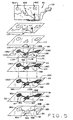
- Figure 5 is an exploded pictorial illustration of a metallic sign 80 having three EL lamps 82A, 82B, and 82C configured as a circle, a triangle, and a square, respectively.
- Sign 80 includes a front surface 84 and a rear surface (not shown in Figure 5) and is first positioned in an automated flat bed screen printing press (not shown in Figure 5).
- a rear electrode 86 such as screen printable carbon or silver, having three illumination areas 88A, 88B, and 88C, and three rear electrode leads 90A, 90B, and 90C is then screen printed onto front surface 84 of sign 80.
- Illumination area 88A defines a light emitting design, or shape, e.g., a circle, representative of the ultimate image to be illuminated by EL lamp 82A on sign 80.
- Illumination area 88B defines a light emitting design, or shape, e.g., a triangle, representative of the ultimate image to be illuminated by EL lamp 82B on sign 80.
- Illumination area 88C defines a light emitting design, or shape, e.g., a square, representative of the ultimate image to be illuminated by EL lamp 82C on sign 80.
- Rear electrode lead 90A extends between illumination area 88A and illumination area 88B.
- Rear electrode lead 90B extends between illumination area 88B and illumination area 88C.
- Rear electrode lead 90C extends from illumination area 88B to a perimeter 92 of sign front surface 84.
- Rear electrode 86 is screen printed as a positive, or forward, image. After printing rear electrode 86 on front surface 84, rear electrode 86 is cured to dry.
- dielectric layer 94 is then screen printed onto sign surface 84 so that dielectric layer 94 substantially covers rear electrode 86 while leaving a portion of rear electrode lead 90 substantially uncovered.
- dielectric layer 94 includes two layers (not shown) of high dielectric constant material, such as barium titanate dispersed in a polymeric binder.
- the first layer of barium titanate is screen printed over rear electrode 86 and then cured to dry for approximately two minutes. at a temperature of about 176.7°C (350 degrees Fahrenheit).
- the second layer of barium titanate is then screen printed over the first layer of barium titanate and cured to dry for approximately two minutes at a temperature of about 176.7°C (350 degrees Fahrenheit) to form dielectric layer 94.
- dielectric layer 94 has three illumination portions 96A, 96B, and 96C which are substantially the same shape as, and approximately 2% larger than, respective illumination areas 88A, 88B, and 88C.
- dielectric layer 94 includes two lead portions 98A and 98B sized to cover rear electrode leads 90A and 90B, respectively.
- a phosphor layer 100 is screen printed onto sign surface 84 over dielectric layer 94.
- Phosphor layer 100 includes three portions 102A, 102B, and 102C, respectively, which are substantially the same shape and size as illumination areas 88A, 88B and 88C, respectively.
- Phosphor layer 100 may, for example, be screen printed to sign 80 with the same screen utilized to print rear electrode 86 to sign 80.
- Phosphor layer 100 is then cured, for. example, for approximately two minutes at about 350 degrees Fahrenheit.
- Indium tin oxide layer 104 is then screen printed over phosphor layer 100.
- Indium tin oxide layer 104 includes three portions 106A, 106B, and 106C, respectively, which have substantially the same shape and size as illumination areas 88A, 88B, and 88C, respectively.
- Indium tin oxide layer 104 may, for example, be screen printed with the same screen utilized to print phosphor layer 100.
- Indium tin oxide layer 104 also is screened as a forward image and is cured, for example, for approximately two minutes at about 350 degrees Fahrenheit.
- a front electrode, or bus bar, 108 fabricated from silver ink is screen printed onto sign surface 84 and configured to transport energy to indium tin oxide layer 104.
- front electrode 108 is screen printed to sign surface 84 so that a first portion 110A of front electrode 108 contacts the outer perimeter of indium tin oxide layer portion 106A, a second portion 110B contacts the outer perimeter of indium tin oxide layer portion 106B, and a third portion 110C contacts the outer perimeter of indium tin oxide layer portion 106C.
- First portion 110A includes a front electrode lead 112A which extends from illumination area 88A to perimeter 92 of sign surface 84.
- second portion 110B includes a front electrode lead 112B which extends from illumination area 88B to perimeter 92 of sign surface 84 and third portion 110C includes a front electrode lead 112C which extends from illumination area 88C to perimeter 92 of sign surface 84.
- Front electrode 108 is then cured for approximately two minutes at about 176.7°C (350 degrees Fahrenheit).
- Rear electrode 86, dielectric layer 94, phosphor layer 100, indium tin oxide layer 104, and front electrode 108 form an EL lamp extending from surface 84 of sign 80.
- a background layer 114 is then screen printed on front surface 84 of sign 80.
- Background layer 114 substantially covers front surface 84 except for illumination area 88 and a terminal tab portion 116 of front surface 84.
- background layer 114 substantially covers front electrode 108, the portion of dielectric layer 94 not aligned with illumination areas 88A, 88B, and 88C, and rear electrode 86.
- Terminal tab portion 116 is adjacent sign perimeter 92 and is uncovered to facilitate coupling a power supply 118 to front electrode lead 112 and rear electrode lead 90.
- background layer 114 is screen printed on front surface 84 so that substantially only background layer 114 and indium tin oxide layer 104 are visible from a location facing front surface 84.
- Background layer 114 may include, for example, conventional UV curable screen printing ink and may be cured in a UV dryer utilizing known sign screening practices.
- background layer 114 may include several conventional US screen printing inks and configured as a design, such as background layer 120.
- Sign 80 may then be embossed so that sign front surface 84 is not planar. Particularly, sign 80 may be embossed so that, for example, illumination area 88A projects forward with respect to illumination area 88B. Alternatively sign 80 may be embossed so that illumination area 88B projects forward with respect to illumination area 88A.
- the above described signs include EL lamps but do not require couple prefabricated EL lamps to the sign. Such signs also are fabricated by screen printing each layer of the EL lamps as a positive image, rather than a reverse image.
- a plastic sign including EL lamps is provided. Particularly, and referring now to Figure 6, a front electrode defining an illumination area eg "L" ( Figure 4), is screen printed 130 to a rear surface of a substantially clear plastic sign. After screen printing 130 the front electrode, an indium tin oxide layer is screen printed 132 to the rear surface, and a phosphor layer is screen printed 134 to the indium tin oxide layer. Subsequently, a dielectric layer is screen printed 136 over the phosphor layer. The front electrode and phosphor layer are configured to define a light emitting design. A rear electrode is then screen printed 138 over the dielectric layer to form an EL lamp. Accordingly, the plastic sign includes an EL lamp without requiring a prefabricated EL lamp to be coupled to the sign.
- a substantially clear heat stabilized polycarbonate sign 140 e.g., a sign having a plastic substrate, having a front surface 142A and a rear surface 142B is first positioned in an automated flat bed screen printing press (not shown in Figure 7).
- a background substrate 144 is screen printed to rear surface 142B and covers substantially entire rear surface 142B except for an illumination area 146 thereof.
- Illumination area 146 is shaped as a reverse image, e.g., a reverse image of "R", of a desired image to be illuminated, e.g., an "R".
- a dielectric background layer 148 is then screen printed over sign rear surface 142B and background substrate 144.
- Dielectric background layer 148 covers substantially entire background substrate 144 and includes an illumination portion 150 which is substantially aligned with illumination area 146.
- a front electrode 152 fabricated from silver ink is then screen printed onto sign rear surface 142B so that front electrode 152 contacts the outer perimeter of illumination portion 150.
- a lead 154 of front electrode 152 extends from the perimeter of illumination portion 150 to a perimeter 156 of sign 140.
- Front electrode 152 is then cured for approximately two minutes at about 176.7°C (350 degrees Fahrenheit).
- an indium tin oxide layer 158 is screen printed onto rear sign surface 142B.
- Indium tin oxide layer 158 is the same size and shape as illumination area 146 and is screen printed as a reverse image, e.g., a reverse image of "R", onto illumination area 146 of rear sign surface 142B.
- Indium tin oxide layer 158 is then cured, for example, for approximately two minutes at about 176.7°C (350 degrees Fahrenheit).
- a phosphor layer 160 is screen printed over indium tin oxide layer 158.
- Phosphor layer 160 is screened as a reverse image and has substantially the same shape and size as indium tin oxide layer 158.
- Phosphor layer 160 may, for example, be screen printed to sign 140 with the same screen utilized to print indium tin oxide layer 158.
- Phosphor layer 160 is then cured, for example, for approximately two minutes at about 176.7°C (350 degrees Fahrenheit).
- dielectric layer 162 is then screen printed onto sign surface 142B so that dielectric layer 162 covers substantially entire phosphor layer 160 and front electrode 152.
- dielectric layer 162 includes two layers (not shown) of high dielectric constant material, such as barium titanate dispersed in a polymeric binder.
- the first layer of barium titanate is screen printed over phosphor layer 160 and then cured to dry for approximately two minutes at a temperature of about 350 degrees Fahrenheit.
- the second layer of barium titanate is then screen printed over the first layer of barium titanate and cured to dry for approximately two minutes at a temperature of about 176.7°C (350 degrees Fahrenheit) to form dielectric layer 162.
- dielectric layer 162 has substantially the same shape as illumination area 146, but is approximately 2% larger than illumination area 146 and is sized to cover at least a portion of front electrode lead 154.
- a rear electrode 164 is screen printed to rear surface 142B over dielectric layer 162 and includes and illumination portion 166 and a rear electrode lead 168. Illumination portion 166 is substantially the same size and shape as illumination area 146, and rear electrode lead 168 extends from illumination portion 166 to sign perimeter 156.
- Rear electrode 164 may be formed from, for example, screen printable carbon.
- Rear electrode 164, dielectric layer 162, phosphor layer 160, indium tin oxide layer 158, and front electrode 152 form an EL lamp extending from rear surface 142B of sign 140.
- a UV curable clear coat (not shown in Figure 7) is screen printed to rear surface 142B and covers rear electrode 164, dielectric layer 162, phosphor layer 160, indium tin oxide layer 158, front electrode 152, dielectric background layer 148 and background layer 144.
- the UV clear coat covers substantially entire rear surface 142B except for a terminal portion 170, through which a portion of front electrode lead 154 and rear electrode lead 168 are exposed to facilitate coupling a power supply (not shown in Figure 7) to such leads 154 and 168.
- Sign may then, for example, be hung in a window, on a wall, or suspended from a ceiling so that illumination area 146 is a positive image, e.g., "R", when viewed from a location adjacent front surface 142A of sign 140.
- illumination area 146 is a positive image, e.g., "R" when viewed from a location adjacent front surface 142A of sign 140.
- flat EL sign 140 may be vacuum formed into a substantially three dimensional shape.
- sign 140 may placed on top of a mandrel form and may then be vacuum formed in accordance with known vacuum forming techniques.
Landscapes
- Physics & Mathematics (AREA)
- General Physics & Mathematics (AREA)
- Engineering & Computer Science (AREA)
- Theoretical Computer Science (AREA)
- Electroluminescent Light Sources (AREA)
- Illuminated Signs And Luminous Advertising (AREA)
Claims (8)
- Verfahren zum Bilden einer integralen elektrolumineszenten Lampe und eines Anzeigeschildes (50), wobei das Anzeigeschild (50) eine Oberfläche (52) aufweist, und das Verfahren die nachfolgenden Schritte umfasst:Bilden einer ultravioletten aushärtbaren Beschichtung an der Oberfläche des Schildes;Bilden einer ersten Elektrode (54) an der Oberfläche des Schildes;Bilden einer Indiumzinnoxidschicht (66) an der Oberfläche des Schildes;Mittels Siebdruck erfolgendes Aufbringen einer Phosphorschicht (64) über der Indiumzinnoxidschicht (66);Mittels Siebdruck erfolgendes Aufbringen einer dielektrischen Schicht (62) auf die Schildoberfläche; undBilden einer zweiten Elektrode (68) an der Schildoberfläche über der dielektrischen Schicht (62).
- Verfahren nach Anspruch 1, bei dem das Schild (50) aus im Wesentlichen klarem Kunststoff hergestellt ist und eine hintere Oberfläche aufweist, und bei dem das Bilden einer ersten Elektrode (54) an der Oberfläche (52) des Schildes den Schritt des mittels Siebdruck erfolgenden Aufbringens einer hinteren Elektrode (54) an der hinteren Oberfläche des Schildes umfasst.
- Verfahren nach Anspruch 2, bei dem das Schild (50) des Weiteren einen Beleuchtungsbereich (56) umfasst, und bei dem das Verfahren des Weiteren den Schritt des mittels Siebdruck erfolgenden Aufbringens einer dielektrischen Hintergrundschicht (74) über der Schildoberfläche umfasst, wobei die dielektrische Hintergrundschicht (74) einen Beleuchtungsabschnitt umfasst, der im Wesentlichen mit dem Beleuchtungsbereich (56) ausgerichtet ist.
- Verfahren nach Anspruch 3, bei dem der Schritt des Bildens einer ersten Elektrode (54) den Schritt des mittels Siebdruck derart erfolgenden Aufbringens einer ersten Elektrode (54) auf die Schildoberfläche umfasst, dass die erste Elektrode (54) den Außenumfang des Beleuchtungsbereiches (56) kontaktiert.
- Verfahren nach Anspruch 1, bei dem der Schritt des Bildens einer Indiumzinnoxidschicht (66) den Schritt des mittels Siebdruck erfolgenden Aufbringens einer Schicht aus Indiumzinnoxid (66) auf die Schildoberfläche (52) umfasst.
- Verfahren nach Anspruch 1, bei dem der Schritt des Bildens einer zweiten Elektrode (68) an der Schildoberfläche über der dielektrischen Schicht (62) den Schritt des mittels Siebdruck erfolgenden Aufbringens einer vorderen Elektrode (68) über der dielektrischen Schicht (62) umfasst.
- Verfahren nach Anspruch 1, des Weiteren umfassend einen anfänglichen Schritt des mittels Druck erfolgenden Aufbringens eines Hintergrundsubstrates auf die Oberfläche (52) des Schildes.
- Schild (50) mit einer Oberfläche (52) und einer damit gekoppelten beleuchteten Ausgestaltung (56), wobei die beleuchtete Ausgestaltung (56) umfasst:eine ultraviolette aushärtbare Beschichtung, die an der Schildoberfläche gebildet ist;eine erste Elektrode (54), die an der Schildoberfläche gebildet ist;eine Indiumzinnoxidschicht (66), die mittels Siebdruck auf der Schildoberfläche aufgebracht ist;eine Phosphorschicht (64), die mittels Siebdruck auf der Indiumzinnoxidschicht (66) aufgebracht ist;eine dielektrische Schicht (62), die mittels Siebdruck auf die Schildoberfläche aufgebracht ist; undeine zweite Elektrode (68), die an der Schildoberfläche über der dielektrischen Schicht (62) gebildet ist.
Applications Claiming Priority (3)
| Application Number | Priority Date | Filing Date | Title |
|---|---|---|---|
| US08/905,528 US6203391B1 (en) | 1997-08-04 | 1997-08-04 | Electroluminescent sign |
| US905528 | 1997-08-04 | ||
| PCT/US1998/016063 WO1999006157A1 (en) | 1997-08-04 | 1998-07-28 | Electroluminescent sign |
Publications (3)
| Publication Number | Publication Date |
|---|---|
| EP1001853A1 EP1001853A1 (de) | 2000-05-24 |
| EP1001853A4 EP1001853A4 (de) | 2001-04-18 |
| EP1001853B1 true EP1001853B1 (de) | 2005-04-06 |
Family
ID=25420990
Family Applications (1)
| Application Number | Title | Priority Date | Filing Date |
|---|---|---|---|
| EP98937320A Expired - Lifetime EP1001853B1 (de) | 1997-08-04 | 1998-07-28 | Elektroluminescentes schild |
Country Status (11)
| Country | Link |
|---|---|
| US (2) | US6203391B1 (de) |
| EP (1) | EP1001853B1 (de) |
| JP (1) | JP2001511596A (de) |
| KR (1) | KR100328305B1 (de) |
| CN (2) | CN1096308C (de) |
| AT (1) | ATE292523T1 (de) |
| AU (1) | AU737834B2 (de) |
| BR (1) | BR9811928A (de) |
| CA (1) | CA2299684C (de) |
| DE (1) | DE69829666T2 (de) |
| WO (1) | WO1999006157A1 (de) |
Families Citing this family (68)
| Publication number | Priority date | Publication date | Assignee | Title |
|---|---|---|---|---|
| US6751898B2 (en) * | 1996-07-23 | 2004-06-22 | George W. Heropoulos | Electroluminescent display apparatus |
| US6965196B2 (en) * | 1997-08-04 | 2005-11-15 | Lumimove, Inc. | Electroluminescent sign |
| TW556357B (en) | 1999-06-28 | 2003-10-01 | Semiconductor Energy Lab | Method of manufacturing an electro-optical device |
| US20010042329A1 (en) * | 2000-04-13 | 2001-11-22 | Matthew Murasko | Electroluminescent sign |
| AU2001257039A1 (en) * | 2000-04-13 | 2001-10-30 | Lumimove, Inc. | Electroluminescent sign |
| WO2002077953A1 (en) * | 2001-03-21 | 2002-10-03 | Lumimove, Inc. | Illuminated display system |
| ATE377257T1 (de) * | 2001-03-22 | 2007-11-15 | Lumimove Inc | Beleuchtetes anzeigesystem und prozess |
| WO2002077518A1 (en) * | 2001-03-22 | 2002-10-03 | Lumimove, Inc. | Integrated illumination system |
| US7048400B2 (en) * | 2001-03-22 | 2006-05-23 | Lumimove, Inc. | Integrated illumination system |
| WO2002077520A1 (en) * | 2001-03-22 | 2002-10-03 | Lumimove, Inc. | Integrated helmet illumination system |
| KR20020076849A (ko) * | 2001-03-30 | 2002-10-11 | 전영국 | 플라스틱 박막형 전계발광소자 및 그 제조방법 |
| US20050007406A1 (en) * | 2001-04-19 | 2005-01-13 | Haas William S. | Controllable thermal warming devices |
| US7022950B2 (en) * | 2001-04-19 | 2006-04-04 | Haas William S | Thermal warming devices |
| US20060001727A1 (en) * | 2001-04-19 | 2006-01-05 | Haas William S | Controllable thermal warming device |
| EP1433155A2 (de) * | 2001-04-30 | 2004-06-30 | Lumimove, Inc. | Elektrolumineszenzbauelemente, die mit verkapselten lichtemittierenden polymerpartikeln hergestellt werden |
| JP2004531867A (ja) * | 2001-06-27 | 2004-10-14 | ルミムーブ, インコーポレイテッド | 制御可能な透明性度を有するエレクトロルミネセンスパネル |
| US6607413B2 (en) * | 2001-06-29 | 2003-08-19 | Novatech Electro-Luminescent, Inc. | Method for manufacturing an electroluminescent lamp |
| EP1415109B1 (de) * | 2001-07-23 | 2005-02-02 | Ledi Lite Ltd | Signalvorrichtung mit interner beleuchtung |
| WO2003012885A1 (en) * | 2001-07-27 | 2003-02-13 | The Ohio State University | Methods for producing electroluminescent devices by screen printing |
| US6541296B1 (en) * | 2001-11-14 | 2003-04-01 | American Trim, Llc | Method of forming electroluminescent circuit |
| US20040007972A1 (en) * | 2002-07-10 | 2004-01-15 | Chih-Yuan Wang | Electro-luminescent device |
| US7361413B2 (en) | 2002-07-29 | 2008-04-22 | Lumimove, Inc. | Electroluminescent device and methods for its production and use |
| US7029763B2 (en) * | 2002-07-29 | 2006-04-18 | Lumimove, Inc. | Light-emitting phosphor particles and electroluminescent devices employing same |
| US20040090789A1 (en) * | 2003-08-21 | 2004-05-13 | Aaron Golle | Snow removal vehicles with colored EL lighting |
| US7128449B2 (en) * | 2003-08-21 | 2006-10-31 | Safe Lites, Llc | Safety device for transporting oversized loads |
| US7306345B2 (en) * | 2002-11-27 | 2007-12-11 | Safe Lites, Llc | High visibility safety sign |
| US20040226601A1 (en) * | 2003-02-24 | 2004-11-18 | Mark Banister | Photovoltaic/solar safety and marker tape |
| DE10308515B4 (de) * | 2003-02-26 | 2007-01-25 | Schott Ag | Verfahren zur Herstellung organischer lichtemittierender Dioden und organische lichtemittierende Diode |
| TWM250833U (en) * | 2003-08-06 | 2004-11-21 | Rilite Corportation | Electroluminescent light band of vehicles |
| GB2404774B (en) * | 2003-08-07 | 2007-02-14 | Pelikon Ltd | Electroluminescent displays |
| US20050035705A1 (en) * | 2003-08-11 | 2005-02-17 | Haas William S. | Illumination system |
| US20040080957A1 (en) * | 2003-08-21 | 2004-04-29 | Aaron Golle | Moduflaps with EL lighting |
| US20040080929A1 (en) * | 2003-08-21 | 2004-04-29 | Aaron Golle | EL safety sign construction |
| US20040080956A1 (en) * | 2003-08-21 | 2004-04-29 | Aaron Golle | Multi-colored EL safety sign |
| US7775540B2 (en) | 2004-02-25 | 2010-08-17 | Scott James Young | Non-rotating bicycle wheel display disk |
| US20050246928A1 (en) * | 2004-04-19 | 2005-11-10 | Joy World, Inc. | Illuminating display |
| US20060072303A1 (en) * | 2004-10-06 | 2006-04-06 | Dunkle Thomas K | Marine warning sign |
| US20060138948A1 (en) * | 2004-12-27 | 2006-06-29 | Quantum Paper, Inc. | Addressable and printable emissive display |
| KR20080014727A (ko) * | 2004-12-27 | 2008-02-14 | 퀀덤 페이퍼, 인크. | 어드레스 가능 및 프린트 가능 발광 디스플레이 |
| US20060138944A1 (en) * | 2004-12-27 | 2006-06-29 | Quantum Paper | Addressable and printable emissive display |
| WO2006084081A2 (en) * | 2005-02-04 | 2006-08-10 | Appleton Coated, Llc | Display with self-illuminatable image and method for making the display substrate and for making the image |
| US7645177B2 (en) | 2005-05-07 | 2010-01-12 | Hewlett-Packard Development Company, L.P. | Electroluminescent panel with inkjet-printed electrode regions |
| GB0514642D0 (en) * | 2005-07-18 | 2005-08-24 | Contra Vision Ltd | Electroluminescent one-way vision panel |
| US7781023B2 (en) * | 2005-10-11 | 2010-08-24 | Hewlett-Packard Development Company, L.P. | Method of producing an electroluminescent display |
| US7582000B2 (en) * | 2006-01-07 | 2009-09-01 | Electro-Luminx Lighting Corporation | Method of making an electroluminescent light |
| US20080141569A1 (en) * | 2006-12-14 | 2008-06-19 | Reyland Mark T | Structure having a wrap and method of wrapping said structure |
| US7972030B2 (en) | 2007-03-05 | 2011-07-05 | Intematix Corporation | Light emitting diode (LED) based lighting systems |
| US7883226B2 (en) * | 2007-03-05 | 2011-02-08 | Intematix Corporation | LED signal lamp |
| US9018833B2 (en) | 2007-05-31 | 2015-04-28 | Nthdegree Technologies Worldwide Inc | Apparatus with light emitting or absorbing diodes |
| US8674593B2 (en) | 2007-05-31 | 2014-03-18 | Nthdegree Technologies Worldwide Inc | Diode for a printable composition |
| US9534772B2 (en) | 2007-05-31 | 2017-01-03 | Nthdegree Technologies Worldwide Inc | Apparatus with light emitting diodes |
| US8415879B2 (en) | 2007-05-31 | 2013-04-09 | Nthdegree Technologies Worldwide Inc | Diode for a printable composition |
| US9419179B2 (en) | 2007-05-31 | 2016-08-16 | Nthdegree Technologies Worldwide Inc | Diode for a printable composition |
| US8852467B2 (en) | 2007-05-31 | 2014-10-07 | Nthdegree Technologies Worldwide Inc | Method of manufacturing a printable composition of a liquid or gel suspension of diodes |
| US8846457B2 (en) | 2007-05-31 | 2014-09-30 | Nthdegree Technologies Worldwide Inc | Printable composition of a liquid or gel suspension of diodes |
| US8877101B2 (en) | 2007-05-31 | 2014-11-04 | Nthdegree Technologies Worldwide Inc | Method of manufacturing a light emitting, power generating or other electronic apparatus |
| US9425357B2 (en) | 2007-05-31 | 2016-08-23 | Nthdegree Technologies Worldwide Inc. | Diode for a printable composition |
| US8384630B2 (en) * | 2007-05-31 | 2013-02-26 | Nthdegree Technologies Worldwide Inc | Light emitting, photovoltaic or other electronic apparatus and system |
| US8889216B2 (en) * | 2007-05-31 | 2014-11-18 | Nthdegree Technologies Worldwide Inc | Method of manufacturing addressable and static electronic displays |
| US8809126B2 (en) | 2007-05-31 | 2014-08-19 | Nthdegree Technologies Worldwide Inc | Printable composition of a liquid or gel suspension of diodes |
| US9343593B2 (en) | 2007-05-31 | 2016-05-17 | Nthdegree Technologies Worldwide Inc | Printable composition of a liquid or gel suspension of diodes |
| US8127477B2 (en) | 2008-05-13 | 2012-03-06 | Nthdegree Technologies Worldwide Inc | Illuminating display systems |
| US7992332B2 (en) * | 2008-05-13 | 2011-08-09 | Nthdegree Technologies Worldwide Inc. | Apparatuses for providing power for illumination of a display object |
| US20090320340A1 (en) * | 2008-06-30 | 2009-12-31 | Panel El Ltd | Illuminated road sign and a method for illuminating a road sign |
| KR20120036940A (ko) * | 2009-06-05 | 2012-04-18 | 코닌클리즈케 필립스 일렉트로닉스 엔.브이. | 전계 발광 장치 |
| US10312731B2 (en) | 2014-04-24 | 2019-06-04 | Westrock Shared Services, Llc | Powered shelf system for inductively powering electrical components of consumer product packages |
| CN109812781B (zh) * | 2017-11-21 | 2021-04-20 | 黄鸣 | 发光玻璃结构及其形成方法 |
| KR102349407B1 (ko) * | 2019-02-01 | 2022-01-11 | 한국전자기술연구원 | 스크린 프린팅 인쇄기술을 이용한 도로 표지판 및 제조방법 |
Family Cites Families (7)
| Publication number | Priority date | Publication date | Assignee | Title |
|---|---|---|---|---|
| US3007007A (en) * | 1958-03-27 | 1961-10-31 | Automatic Elect Lab | Toll ticketing telephone system |
| US3007070A (en) | 1960-02-01 | 1961-10-31 | Controls Co Of America | Electroluminescent device |
| US4904901A (en) * | 1984-12-03 | 1990-02-27 | Lumel, Inc. | Electrolumescent panels |
| US5051654A (en) * | 1988-12-16 | 1991-09-24 | Loctite Luminescent Systems, Inc. | Electroluminescent lamp and method of manufacture |
| US5491377A (en) * | 1993-08-03 | 1996-02-13 | Janusauskas; Albert | Electroluminescent lamp and method |
| US5667417A (en) * | 1995-02-22 | 1997-09-16 | Stevenson; William C. | Method for manufacturing an electroluminescent lamp |
| US5856031A (en) * | 1996-05-30 | 1999-01-05 | E.L. Specialists, Inc. | EL lamp system in kit form |
-
1997
- 1997-08-04 US US08/905,528 patent/US6203391B1/en not_active Expired - Lifetime
-
1998
- 1998-07-28 DE DE69829666T patent/DE69829666T2/de not_active Expired - Lifetime
- 1998-07-28 BR BR9811928-1A patent/BR9811928A/pt not_active Application Discontinuation
- 1998-07-28 EP EP98937320A patent/EP1001853B1/de not_active Expired - Lifetime
- 1998-07-28 CN CN98809568A patent/CN1096308C/zh not_active Expired - Fee Related
- 1998-07-28 AT AT98937320T patent/ATE292523T1/de not_active IP Right Cessation
- 1998-07-28 AU AU86058/98A patent/AU737834B2/en not_active Ceased
- 1998-07-28 KR KR1020007001205A patent/KR100328305B1/ko not_active Expired - Fee Related
- 1998-07-28 WO PCT/US1998/016063 patent/WO1999006157A1/en not_active Ceased
- 1998-07-28 CA CA002299684A patent/CA2299684C/en not_active Expired - Fee Related
- 1998-07-28 JP JP2000504959A patent/JP2001511596A/ja active Pending
-
2000
- 2000-09-21 US US09/666,994 patent/US6424088B1/en not_active Expired - Fee Related
-
2002
- 2002-10-09 CN CN02146928A patent/CN1420481A/zh active Pending
Also Published As
| Publication number | Publication date |
|---|---|
| DE69829666T2 (de) | 2006-03-09 |
| CN1096308C (zh) | 2002-12-18 |
| EP1001853A1 (de) | 2000-05-24 |
| BR9811928A (pt) | 2000-08-22 |
| AU737834B2 (en) | 2001-08-30 |
| KR20010022611A (ko) | 2001-03-26 |
| US6203391B1 (en) | 2001-03-20 |
| CN1271320A (zh) | 2000-10-25 |
| CA2299684A1 (en) | 1999-02-11 |
| US6424088B1 (en) | 2002-07-23 |
| WO1999006157A1 (en) | 1999-02-11 |
| JP2001511596A (ja) | 2001-08-14 |
| CA2299684C (en) | 2008-07-22 |
| CN1420481A (zh) | 2003-05-28 |
| AU8605898A (en) | 1999-02-22 |
| DE69829666D1 (de) | 2005-05-12 |
| EP1001853A4 (de) | 2001-04-18 |
| KR100328305B1 (ko) | 2002-03-16 |
| ATE292523T1 (de) | 2005-04-15 |
Similar Documents
| Publication | Publication Date | Title |
|---|---|---|
| AU737834B2 (en) | Electroluminescent sign | |
| US6965196B2 (en) | Electroluminescent sign | |
| US5583394A (en) | Electroluminescent lamp with registration index feature and method of making the same | |
| CA1105429A (en) | Multi-panel electroluminescent light assembly | |
| US7049536B1 (en) | Electroluminescent lamp membrane switch | |
| US7582000B2 (en) | Method of making an electroluminescent light | |
| US20080079012A1 (en) | Illuminated devices utilizing transparent light active sheet material with integrated light emitting diode (LED), and methods and kit therefor | |
| EP0545558B1 (de) | Anzeigevorrichtung mit elektrolumineszenter Beleuchtung | |
| US20020157173A1 (en) | Integrated helmet illumination system | |
| GB2284699A (en) | Three dimensional electroluminescent display | |
| US20010042329A1 (en) | Electroluminescent sign | |
| US20060291186A1 (en) | Electroluminescent lamp with graphical overlay | |
| MXPA00001316A (en) | Electroluminescent sign | |
| WO2001080272A2 (en) | Electroluminescent sign | |
| KR200395821Y1 (ko) | 광고안내판 | |
| JP2692690B2 (ja) | 電界発光素子 | |
| JP2838777B2 (ja) | El発光装置 | |
| JP2760370B2 (ja) | 分散型電界発光パネル |
Legal Events
| Date | Code | Title | Description |
|---|---|---|---|
| PUAI | Public reference made under article 153(3) epc to a published international application that has entered the european phase |
Free format text: ORIGINAL CODE: 0009012 |
|
| 17P | Request for examination filed |
Effective date: 20000201 |
|
| AK | Designated contracting states |
Kind code of ref document: A1 Designated state(s): AT BE CH CY DE DK ES FI FR GB GR IE IT LI NL PT SE |
|
| A4 | Supplementary search report drawn up and despatched |
Effective date: 20010301 |
|
| AK | Designated contracting states |
Kind code of ref document: A4 Designated state(s): AT BE CH CY DE DK ES FI FR GB GR IE IT LI NL PT SE |
|
| RIC1 | Information provided on ipc code assigned before grant |
Free format text: 7B 05D 5/12 A, 7H 05B 33/10 B, 7H 05B 33/12 B, 7H 05B 33/26 B, 7B 44F 1/10 B, 7G 09F 13/22 B |
|
| 17Q | First examination report despatched |
Effective date: 20021204 |
|
| GRAP | Despatch of communication of intention to grant a patent |
Free format text: ORIGINAL CODE: EPIDOSNIGR1 |
|
| GRAS | Grant fee paid |
Free format text: ORIGINAL CODE: EPIDOSNIGR3 |
|
| GRAA | (expected) grant |
Free format text: ORIGINAL CODE: 0009210 |
|
| AK | Designated contracting states |
Kind code of ref document: B1 Designated state(s): AT BE CH CY DE DK ES FI FR GB GR IE IT LI NL PT SE |
|
| PG25 | Lapsed in a contracting state [announced via postgrant information from national office to epo] |
Ref country code: NL Free format text: LAPSE BECAUSE OF FAILURE TO SUBMIT A TRANSLATION OF THE DESCRIPTION OR TO PAY THE FEE WITHIN THE PRESCRIBED TIME-LIMIT Effective date: 20050406 Ref country code: IT Free format text: LAPSE BECAUSE OF FAILURE TO SUBMIT A TRANSLATION OF THE DESCRIPTION OR TO PAY THE FEE WITHIN THE PRESCRIBED TIME-LIMIT;WARNING: LAPSES OF ITALIAN PATENTS WITH EFFECTIVE DATE BEFORE 2007 MAY HAVE OCCURRED AT ANY TIME BEFORE 2007. THE CORRECT EFFECTIVE DATE MAY BE DIFFERENT FROM THE ONE RECORDED. Effective date: 20050406 Ref country code: FI Free format text: LAPSE BECAUSE OF FAILURE TO SUBMIT A TRANSLATION OF THE DESCRIPTION OR TO PAY THE FEE WITHIN THE PRESCRIBED TIME-LIMIT Effective date: 20050406 Ref country code: AT Free format text: LAPSE BECAUSE OF FAILURE TO SUBMIT A TRANSLATION OF THE DESCRIPTION OR TO PAY THE FEE WITHIN THE PRESCRIBED TIME-LIMIT Effective date: 20050406 |
|
| REG | Reference to a national code |
Ref country code: GB Ref legal event code: FG4D |
|
| REG | Reference to a national code |
Ref country code: CH Ref legal event code: EP |
|
| REG | Reference to a national code |
Ref country code: IE Ref legal event code: FG4D |
|
| REF | Corresponds to: |
Ref document number: 69829666 Country of ref document: DE Date of ref document: 20050512 Kind code of ref document: P |
|
| PG25 | Lapsed in a contracting state [announced via postgrant information from national office to epo] |
Ref country code: SE Free format text: LAPSE BECAUSE OF FAILURE TO SUBMIT A TRANSLATION OF THE DESCRIPTION OR TO PAY THE FEE WITHIN THE PRESCRIBED TIME-LIMIT Effective date: 20050706 Ref country code: GR Free format text: LAPSE BECAUSE OF FAILURE TO SUBMIT A TRANSLATION OF THE DESCRIPTION OR TO PAY THE FEE WITHIN THE PRESCRIBED TIME-LIMIT Effective date: 20050706 Ref country code: DK Free format text: LAPSE BECAUSE OF FAILURE TO SUBMIT A TRANSLATION OF THE DESCRIPTION OR TO PAY THE FEE WITHIN THE PRESCRIBED TIME-LIMIT Effective date: 20050706 |
|
| PG25 | Lapsed in a contracting state [announced via postgrant information from national office to epo] |
Ref country code: ES Free format text: LAPSE BECAUSE OF FAILURE TO SUBMIT A TRANSLATION OF THE DESCRIPTION OR TO PAY THE FEE WITHIN THE PRESCRIBED TIME-LIMIT Effective date: 20050717 |
|
| PG25 | Lapsed in a contracting state [announced via postgrant information from national office to epo] |
Ref country code: IE Free format text: LAPSE BECAUSE OF NON-PAYMENT OF DUE FEES Effective date: 20050728 Ref country code: CY Free format text: LAPSE BECAUSE OF FAILURE TO SUBMIT A TRANSLATION OF THE DESCRIPTION OR TO PAY THE FEE WITHIN THE PRESCRIBED TIME-LIMIT Effective date: 20050728 |
|
| PG25 | Lapsed in a contracting state [announced via postgrant information from national office to epo] |
Ref country code: PT Free format text: LAPSE BECAUSE OF FAILURE TO SUBMIT A TRANSLATION OF THE DESCRIPTION OR TO PAY THE FEE WITHIN THE PRESCRIBED TIME-LIMIT Effective date: 20050908 |
|
| NLV1 | Nl: lapsed or annulled due to failure to fulfill the requirements of art. 29p and 29m of the patents act | ||
| REG | Reference to a national code |
Ref country code: CH Ref legal event code: NV Representative=s name: ISLER & PEDRAZZINI AG |
|
| PLBE | No opposition filed within time limit |
Free format text: ORIGINAL CODE: 0009261 |
|
| STAA | Information on the status of an ep patent application or granted ep patent |
Free format text: STATUS: NO OPPOSITION FILED WITHIN TIME LIMIT |
|
| 26N | No opposition filed |
Effective date: 20060110 |
|
| ET | Fr: translation filed | ||
| REG | Reference to a national code |
Ref country code: IE Ref legal event code: MM4A |
|
| REG | Reference to a national code |
Ref country code: CH Ref legal event code: PCAR Free format text: ISLER & PEDRAZZINI AG;POSTFACH 1772;8027 ZUERICH (CH) |
|
| PGFP | Annual fee paid to national office [announced via postgrant information from national office to epo] |
Ref country code: CH Payment date: 20100726 Year of fee payment: 13 |
|
| PGFP | Annual fee paid to national office [announced via postgrant information from national office to epo] |
Ref country code: GB Payment date: 20100616 Year of fee payment: 13 Ref country code: FR Payment date: 20100813 Year of fee payment: 13 Ref country code: DE Payment date: 20100730 Year of fee payment: 13 |
|
| PGFP | Annual fee paid to national office [announced via postgrant information from national office to epo] |
Ref country code: BE Payment date: 20100714 Year of fee payment: 13 |
|
| BERE | Be: lapsed |
Owner name: *LUMIMOVE CY MO L.L.C. Effective date: 20110731 |
|
| REG | Reference to a national code |
Ref country code: CH Ref legal event code: PL |
|
| GBPC | Gb: european patent ceased through non-payment of renewal fee |
Effective date: 20110728 |
|
| REG | Reference to a national code |
Ref country code: FR Ref legal event code: ST Effective date: 20120330 |
|
| PG25 | Lapsed in a contracting state [announced via postgrant information from national office to epo] |
Ref country code: BE Free format text: LAPSE BECAUSE OF NON-PAYMENT OF DUE FEES Effective date: 20110731 Ref country code: CH Free format text: LAPSE BECAUSE OF NON-PAYMENT OF DUE FEES Effective date: 20110731 Ref country code: FR Free format text: LAPSE BECAUSE OF NON-PAYMENT OF DUE FEES Effective date: 20110801 Ref country code: LI Free format text: LAPSE BECAUSE OF NON-PAYMENT OF DUE FEES Effective date: 20110731 Ref country code: DE Free format text: LAPSE BECAUSE OF NON-PAYMENT OF DUE FEES Effective date: 20120201 |
|
| REG | Reference to a national code |
Ref country code: DE Ref legal event code: R119 Ref document number: 69829666 Country of ref document: DE Effective date: 20120201 |
|
| PG25 | Lapsed in a contracting state [announced via postgrant information from national office to epo] |
Ref country code: GB Free format text: LAPSE BECAUSE OF NON-PAYMENT OF DUE FEES Effective date: 20110728 |