EP0998699B1 - Electronic protection circuit - Google Patents
Electronic protection circuit Download PDFInfo
- Publication number
- EP0998699B1 EP0998699B1 EP98940175A EP98940175A EP0998699B1 EP 0998699 B1 EP0998699 B1 EP 0998699B1 EP 98940175 A EP98940175 A EP 98940175A EP 98940175 A EP98940175 A EP 98940175A EP 0998699 B1 EP0998699 B1 EP 0998699B1
- Authority
- EP
- European Patent Office
- Prior art keywords
- capacitor
- comparator
- signal
- output
- reset
- Prior art date
- Legal status (The legal status is an assumption and is not a legal conclusion. Google has not performed a legal analysis and makes no representation as to the accuracy of the status listed.)
- Expired - Lifetime
Links
Images


Classifications
-
- G—PHYSICS
- G06—COMPUTING; CALCULATING OR COUNTING
- G06F—ELECTRIC DIGITAL DATA PROCESSING
- G06F1/00—Details not covered by groups G06F3/00 - G06F13/00 and G06F21/00
- G06F1/24—Resetting means
-
- G—PHYSICS
- G05—CONTROLLING; REGULATING
- G05B—CONTROL OR REGULATING SYSTEMS IN GENERAL; FUNCTIONAL ELEMENTS OF SUCH SYSTEMS; MONITORING OR TESTING ARRANGEMENTS FOR SUCH SYSTEMS OR ELEMENTS
- G05B9/00—Safety arrangements
- G05B9/02—Safety arrangements electric
Abstract
Description
Die vorliegende Erfindung bezieht sich auf eine elektronische Sicherheitsschaltung nach
dem Gattungsbegriff des Patentanspruches 1. Eine derartige Sicherheitsschaltung ist aus
US-A-4,727,549 oder US-A-4,879,647 bekannt. Hinsichtlich weiteren Standes der Technik
wird auf US-A-5,508,910 und JP-A-57055432 verwiesen.The present invention relates to an electronic safety circuit according to
the generic term of
Bei Steuerungen mit sicherheitskritischen Anwendungen werden heutzutage Mikrokontroller eingesetzt, um programmgesteuert irgendwelche Stellglieder zu betätigen. Wenn der Mikrokontroller nicht ordnungsgemäß arbeitet, weil z.B. sein Taktgenerator ausfällt, so muß sichergestellt werden, daß die gesamte Steuerung in einen Zustand gebracht wird, in welchem die Stellglieder nach der sicheren Seite betätigt werden. Beispielsweise darf ein Brennstoffventil in einem solchen Fall nicht geöffnet werden.Controls with safety-critical applications are used today Microcontroller used to operate any actuators under program control. If the microcontroller is not working properly, e.g. because his clock generator fails, it must be ensured that the entire control system is in one state is brought in which the actuators are operated on the safe side. For example, a fuel valve must not be opened in such a case.
Die ordnungsgemäße Funktion eines Mikrokontrollers kann beispielsweise überwacht werden, indem man programmgesteuert periodisch ein Start/Rücksetzsignal an einem seiner Ausgänge erzeugt, dessen Auftritt überwacht wird. Beim Ausbleiben dieses Signales wird ein Reset-Signal erzeugt, durch das der Mikrokontroller stillgesetzt wird. Hiervon ausgehend ist es die Aufgabe der vorliegenden Erfindung, eine elektronische Sicherheitsschaltung anzugeben, die die Betätigung eines Stellgliedes nur ermöglicht, wenn ein in die Steuerung einbezogener Mikrokontroller ordnungsgemäß arbeitet.The proper functioning of a microcontroller can be monitored, for example be made by periodically programming a start / reset signal on a of its outputs, whose occurrence is monitored. If there is no signal a reset signal is generated, which shuts down the microcontroller. Proceeding from this, the object of the present invention is an electronic Specify a safety circuit that only enables the actuation of an actuator when a microcontroller included in the controller is working properly.
Die Lösung dieser Aufgabe gelingt gemäß den kennzeichnenden Merkmalen des
Patentanspruches 1. Weitere vorteilhafte Ausgestaltungen der erfindungsgemäßen
Sicherheitsschaltung sind den abhängigen Ansprüchen entnehmbar.This problem is solved in accordance with the characteristic features of
Anhand der Figuren der beiliegenden Zeichnung sei im folgenden ein Ausführungsbeispiel der erfindungsgemäßen Sicherheitsschaltung beschrieben. Es zeigen:
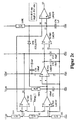
- Fig. 1
- ein Blockschaltbild des grundsätzlichen Aufbaues der Sicherheitsschaltung;
- Fig. 2
- ein detailliertes Schaltungsschema der erfindungsgemäßen Sicherheitsschaltung;
- Fig. 2a
- das Prinzipschaltbild eines Mikrokontrollers;
- Fig. 2b
- die Schaltung eines Rampengenerators;
- Fig. 2c
- das Schaltbild einer Überwachungsschaltung mit eingebauter Verzögerung;
- Fig. 2d
- das Schaltbild eines Reset-Generators; und
- Fig. 2e
- das Schaltbild einer Ventilansteuerung.
- Fig. 1
- a block diagram of the basic structure of the safety circuit;
- Fig. 2
- a detailed circuit diagram of the safety circuit according to the invention;
- Fig. 2a
- the schematic diagram of a microcontroller;
- Fig. 2b
- the circuit of a ramp generator;
- Fig. 2c
- the circuit diagram of a monitoring circuit with built-in delay;
- Fig. 2d
- the circuit diagram of a reset generator; and
- Fig. 2e
- the circuit diagram of a valve control.
Gemäß Fig. 1 liefert eine Steuerung µc ein Ansteuersignal V1 an eine Ansteuereinheit V, die ein zusätzliches Freigabesignal En benötigt, um beim Vorliegen des Ansteuersignales V1 betätigt zu werden. Die Steuerung µc gibt periodisch in einem bestimmten zeitlichen Abstand ein Start- und ein Rücksetzsignal aus, das einem Rampengenerator RG zugeführt wird. Der Hochlauf der Rampe wird durch das Startsignal ausgelöst und durch das Rücksetzsignal beendet, mit welchem gleichzeitig die Rampe zurückgesetzt wird. Start- und Rücksetzsignal bestehen hierbei aus der negativen und positiven Flanke eines Impulses. Eine Auswerteschaltung EV überwacht, ob die Rampe innerhalb einer bestimmten Zeit einen unteren Pegelwert erreicht bzw. einen oberen Pegelwert nicht überschreitet. Wird der untere Pegelwert nicht erreicht oder der obere Pegelwert überschritten. so wird ein Reset für die Steuerung µc erzeugt und ein Freigabesignal für die Ansteuereinheit V gesperrt. Ein Verzögerungsglied DL erzeugt verzögert die Aufhebung der Sperrung des Freigabesignales En an die Ansteuereinheit V. Das Freigabesignal wird solange gesperrt bis entweder erneut ein Reset erzeugt wurde oder die Steuerung wieder ordnungsgemäß arbeitet. Dadurch wird erreicht, daß bei nicht ordnungsgemäßer Funktion der Steuerung µc die Ansteuereinheit V permanent gesperrt wird.According to FIG. 1, a control μc supplies a control signal V1 to a control unit V, which requires an additional enable signal En to be present when the control signal is present V1 to be operated. The control µc gives periodically in a certain time Distance a start and a reset signal, which is fed to a ramp generator RG becomes. The ramp-up is triggered by the start signal and by the Reset signal ended, with which the ramp is reset at the same time. Begin- and reset signal consist of the negative and positive edge of one Impulse. An evaluation circuit EV monitors whether the ramp is within a reaches a lower level value for a certain time or does not reach an upper level value exceeds. If the lower level value is not reached or the upper level value exceeded. so a reset for the control µc is generated and an enable signal for the Control unit V blocked. A delay element DL delays the cancellation blocking the enable signal En to the control unit V. The enable signal is blocked until either a reset has been generated again or the control again works properly. This ensures that if it does not function properly the control unit Vc the control unit V is permanently blocked.
Gemäß Fig. 2 umfaßt die elektronische Sicherheitsschaltung die Steuerung µc, den Rampengenerator RG. die Auswertung und Verzögerung EV, DL, den Reset-Generator Res und die Ansteuereinheit V. In den Figuren 2a bis 2e ist jedes dieser Schaltungselemente vergrößert dargestellt, wobei Aufbau und Funktion der erfindungsgemäßen Sicherheitsschaltung anhand dieser Figuren beschrieben wird.2, the electronic safety circuit includes the control µc, the RG generator ramp. the evaluation and delay EV, DL, the reset generator Res and the control unit V. In FIGS. 2a to 2e each of these circuit elements shown enlarged, the structure and function of the safety circuit according to the invention is described with reference to these figures.
Gemäß Fig. 2, 2a besteht die Steuerung aus einem handelsüblichen Mikrokontroller µc, der mit einem Quarzresonator beschaltet ist. Der Mikrokontroller wird zwischen der Betriebsspannung ULog (VDD = 5V) und Masse (Gnd) betrieben und er weist eine Reihe von Aus- und Eingängen auf, von denen für die Funktion der vorliegenden Erfindung nur die folgenden von Bedeutung sind:
- /Res
- Reseteingang, der bei hohem Potential (z.B.
grösser kleiner - RRes
- Ausgang, der durch Programmierung des Mikrokontrollers bei dessen ordnungsgemäßer Funktion das Start/Rücksetz-Signal periodisch ausgibt; und
- V1
- Ausgang, der der Betätigung eines Stellgliedes dient, z.B. eines Brennstoffventiles in einer sicherheitsrelevanten Anwendung bei einem Feuerungsautomaten.
- / Res
- Reset input that enables the function of the microcontroller at high potential (eg greater than 0.8 ULog) and prevents it at low potential (less than 0.2 ULog);
- RRes
- Output that periodically outputs the start / reset signal by programming the microcontroller when it is functioning properly; and
- V1
- Output that serves to actuate an actuator, eg a fuel valve in a safety-relevant application in an automatic burner control.
Gemäß Fig. 2. 2b wird der Ausgang RRes auf einen Rampengenerator bekannter Bauart geschaltet. Der Rampengenerator besteht aus einem Kondensator C84, der über einen Widerstand R84 aus der Betriebsspannung ULog aufgeladen wird, wobei die Zeitkonstante durch die RC-Kombination vorgegeben wird. Der gemeinsame Verbindungspunkt von Widerstand und Kondensator liefert die Rampenspannung und ist über einen relativ niedrigen Widerstand R86 und einen Transistor T86 mit dem Bezugspotential Gnd verbindbar. Die Basis des Transistors T86 liegt über einen Widerstand R83 an der Betriebsspannung ULog und wird zusätzlich von dem Signal RRes beaufschlagt. Ist dieser Ausgang hochohmig (Open), so ist der Transistor T86 im stromführenden Zustand und der Kondensator C84 wird über den relativ niederohmigen Widerstand R86 rasch entladen. Ist der Ausgangspegel tief, so wird der Transistor T86 gesperrt und die Rampe läuft hoch, da der Kondensator C84 über den Widerstand R84 aufgeladen wird.According to Fig. 2. 2b, the output RRes on a ramp generator of a known type switched. The ramp generator consists of a capacitor C84, which is connected via a Resistor R84 is charged from the operating voltage ULog, the time constant is determined by the RC combination. The common connection point of Resistor and capacitor provides the ramp voltage and is relative across one low resistance R86 and a transistor T86 with the reference potential Gnd connectable. The base of transistor T86 is connected to the resistor R83 Operating voltage ULog and is additionally acted upon by the signal RRes. Is this Output high resistance (Open), the transistor T86 is in the current-carrying state and the Capacitor C84 is rapidly discharged through the relatively low resistance R86. Is the output level low, the transistor T86 is blocked and the ramp runs up because capacitor C84 is charged through resistor R84.
Gemäß Fig. 2. 2c wird das Ausgangssignal des Rampengenerators auf eine Überwachungs- und Verzögerungsschaltung geschaltet. Diese umfaßt an ihrem Eingang einen Spannungsteiler. bestehend aus der Reihenschaltung dreier Widerstände R71, R72, R73, die zwischen Betriebsspannung ULog und Bezugspotential Gnd geschaltet sind. Hierdurch werden an den Abgriffpunkten des Spannungsteilers Schwellwertspannungen von ca. 3,2V und 4.2V vorgegeben. Diese Abgriffpunkte sind auf die Pluseingänge von zwei Komparatoren IC70B und IC70C geführt, deren Minuseingängen das Rampensignal zugeführt wird. Der Ausgang des die untere Schwelle (3,2V) überwachenden Komparators IC70B ist über einen Kondensator C71 an Bezugspotential gelegt, während der Ausgang des die obere Schwelle (4,2V) überwachenden Komparators IC70C über einen Kondensator C73 an Bezugspotential gelegt ist. Ferner ist der Kondensator C71 über einen Widerstand R74 an die Betriebsspannung ULog angeschlossen. Der Kondensator C73 liegt über die Reihenschaltung zweier Widerstände R94, R93 an der Betriebsspannung. Der gemeinsame Schaltungspunkt von Kondensator C71 und Widerstand R74 ist an den Minuseingang eines weiteren Komparators IC70A angeschlossen, dessen Pluseingang ebenfalls mit dem unteren Schwellwert (3,2V) verbunden ist. Der Ausgang des Komparators IC70A liegt ebenfalls an dem Kondensator C73 und ist ferner über einen Kondensator C72 mit dem unteren Schwellwert (3,2V) verbunden. Der Ausgang des Komparators IC 70A liegt am Pluseingang eines weiteren Komparators IC70D. dessen Minuseingang an dem unteren Schwellwert (3,2V) liegt. Der Ausgang des Komparators IC70D liegt über einen Kondensator C76 an Bezugspotential und ferner über einen Widerstand R75 am Kollektor eines Transistors T97, der über einen Widerstand R97 ebenfalls an Bezugspotential liegt. Eine Diode D76 liegt zwischen Ausgängen der Komparatoren IC70B und IC70D und damit auch zwischen den beiden Kondensatoren C71 und C76.According to FIG. 2c, the output signal of the ramp generator is applied to a monitoring and delay circuit switched. This includes one at its entrance Voltage divider. consisting of the series connection of three resistors R71, R72, R73, which are connected between the operating voltage ULog and the reference potential Gnd. Hereby threshold voltages of approx.3.2V at the tapping points of the voltage divider and 4.2V specified. These taps are on the plus inputs of two Comparators IC70B and IC70C led, the negative inputs of the ramp signal is fed. The output of the comparator monitoring the lower threshold (3.2V) IC70B is connected to reference potential through a capacitor C71 while the output of the comparator IC70C monitoring the upper threshold (4.2V) via a Capacitor C73 is connected to reference potential. Furthermore, the capacitor C71 is via a Resistor R74 connected to the operating voltage ULog. The capacitor C73 lies via the series connection of two resistors R94, R93 at the operating voltage. The common node of capacitor C71 and resistor R74 is at the Minus input of another comparator IC70A connected, its plus input is also connected to the lower threshold (3.2V). The exit of the Comparator IC70A is also connected to the capacitor C73 and is also via a Capacitor C72 connected to the lower threshold (3.2V). The exit of the Comparator IC 70A is located at the plus input of another comparator IC70D. whose Minus input is at the lower threshold (3.2V). The output of the comparator IC70D is connected to reference potential via a capacitor C76 and also via a Resistor R75 on the collector of a transistor T97, which is connected via a resistor R97 is also due to reference potential. A diode D76 lies between the outputs of the Comparators IC70B and IC70D and thus also between the two capacitors C71 and C76.
Der Ausgang des Komparators IC70D und somit auch der Kondensator C76 sind an den Pluseingang eines weiteren Komparators IC10D angeschlossen, dessen Minuseingang an dem oberen Schwellwert (4,2V) liegt. Am Ausgang des Komparators IC10D wird das Verriegelungssignal VR abgenommen.The output of the comparator IC70D and thus also the capacitor C76 are connected to the Plus input of another comparator IC10D connected, whose minus input to the upper threshold (4.2V). At the output of the comparator IC10D this is Lock signal VR removed.
Alle Komparatoren dieser Überwachungsschaltung werden zwischen einer Spannung URel von etwa 22V und Bezugspotential betrieben. Jeder Komparator ist an seinem Ausgang hochohmig. wenn der Pluseingang über dem Minuseingang liegt und er weist umgekehrt einen tiefen Pegel auf. wenn der Minuseingang über dem Pluseingang liegt.All comparators of this monitoring circuit are between a voltage URel operated by about 22V and reference potential. Each comparator is at its exit high impedance. if the plus input is above the minus input and it points the other way round a low level. if the negative input is above the positive input.
Gemäß Fig. 2. 2d umfaßt ein Reset-Generator einen ersten Transistor T94. dessen Emitter an der Betriebsspannung liegt und dessen Basis an den gemeinsamen Schaltungspunkt der Widerstände R93. R94 angeschlossen ist. Der Kollektor des Transistors T94 ist an die Basis eines weiteren Transistors T97 angeschlossen, dessen Emitter ebenfalls mit der Betriebsspannung verbunden ist und dessen Kollektor wie bereits erwähnt über den Widerstand R97 an das Bezugspotential gelegt ist. Ein Spannungsteiler, bestehend aus den Widerständen R95, R96 ist zwischen die Betriebsspannung ULog und Bezugspotential Gnd geschaltet und hält den Transistor T97 normalerweise im stromführenden Zustand, so daß das am Kollektor des Transistors T97 abgenommene Reset-Signal /Res ein hohes Potential geringfügig unter der Betriebsspannung aufweist.According to FIG. 2. 2d, a reset generator comprises a first transistor T94. its emitter is due to the operating voltage and its base at the common node of the Resistors R93. R94 is connected. The collector of transistor T94 is connected to the Base of another transistor T97 connected, whose emitter also with the Operating voltage is connected and its collector as already mentioned on the Resistor R97 is connected to the reference potential. A voltage divider consisting of the Resistors R95, R96 is between the operating voltage ULog and reference potential Gnd is switched and holds the transistor T97 normally in the live state, so that the reset signal / Res on the collector of transistor T97 has a high potential slightly below the operating voltage.
Nur wenn der Kondensator C73 entladen und wieder aufgeladen wird und ein Strom über die Widerstände R93, R94 fließt, gelangt der Transistor T94 in den stromführenden Zustand und der Transistor T97 wird gesperrt, so daß ein Reset-Signal /Res mit niedrigem Pegel erzeugt wird. Dieses Reset-Signal bringt den Mikrokontroller in einen definierten Zustand, bei dem das Ansteuersignal V1 nicht erzeugt wird.Only when capacitor C73 is discharged and recharged and does a current flow through the resistors R93, R94 flows, the transistor T94 gets into the current-carrying State and transistor T97 is turned off, causing a reset signal / Res to be low Level is generated. This reset signal brings the microcontroller into a defined one State in which the control signal V1 is not generated.
Gemäß Fig. 2, 2e ist ein Transistor T78 angeordnet, dessen Emitter an Bezugspotential liegt und dessen Kollektor über eine Relaisspule RV1A des Ventils V an die Betriebsspannung URel angeschlossen ist. Die Basis des Transistors T78 wird über die Reihenschaltung zweier Widerstände R76, R78 mit dem Ansteuersignal V1 des Mikrokontrollers angesteuert. Der gemeinsame Schaltungspunkt der beiden Widerstände R76, R78 liegt über einen Kondensator C78 an Bezugspotential und das Verriegelungssignal VR liegt ebenfalls an diesem gemeinsamen Schaltungspunkt, so daß eine Betätigung des Transistors T78 verhindert wird. solange das Verriegelungssignal VR den niedrigen Pegel aufweist. Dies ist der Fall, solange ein Reset erzeugt wird (C73 ist entladen bzw. wird aufgeladen; C76 ist teilweise entladen und muß mit entsprechend großer Zeitkonstante wieder nachgeladen werden). Die beiden Zenerdioden Z76, Z77 am Eingang der Schaltung dienen der Spannungsbegrenzung und dem Schutz der Schaltung.2, 2e, a transistor T78 is arranged, the emitter of which is at reference potential lies and the collector via a relay coil RV1A of valve V to the Operating voltage URel is connected. The base of transistor T78 is over the Series connection of two resistors R76, R78 with the control signal V1 des Microcontroller controlled. The common circuit point of the two resistors R76, R78 is connected to reference potential via a capacitor C78 and that Lock signal VR is also at this common node, so that actuation of the transistor T78 is prevented. as long as the locking signal VR has the low level. This is the case as long as a reset is generated (C73 is unloading or charging; C76 is partially discharged and must be used accordingly large time constant can be reloaded). The two Zener diodes Z76, Z77 am Input of the circuit serve to limit the voltage and protect the circuit.
Anhand des vorstehend beschriebenen Aufbaues sei im folgenden die Funktion der erfindungsgemäßen Sicherheitsschaltung näher erläutert.Based on the structure described above, the function of safety circuit according to the invention explained in more detail.
Grundsätzlich wird ein Reset für den Mikrokontroller erzeugt durch Entladung und Wiederaufladung des Kondensators C73. Dies geschieht, wenn die Rampe den unteren Schwellwert (3,2V) nicht oder verspätet erreicht. In diesem Fall bleibt der Ausgang des Komparators IC70B permanent oder zu lange hochohmig, so daß der Kondensator C71 über den Widerstand R74 auf 3,2V oder höher aufgeladen wird. Dann schaltet aber der Komparator IC70A an seinem Ausgang auf den tiefen Pegel und entlädt den Kondensator C73. Basically, a reset for the microcontroller is generated by discharging and Recharge the C73 capacitor. This happens when the ramp hits the bottom Threshold value (3.2V) not reached or delayed. In this case, the exit of the Comparator IC70B permanent or too long high resistance, so that the capacitor C71 is charged to 3.2V or higher via resistor R74. Then the switches Comparator IC70A at its output to the low level and discharges the capacitor C73.
Gleiches geschieht, wenn die Rampe den oberen Schwellwert (4,2V) überschreitet. Dann schaltet der Ausgang des Komparators IC70C auf den tiefen Pegel und entlädt den Kondensator C73.The same happens if the ramp exceeds the upper threshold (4.2V). Then the output of the comparator IC70C switches to the low level and discharges the Capacitor C73.
Bei einer Entladung des Kondensators C73 schaltet auch der Ausgang des Komparators IC70D auf den tiefen Pegel, wodurch der Kondensator C76 entladen wird. Wenn das Potential des Kondensators C76 unter 4,2V fällt, so gibt der Komparator IC10D den tiefen Pegel aus. mit welchem das Verriegelungssignal VR die Betätigung des Ventils V sperrt. Die Erzeugung des Verriegelungssignales VR ist gleichbedeutend mit einer Sperrung des Freigabesignales En. Die Verriegelung des Ventils kann erst aufgehoben werden, wenn der Kondensator C76 mit relativ großer Zeitkonstante wieder aufgeladen ist, was nur der Fall ist. wenn kein erneuter Reset erfolgt.If the capacitor C73 is discharged, the output of the comparator also switches IC70D to the low level, thereby discharging the capacitor C76. If that Potential of the capacitor C76 falls below 4.2V, the comparator IC10D gives the low one Level off. with which the locking signal VR blocks the actuation of the valve V. The generation of the locking signal VR is synonymous with blocking the Release signal En. The valve can only be unlocked when the Capacitor C76 is recharged with a relatively large time constant, which is only the case is. if there is no renewed reset.
Im Detail ist die Funktion der Schaltung wie folgt:In detail, the function of the circuit is as follows:
Wie bereits erwähnt. schaltet der Ausgang des Komparators IC70A auf den niedrigen Pegel und entlädt den Kondensators C73, wenn der Kondensator C71 auf den unteren Schwellwert von 3,2V aufgeladen wurde oder diesen Schwellwert überschreitet. Über den Kondensator C72 wird eine Hysterese eingeführt, indem der untere Schwellwert kurzfristig auf ein Potential von ca. 3,2 - 5 = -1,8V gezogen wird. Der untere Schwellwert steigt anschließend mit einer Zeitkonstanten von ca. 30µs zurück auf 3.2V. Somit liegt die Rampenspannung zumindest zeitweilig über dem unteren Schwellwert, so daß der Komparator IC70B am Ausgang auf den tiefen Pegel schaltet und den Kondensator C71 entlädt. Je nachdem wie hoch die Rampenspannung ist, wird der Kondensator C71 nur wenig oder vollständig entladen. Die Entladezeit des Kondensators C73 beträgt lediglich 0,1 bis 1.2 µs. so daß dieser vollständig entladen wird, weil der untere Schwellwert während dieser Zeit noch nicht wieder das positive Potential erreicht hat. Wenn der untere Schwellwert das Potential auf dem Kondensator C71 erreicht hat. wird der Kondensator C73 wieder aufgeladen mit einer Zeitkonstanten von ca. 0,8 bis 1,2 ms. Solange der Kondensator C73 entladen ist und wieder geladen wird, fließt ein Strom durch den Transistor T94 und den Widerstand R94 und es wird während ca. 1 bis 5 ms ein Reset erzeugt. Das Potential des Kondensators C73 bleibt während mindestens 0,8 ms unterhalb des unteren Schwellwertes und der Komparator IC70D schaltet solange tief und entlädt den Kondensator C76. Die Entladezeit des Kondensators C76 liegt unterhalb 1 ms. Der Kondensator C76 wird hierbei auf weniger als 0,5V entladen, wodurch über die Diode D76 auch der Kondensator C71 auf etwa 0,5 bis 1V entladen wird. Anschließend werden die Kondensatoren C71 und C76 mit einer Zeitkonstanten von 100 bis 150 ms wieder aufgeladen. Nach erfolgter Aufladung des Kondensators C71 auf 3,2V kann der Zyklus von neuem beginnen. In der Zwischenzeit kann der Mikrokontroller seinen Betrieb starten und die Rampenspannung korrekt erzeugen. Die Aufladung des Kondensators C76 von 3,2V auf 4,2V erfolgt mit einer relativ hohen Zeitkonstanten von 180 bis 300 ms nach dem Reset, während welcher Zeit durch den Komparator IC10D das Verriegelungssignal VR mit tiefem Pegel ausgegeben wird. Der Reset wird erzeugt, wenn die Rampe über eine gewisse Zeit den Schwellwert nicht erreicht. C71 wird periodisch wieder entladen, wenn die Rampe korrekt ist.As already mentioned. the output of the comparator IC70A switches to the low level and discharges capacitor C73 when capacitor C71 drops to the bottom Threshold of 3.2V has been charged or exceeds this threshold. On the Capacitor C72 introduces hysteresis by briefly lowering the lower threshold to a potential of approx. 3.2 - 5 = -1.8V. The lower threshold increases then with a time constant of approx. 30µs back to 3.2V. Thus lies the Ramp voltage at least temporarily above the lower threshold, so that the Comparator IC70B at the output switches to low level and capacitor C71 discharges. Depending on how high the ramp voltage is, the capacitor C71 only discharged little or completely. The discharge time of the capacitor C73 is only 0.1 to 1.2 µs. so that it is completely discharged because of the lower threshold has not yet returned to positive potential during this time. If the lower one Threshold has reached the potential on capacitor C71. becomes the capacitor C73 recharged with a time constant of approx. 0.8 to 1.2 ms. As long as the Capacitor C73 is discharged and recharged, a current flows through it Transistor T94 and resistor R94 and there is a reset for about 1 to 5 ms generated. The potential of the capacitor C73 remains below for at least 0.8 ms of the lower threshold and the comparator IC70D switches low and discharges the Capacitor C76. The discharge time of the capacitor C76 is less than 1 ms. The Capacitor C76 is discharged to less than 0.5 V, causing the diode D76 capacitor C71 is also discharged to about 0.5 to 1V. Then the Capacitors C71 and C76 with a time constant of 100 to 150 ms again charged. After capacitor C71 has been charged to 3.2V, the cycle of start again. In the meantime, the microcontroller can start operating generate the ramp voltage correctly. The charging of the capacitor C76 of 3.2V to 4.2V takes place with a relatively high time constant of 180 to 300 ms after the Reset the time during which the locking signal VR is output at a low level. The reset is generated when the ramp has a certain time does not reach the threshold. C71 is periodically unloaded when the ramp is correct.
Wenn die Rampenspannung den oberen Schwellwert von 4,2V übersteigt, so schaltet der Komparator IC70C an seinem Ausgang auf den niedrigen Pegel und entlädt den Kondensator C73. In der Folge fließt ein Strom durch den Transistor T94 und den Widerstand R94 und der Reset des Mikrokontrollers wird erzeugt. Hierdurch gibt der Mikrokontroller das Signal RRes hochohmig aus, wodurch die Rampenspannung sofort zurückgesetzt wird und der Komparator IC70C am Ausgang wieder den hohen Pegel ausgibt. Die Rampenspannung bleibt solange auf dem tiefen Pegel, bis der Mikrokontroller sie kontrolliert startet. Der Kondensator C73 wird über den Widerstand R94 wieder aufgeladen, wobei die Zeitkonstante bei 0,8 bis 1,2 ms liegt. Solange das Potential auf dem Kondensator C73 unterhalb 3,2V liegt, schaltet der Komparator IC70D auf den tiefen Pegel und entlädt den Kondensator C76. Damit wird wieder über die Diode D76 auch der Kondensator C71 bis ca. 0.5 bis 1V entladen. Dies verzögert das Ansprechen auf den tiefen Rampenwert mindestens für die folgenden 80 ms. Wie bei der Überwachung des unteren Schwellwertes hat der Mikrokontroller solange Zeit zum Neustart. Sofort nach Übersteigen des oberen Schwellwertes durch die Rampenspannung wird die Rampenspannung auf Grund des Resets zurückgesetzt. Damit der Kondensator C73 trotzdem genügend entladen wird, ist auch hier eine dynamische Hysterese über den Kondensator C72 verwirklicht, der den oberen Schwellwert über den Widerstand R72 kurzzeitig absenkt. Würde der Kondensator C73 nicht genügend entladen, so bliebe dem Komparator IC70D nicht genügend Zeit. um den Kondensator C76 zu entladen. Damit bliebe das Potential auf den Kondensatoren C76 und 71 zu hoch und das Ansprechen auf den unteren Schwellwert würde nicht verzögert.If the ramp voltage exceeds the upper threshold of 4.2V, the Comparator IC70C at its output to the low level and discharges the Capacitor C73. As a result, a current flows through transistor T94 and Resistor R94 and the reset of the microcontroller are generated. This gives the Microcontroller the signal RRes high impedance, causing the ramp voltage immediately is reset and the comparator IC70C at the output returns to the high level issues. The ramp voltage remains at the low level until the microcontroller it starts in a controlled manner. The capacitor C73 is turned on through the resistor R94 charged, the time constant being 0.8 to 1.2 ms. As long as the potential on the If the capacitor C73 is below 3.2V, the comparator IC70D switches to the low level and discharges the capacitor C76. This means that the diode D76 is also used Discharge capacitor C71 to approx. 0.5 to 1V. This delays the response to the deep Ramp value for at least the following 80 ms. As with monitoring the bottom The microcontroller has threshold values for as long as to restart. Immediately after exceeding of the upper threshold value by the ramp voltage, the ramp voltage is raised Reset reason of the reset. So that the capacitor C73 discharges enough dynamic hysteresis is also implemented here via the capacitor C72, which briefly lowers the upper threshold via resistor R72. Would the If the capacitor C73 is not sufficiently discharged, the comparator IC70D would not remain enough time. to discharge the capacitor C76. This would leave the potential on Capacitors C76 and 71 too high and the response to the lower threshold wouldn't be delayed.
Der Kondensator C76 speichert den Zustand des Verriegelungssignales RV1. Solange sein Potential unterhalb 4,2V liegt, schaltet der Komparator IC10D an seinem Ausgang auf den tiefen Pegel und schaltet somit den Transistor T78 aus, wodurch das Ventil ausgeschaltet wird. Die Diode D76 sorgt für die Verzögerung nach einem Reset. Bei Entladung des Kondensators C76 wird über die Diode D76 ebenfalls der Kondensator C71 entladen und entsprechend langsam aufgeladen mit einer Zeitkonstanten von etwa 100 bis 150 ms. Der Sperrstrom über die Diode D76 ist so gering, daß über den Widerstand R75 das Reset-Signal nicht wesentlich beeinflußt wird. Der nächste Reset wird jedoch erst verzögert, wenn das Potential des Kondensators C71 kleiner als 3,2V ist. Dann ist auch das Potential des Kondensators C76 kleiner als 3,2V. Die Aufladung des Kondensators C76 von 3,2 auf 4,2V dauert etwa 250 bis 400 ms. Während dieser Zeit bleibt das Verriegelungssignal VR für das Ventil nach der Aufhebung des Resets noch auf dem niedrigen Pegel, wodurch verhindert wird. daß der Mikrokontroller das Ventil einschalten kann bevor die Sicherheitsschaltung eventuell erneut anspricht. Dies führt im Fehlerfall zur permanenten Verriegelung.The capacitor C76 stores the state of the latch signal RV1. As long as Potential is below 4.2V, the comparator IC10D switches to the output low level and thus turns off transistor T78, causing the valve to turn off becomes. The diode D76 provides the delay after a reset. When the Capacitor C76 is also discharged via the diode D76 and the capacitor C71 accordingly charged slowly with a time constant of about 100 to 150 ms. The Reverse current via the diode D76 is so low that the reset signal via the resistor R75 is not significantly affected. The next reset is only delayed, when the potential of capacitor C71 is less than 3.2V. Then there is also the potential of the capacitor C76 less than 3.2V. The charge on the capacitor C76 from 3.2 4.2V takes about 250 to 400 ms. The locking signal VR remains during this time for the valve is still at the low level after the reset is canceled, whereby is prevented. that the microcontroller can turn on the valve before the Safety circuit may respond again. In the event of an error, this leads to permanent Interlock.
Claims (8)
- Electronic protective circuit for a controller (µc) driving a control element (V) with a drive signal (V1), which controller cyclically outputs a start/reset signal at a prescribed time interval during correct operation, having:
a circuit (RG, EV) which monitors the time at which the start/reset signal appears and blocks an enable signal (En) for the control element (V) if the start signal does not appear or if the reset signal does not appear or is late, the block on the enable signal for the control element being cleared with a delay, and the circuit which monitors the time at which the start/reset signal appears additionally generating a blocking signal (Res) and sending it to the controller (µc), the circuit which monitors the time at which the start/reset signal appears comprising a ramp generator (RG) whose ramp is started by the start signal and is reset by the reset signal, characterized in that the circuit which monitors the time at which the start/reset signal appears comprises a level monitoring circuit (EV) with a delay element (DL), and the delay time of the delay element is greater than the period of the ramp function. - Protective circuit according to Claim 1,
characterized in that the level monitoring circuit has:
a first comparator (IC70B), which compares the ramp function with a lower threshold value, a second comparator (IC70C), which compares the ramp function with an upper threshold value, in that the output of the first comparator (IC70B) is connected to a first capacitor (C71), one end of which is connected to operating voltage (ULog) via a resistor (R74), and the other end of which is connected to reference-ground potential (Gnd), in that the output of the second comparator (IC70C) is connected to a second capacitor (C73), one end of which is connected to a reset generator, and the other end of which is connected to reference-ground potential (Gnd), and in that the first capacitor (C71) is connected to a third comparator (IC70A), whose other input likewise has the lower threshold value supplied to it and whose output is connected to the second capacitor (C73). - Protective circuit according to Claim 2,
characterized in that a fourth comparator (IC70D) is provided which compares the charge in the second capacitor (C73) with the lower threshold value and whose output is connected to a third capacitor (C76), one end of which is connected to the output of the reset generator via a resistor (R75), and the other end of which is connected to reference-ground potential (Gnd). - Protective circuit according to Claim 3,
characterized in that the first capacitor (C71) is connected to the third capacitor (C76) via a forward-biased diode (D76). - Protective circuit according to Claim 4,
characterized in that the output of the third capacitor (IC70A) is connected to the lower threshold value via a fourth capacitor (C72). - Protective circuit according to Claim 5,
characterized in that a fifth comparator (IC10D) is provided which compares the output of the fourth comparator (IC70D) with one threshold value and whose output generates the enable signal for the control element. - Protective circuit according to Claim 6,
characterized in that the second capacitor (C73) is connected to the operating voltage (ULog) via the series circuit comprising two resistors (R93, R94), in that the common connection point between the two resistors (R93, R94) is connected to the base of a transistor (T94) whose emitter is connected to the operating voltage (ULog) and whose collector is connected to the base of a further transistor (T97), whose emitter is connected to the operating voltage (ULog) and whose collector is connected to reference-ground potential (Gnd) via a resistor (R97) and generates the reset signal (/Res), the base of the further transistor (T97) being connected to a voltage divider (R95, R96) arranged between operating voltage and reference-ground potential. - Protective circuit according to Calim 7,
characterized in that the drive signal (V1) is connected via two series-connected resistors (R76, R78) to the base of a transistor (T78) whose collector circuit contains a relay coil (RV1A), and in that the common connection point between the two resistors (R76, R78) is connected to reference-ground potential (Gnd) via a capacitor (C78) and is connected to the output of the fifth comparator (IC10D).
Applications Claiming Priority (3)
| Application Number | Priority Date | Filing Date | Title |
|---|---|---|---|
| DE19731086 | 1997-07-19 | ||
| DE19731086A DE19731086C2 (en) | 1997-07-19 | 1997-07-19 | Electronic safety circuit |
| PCT/EP1998/004230 WO1999004324A1 (en) | 1997-07-19 | 1998-07-08 | Electronic protection circuit |
Publications (2)
| Publication Number | Publication Date |
|---|---|
| EP0998699A1 EP0998699A1 (en) | 2000-05-10 |
| EP0998699B1 true EP0998699B1 (en) | 2001-10-24 |
Family
ID=7836273
Family Applications (1)
| Application Number | Title | Priority Date | Filing Date |
|---|---|---|---|
| EP98940175A Expired - Lifetime EP0998699B1 (en) | 1997-07-19 | 1998-07-08 | Electronic protection circuit |
Country Status (7)
| Country | Link |
|---|---|
| EP (1) | EP0998699B1 (en) |
| AT (1) | ATE207628T1 (en) |
| DE (2) | DE19731086C2 (en) |
| DK (1) | DK0998699T3 (en) |
| ES (1) | ES2165184T3 (en) |
| HU (1) | HU2410U (en) |
| WO (1) | WO1999004324A1 (en) |
Families Citing this family (1)
| Publication number | Priority date | Publication date | Assignee | Title |
|---|---|---|---|---|
| DE102015117977A1 (en) | 2015-10-22 | 2017-04-27 | Knorr-Bremse Systeme für Nutzfahrzeuge GmbH | Circuitry and method for monitoring a microcontroller based on a guard voltage |
Family Cites Families (9)
| Publication number | Priority date | Publication date | Assignee | Title |
|---|---|---|---|---|
| JPS5755432A (en) * | 1980-09-20 | 1982-04-02 | Sumitomo Electric Ind Ltd | Watchdog timer circuit |
| DE3322242A1 (en) * | 1982-07-23 | 1984-01-26 | Robert Bosch Gmbh, 7000 Stuttgart | DEVICE FOR FUNCTION MONITORING OF ELECTRONIC DEVICES, IN PARTICULAR MICROPROCESSORS |
| DE3243760C2 (en) * | 1982-11-26 | 1989-04-27 | Brown, Boveri & Cie Ag, 6800 Mannheim | Device for function monitoring of a processor |
| US4879647A (en) * | 1985-06-11 | 1989-11-07 | Nec Corporation | Watchdog timer circuit suited for use in microcomputer |
| US4727549A (en) * | 1985-09-13 | 1988-02-23 | United Technologies Corporation | Watchdog activity monitor (WAM) for use wth high coverage processor self-test |
| DE3604734A1 (en) * | 1986-02-14 | 1987-08-20 | Siemens Ag | Circuit to monitor the progress of a program in a microprocessor |
| DE3639065C2 (en) * | 1986-11-14 | 1997-01-09 | Bosch Gmbh Robert | Process for monitoring a computer-controlled actuating process computer |
| DE3914003C2 (en) * | 1989-04-27 | 1995-10-05 | Siemens Ag | Arrangement for monitoring the program flow of a control module containing at least one microprocessor |
| US5508910A (en) * | 1994-09-26 | 1996-04-16 | Forney International, Inc. | Redundant analog I/O board system |
-
1997
- 1997-07-19 DE DE19731086A patent/DE19731086C2/en not_active Expired - Lifetime
-
1998
- 1998-07-08 HU HU19980000022U patent/HU2410U/en unknown
- 1998-07-08 DE DE59801884T patent/DE59801884D1/en not_active Expired - Lifetime
- 1998-07-08 ES ES98940175T patent/ES2165184T3/en not_active Expired - Lifetime
- 1998-07-08 WO PCT/EP1998/004230 patent/WO1999004324A1/en active IP Right Grant
- 1998-07-08 DK DK98940175T patent/DK0998699T3/en active
- 1998-07-08 AT AT98940175T patent/ATE207628T1/en active
- 1998-07-08 EP EP98940175A patent/EP0998699B1/en not_active Expired - Lifetime
Also Published As
| Publication number | Publication date |
|---|---|
| ES2165184T3 (en) | 2002-03-01 |
| DK0998699T3 (en) | 2002-01-07 |
| DE19731086A1 (en) | 1999-01-28 |
| ATE207628T1 (en) | 2001-11-15 |
| EP0998699A1 (en) | 2000-05-10 |
| DE19731086C2 (en) | 2001-09-13 |
| HU0000022V0 (en) | 2001-07-30 |
| HU2410U (en) | 2002-11-28 |
| DE59801884D1 (en) | 2001-11-29 |
| WO1999004324A1 (en) | 1999-01-28 |
Similar Documents
| Publication | Publication Date | Title |
|---|---|---|
| DE102010043882B4 (en) | Clocked safety switch | |
| DE3421584A1 (en) | RESET CIRCUIT FOR MICROPROCESSORS | |
| DE4230913C2 (en) | Method and circuit arrangement for a serial bus system with a single-wire connection | |
| DE10359225A1 (en) | Driver circuit for a semiconductor device | |
| EP0179194A1 (en) | Device for protecting an electronic anti-skid system against overvoltage | |
| DE3926178A1 (en) | WAKE-UP CIRCUIT FOR A MICROPROCESSOR | |
| DE3322074A1 (en) | EMERGENCY DEVICE FOR MICROCOMPUTER CONTROLLED SYSTEMS | |
| DE3322242A1 (en) | DEVICE FOR FUNCTION MONITORING OF ELECTRONIC DEVICES, IN PARTICULAR MICROPROCESSORS | |
| DE19616851B4 (en) | Protection device to avoid unwanted power supply | |
| EP0482015B1 (en) | Safety system for vehicle occupants | |
| WO1987004758A1 (en) | Device for resetting computer equipment | |
| DE2316433A1 (en) | PROGRAMMABLE UNIVERSAL LOGIC MODULE | |
| EP0998699B1 (en) | Electronic protection circuit | |
| DE3214006A1 (en) | DEVICE FOR RESETTING CALCULATIONS | |
| EP0505774B1 (en) | Security switching device | |
| DE2903638C2 (en) | ||
| DE19811269C1 (en) | Electronic circuit with protective circuit for lubrication controllers in motor vehicles, esp. lorries | |
| EP1480239B1 (en) | Method for operating and monitoring circuit for an electronic-mechanical position switch | |
| DE19843621A1 (en) | Discharge circuit for a capacitive actuator | |
| DE3130307C2 (en) | ||
| EP0794094A2 (en) | Releasing circuit in particular for a safety critical occupant protection system for vehicles transporting people | |
| DE19532677B4 (en) | Monitoring circuit for at least one supply voltage | |
| EP0023695B1 (en) | Surveillance circuitry for an input voltage | |
| DE4132392C2 (en) | Sensor device for a rail contact | |
| WO1991010108A1 (en) | Electronic real-time time fuse |
Legal Events
| Date | Code | Title | Description |
|---|---|---|---|
| PUAI | Public reference made under article 153(3) epc to a published international application that has entered the european phase |
Free format text: ORIGINAL CODE: 0009012 |
|
| 17P | Request for examination filed |
Effective date: 19991113 |
|
| AK | Designated contracting states |
Kind code of ref document: A1 Designated state(s): AT BE CH DE DK ES FI FR GB GR IE IT LI LU MC NL PT SE |
|
| GRAG | Despatch of communication of intention to grant |
Free format text: ORIGINAL CODE: EPIDOS AGRA |
|
| GRAG | Despatch of communication of intention to grant |
Free format text: ORIGINAL CODE: EPIDOS AGRA |
|
| GRAH | Despatch of communication of intention to grant a patent |
Free format text: ORIGINAL CODE: EPIDOS IGRA |
|
| 17Q | First examination report despatched |
Effective date: 20001127 |
|
| GRAH | Despatch of communication of intention to grant a patent |
Free format text: ORIGINAL CODE: EPIDOS IGRA |
|
| GRAA | (expected) grant |
Free format text: ORIGINAL CODE: 0009210 |
|
| AK | Designated contracting states |
Kind code of ref document: B1 Designated state(s): AT BE CH DE DK ES FI FR GB GR IE IT LI LU MC NL PT SE |
|
| PG25 | Lapsed in a contracting state [announced via postgrant information from national office to epo] |
Ref country code: IE Free format text: LAPSE BECAUSE OF FAILURE TO SUBMIT A TRANSLATION OF THE DESCRIPTION OR TO PAY THE FEE WITHIN THE PRESCRIBED TIME-LIMIT Effective date: 20011024 |
|
| REF | Corresponds to: |
Ref document number: 207628 Country of ref document: AT Date of ref document: 20011115 Kind code of ref document: T |
|
| REG | Reference to a national code |
Ref country code: CH Ref legal event code: EP |
|
| REG | Reference to a national code |
Ref country code: IE Ref legal event code: FG4D Free format text: GERMAN |
|
| REF | Corresponds to: |
Ref document number: 59801884 Country of ref document: DE Date of ref document: 20011129 |
|
| REG | Reference to a national code |
Ref country code: GB Ref legal event code: IF02 |
|
| REG | Reference to a national code |
Ref country code: DK Ref legal event code: T3 |
|
| PG25 | Lapsed in a contracting state [announced via postgrant information from national office to epo] |
Ref country code: PT Free format text: LAPSE BECAUSE OF FAILURE TO SUBMIT A TRANSLATION OF THE DESCRIPTION OR TO PAY THE FEE WITHIN THE PRESCRIBED TIME-LIMIT Effective date: 20020124 |
|
| PG25 | Lapsed in a contracting state [announced via postgrant information from national office to epo] |
Ref country code: GR Free format text: LAPSE BECAUSE OF FAILURE TO SUBMIT A TRANSLATION OF THE DESCRIPTION OR TO PAY THE FEE WITHIN THE PRESCRIBED TIME-LIMIT Effective date: 20020125 |
|
| GBT | Gb: translation of ep patent filed (gb section 77(6)(a)/1977) |
Effective date: 20020105 |
|
| ET | Fr: translation filed | ||
| REG | Reference to a national code |
Ref country code: ES Ref legal event code: FG2A Ref document number: 2165184 Country of ref document: ES Kind code of ref document: T3 |
|
| REG | Reference to a national code |
Ref country code: IE Ref legal event code: FD4D |
|
| PGFP | Annual fee paid to national office [announced via postgrant information from national office to epo] |
Ref country code: MC Payment date: 20020702 Year of fee payment: 5 |
|
| PLBE | No opposition filed within time limit |
Free format text: ORIGINAL CODE: 0009261 |
|
| STAA | Information on the status of an ep patent application or granted ep patent |
Free format text: STATUS: NO OPPOSITION FILED WITHIN TIME LIMIT |
|
| PGFP | Annual fee paid to national office [announced via postgrant information from national office to epo] |
Ref country code: LU Payment date: 20020918 Year of fee payment: 5 |
|
| 26N | No opposition filed | ||
| PG25 | Lapsed in a contracting state [announced via postgrant information from national office to epo] |
Ref country code: LU Free format text: LAPSE BECAUSE OF NON-PAYMENT OF DUE FEES Effective date: 20030708 |
|
| PG25 | Lapsed in a contracting state [announced via postgrant information from national office to epo] |
Ref country code: MC Free format text: LAPSE BECAUSE OF NON-PAYMENT OF DUE FEES Effective date: 20030731 |
|
| REG | Reference to a national code |
Ref country code: CH Ref legal event code: PUE Owner name: HONEYWELL TECHNOLOGIES SARL Free format text: SATRONIC AG#HONEYWELL-PLATZ 1#8157 DIELSDORF (CH) -TRANSFER TO- HONEYWELL TECHNOLOGIES SARL#AVENUE DE LA GOTTAZ 34-36#1110 MORGES (CH) Ref country code: CH Ref legal event code: NV Representative=s name: ISLER & PEDRAZZINI AG |
|
| REG | Reference to a national code |
Ref country code: GB Ref legal event code: 732E |
|
| NLS | Nl: assignments of ep-patents |
Owner name: HONEYWELL TECHNOLOGIES SARL Effective date: 20071119 |
|
| REG | Reference to a national code |
Ref country code: FR Ref legal event code: TP |
|
| PGFP | Annual fee paid to national office [announced via postgrant information from national office to epo] |
Ref country code: DK Payment date: 20120626 Year of fee payment: 15 |
|
| PGFP | Annual fee paid to national office [announced via postgrant information from national office to epo] |
Ref country code: FI Payment date: 20120702 Year of fee payment: 15 |
|
| PGFP | Annual fee paid to national office [announced via postgrant information from national office to epo] |
Ref country code: ES Payment date: 20120723 Year of fee payment: 15 Ref country code: BE Payment date: 20120724 Year of fee payment: 15 |
|
| PGFP | Annual fee paid to national office [announced via postgrant information from national office to epo] |
Ref country code: AT Payment date: 20120626 Year of fee payment: 15 |
|
| PGFP | Annual fee paid to national office [announced via postgrant information from national office to epo] |
Ref country code: GB Payment date: 20130624 Year of fee payment: 16 |
|
| PGFP | Annual fee paid to national office [announced via postgrant information from national office to epo] |
Ref country code: CH Payment date: 20130806 Year of fee payment: 16 Ref country code: SE Payment date: 20130708 Year of fee payment: 16 Ref country code: NL Payment date: 20130711 Year of fee payment: 16 Ref country code: DE Payment date: 20130731 Year of fee payment: 16 |
|
| BERE | Be: lapsed |
Owner name: HONEYWELL TECHNOLOGIES SARL Effective date: 20130731 |
|
| REG | Reference to a national code |
Ref country code: DK Ref legal event code: EBP Effective date: 20130731 |
|
| REG | Reference to a national code |
Ref country code: AT Ref legal event code: MM01 Ref document number: 207628 Country of ref document: AT Kind code of ref document: T Effective date: 20130708 |
|
| PG25 | Lapsed in a contracting state [announced via postgrant information from national office to epo] |
Ref country code: BE Free format text: LAPSE BECAUSE OF NON-PAYMENT OF DUE FEES Effective date: 20130731 Ref country code: FI Free format text: LAPSE BECAUSE OF NON-PAYMENT OF DUE FEES Effective date: 20130708 |
|
| PG25 | Lapsed in a contracting state [announced via postgrant information from national office to epo] |
Ref country code: AT Free format text: LAPSE BECAUSE OF NON-PAYMENT OF DUE FEES Effective date: 20130708 |
|
| REG | Reference to a national code |
Ref country code: ES Ref legal event code: FD2A Effective date: 20140807 |
|
| PG25 | Lapsed in a contracting state [announced via postgrant information from national office to epo] |
Ref country code: DK Free format text: LAPSE BECAUSE OF NON-PAYMENT OF DUE FEES Effective date: 20130731 |
|
| PG25 | Lapsed in a contracting state [announced via postgrant information from national office to epo] |
Ref country code: ES Free format text: LAPSE BECAUSE OF NON-PAYMENT OF DUE FEES Effective date: 20130709 |
|
| REG | Reference to a national code |
Ref country code: DE Ref legal event code: R119 Ref document number: 59801884 Country of ref document: DE |
|
| REG | Reference to a national code |
Ref country code: NL Ref legal event code: V1 Effective date: 20150201 |
|
| REG | Reference to a national code |
Ref country code: CH Ref legal event code: PL |
|
| REG | Reference to a national code |
Ref country code: SE Ref legal event code: EUG |
|
| GBPC | Gb: european patent ceased through non-payment of renewal fee |
Effective date: 20140708 |
|
| PG25 | Lapsed in a contracting state [announced via postgrant information from national office to epo] |
Ref country code: NL Free format text: LAPSE BECAUSE OF NON-PAYMENT OF DUE FEES Effective date: 20150201 |
|
| PG25 | Lapsed in a contracting state [announced via postgrant information from national office to epo] |
Ref country code: CH Free format text: LAPSE BECAUSE OF NON-PAYMENT OF DUE FEES Effective date: 20140731 Ref country code: DE Free format text: LAPSE BECAUSE OF NON-PAYMENT OF DUE FEES Effective date: 20150203 Ref country code: LI Free format text: LAPSE BECAUSE OF NON-PAYMENT OF DUE FEES Effective date: 20140731 |
|
| REG | Reference to a national code |
Ref country code: DE Ref legal event code: R119 Ref document number: 59801884 Country of ref document: DE Effective date: 20150203 |
|
| PG25 | Lapsed in a contracting state [announced via postgrant information from national office to epo] |
Ref country code: SE Free format text: LAPSE BECAUSE OF NON-PAYMENT OF DUE FEES Effective date: 20140709 Ref country code: GB Free format text: LAPSE BECAUSE OF NON-PAYMENT OF DUE FEES Effective date: 20140708 |
|
| REG | Reference to a national code |
Ref country code: FR Ref legal event code: PLFP Year of fee payment: 18 |
|
| REG | Reference to a national code |
Ref country code: FR Ref legal event code: PLFP Year of fee payment: 19 |
|
| REG | Reference to a national code |
Ref country code: FR Ref legal event code: PLFP Year of fee payment: 20 |
|
| PGFP | Annual fee paid to national office [announced via postgrant information from national office to epo] |
Ref country code: FR Payment date: 20170727 Year of fee payment: 20 Ref country code: IT Payment date: 20170720 Year of fee payment: 20 |