EP0998699B1 - Elektronische sicherheitsschaltung - Google Patents
Elektronische sicherheitsschaltung Download PDFInfo
- Publication number
- EP0998699B1 EP0998699B1 EP98940175A EP98940175A EP0998699B1 EP 0998699 B1 EP0998699 B1 EP 0998699B1 EP 98940175 A EP98940175 A EP 98940175A EP 98940175 A EP98940175 A EP 98940175A EP 0998699 B1 EP0998699 B1 EP 0998699B1
- Authority
- EP
- European Patent Office
- Prior art keywords
- capacitor
- comparator
- signal
- output
- reset
- Prior art date
- Legal status (The legal status is an assumption and is not a legal conclusion. Google has not performed a legal analysis and makes no representation as to the accuracy of the status listed.)
- Expired - Lifetime
Links
Images


Classifications
-
- G—PHYSICS
- G06—COMPUTING OR CALCULATING; COUNTING
- G06F—ELECTRIC DIGITAL DATA PROCESSING
- G06F1/00—Details not covered by groups G06F3/00 - G06F13/00 and G06F21/00
- G06F1/24—Resetting means
-
- G—PHYSICS
- G05—CONTROLLING; REGULATING
- G05B—CONTROL OR REGULATING SYSTEMS IN GENERAL; FUNCTIONAL ELEMENTS OF SUCH SYSTEMS; MONITORING OR TESTING ARRANGEMENTS FOR SUCH SYSTEMS OR ELEMENTS
- G05B9/00—Safety arrangements
- G05B9/02—Safety arrangements electric
Definitions
- the present invention relates to an electronic safety circuit according to the generic term of claim 1.
- a safety circuit is from US-A-4,727,549 or US-A-4,879,647.
- Controls with safety-critical applications are used today Microcontroller used to operate any actuators under program control. If the microcontroller is not working properly, e.g. because his clock generator fails, it must be ensured that the entire control system is in one state is brought in which the actuators are operated on the safe side. For example, a fuel valve must not be opened in such a case.
- the object of the present invention is an electronic Specify a safety circuit that only enables the actuation of an actuator when a microcontroller included in the controller is working properly.
- a control ⁇ c supplies a control signal V1 to a control unit V, which requires an additional enable signal En to be present when the control signal is present V1 to be operated.
- the control ⁇ c gives periodically in a certain time Distance a start and a reset signal, which is fed to a ramp generator RG becomes.
- the ramp-up is triggered by the start signal and by the Reset signal ended, with which the ramp is reset at the same time.
- Begin- and reset signal consist of the negative and positive edge of one Impulse.
- An evaluation circuit EV monitors whether the ramp is within a reaches a lower level value for a certain time or does not reach an upper level value exceeds. If the lower level value is not reached or the upper level value exceeded.
- a delay element DL delays the cancellation blocking the enable signal En to the control unit V.
- the enable signal is blocked until either a reset has been generated again or the control again works properly. This ensures that if it does not function properly the control unit Vc the control unit V is permanently blocked.
- the electronic safety circuit includes the control ⁇ c, the RG generator ramp. the evaluation and delay EV, DL, the reset generator Res and the control unit V.
- the control ⁇ c the RG generator ramp.
- the evaluation and delay EV the evaluation and delay EV
- DL the reset generator Res
- the control unit V the control unit V.
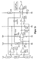
- the ramp generator consists of a capacitor C84, which is connected via a Resistor R84 is charged from the operating voltage ULog, the time constant is determined by the RC combination.
- the common connection point of Resistor and capacitor provides the ramp voltage and is relative across one low resistance R86 and a transistor T86 with the reference potential Gnd connectable.
- the base of transistor T86 is connected to the resistor R83 Operating voltage ULog and is additionally acted upon by the signal RRes. Is this Output high resistance (Open), the transistor T86 is in the current-carrying state and the Capacitor C84 is rapidly discharged through the relatively low resistance R86. Is the output level low, the transistor T86 is blocked and the ramp runs up because capacitor C84 is charged through resistor R84.
- the output signal of the ramp generator is applied to a monitoring and delay circuit switched.
- This includes one at its entrance Voltage divider. consisting of the series connection of three resistors R71, R72, R73, which are connected between the operating voltage ULog and the reference potential Gnd.
- threshold voltages of approx.3.2V at the tapping points of the voltage divider and 4.2V specified. These taps are on the plus inputs of two Comparators IC70B and IC70C led, the negative inputs of the ramp signal is fed.
- the output of the comparator monitoring the lower threshold (3.2V) IC70B is connected to reference potential through a capacitor C71 while the output of the comparator IC70C monitoring the upper threshold (4.2V) via a Capacitor C73 is connected to reference potential. Furthermore, the capacitor C71 is via a Resistor R74 connected to the operating voltage ULog. The capacitor C73 lies via the series connection of two resistors R94, R93 at the operating voltage. The common node of capacitor C71 and resistor R74 is at the Minus input of another comparator IC70A connected, its plus input is also connected to the lower threshold (3.2V). The exit of the Comparator IC70A is also connected to the capacitor C73 and is also via a Capacitor C72 connected to the lower threshold (3.2V).
- the exit of the Comparator IC 70A is located at the plus input of another comparator IC70D. whose Minus input is at the lower threshold (3.2V).
- the output of the comparator IC70D is connected to reference potential via a capacitor C76 and also via a Resistor R75 on the collector of a transistor T97, which is connected via a resistor R97 is also due to reference potential.
- a diode D76 lies between the outputs of the Comparators IC70B and IC70D and thus also between the two capacitors C71 and C76.
- the output of the comparator IC70D and thus also the capacitor C76 are connected to the Plus input of another comparator IC10D connected, whose minus input to the upper threshold (4.2V). At the output of the comparator IC10D this is Lock signal VR removed.
- All comparators of this monitoring circuit are between a voltage URel operated by about 22V and reference potential. Each comparator is at its exit high impedance. if the plus input is above the minus input and it points the other way round a low level. if the negative input is above the positive input.
- a reset generator comprises a first transistor T94. its emitter is due to the operating voltage and its base at the common node of the Resistors R93. R94 is connected. The collector of transistor T94 is connected to the Base of another transistor T97 connected, whose emitter also with the Operating voltage is connected and its collector as already mentioned on the Resistor R97 is connected to the reference potential.
- a voltage divider consisting of the Resistors R95, R96 is between the operating voltage ULog and reference potential Gnd is switched and holds the transistor T97 normally in the live state, so that the reset signal / Res on the collector of transistor T97 has a high potential slightly below the operating voltage.
- a transistor T78 is arranged, the emitter of which is at reference potential lies and the collector via a relay coil RV1A of valve V to the Operating voltage URel is connected.
- the base of transistor T78 is over the Series connection of two resistors R76, R78 with the control signal V1 des Microcontroller controlled.
- the common circuit point of the two resistors R76, R78 is connected to reference potential via a capacitor C78 and that Lock signal VR is also at this common node, so that actuation of the transistor T78 is prevented. as long as the locking signal VR has the low level. This is the case as long as a reset is generated (C73 is unloading or charging; C76 is partially discharged and must be used accordingly large time constant can be reloaded).
- the two Zener diodes Z76, Z77 am Input of the circuit serve to limit the voltage and protect the circuit.
- a reset for the microcontroller is generated by discharging and Recharge the C73 capacitor. This happens when the ramp hits the bottom Threshold value (3.2V) not reached or delayed. In this case, the exit of the Comparator IC70B permanent or too long high resistance, so that the capacitor C71 is charged to 3.2V or higher via resistor R74. Then the switches Comparator IC70A at its output to the low level and discharges the capacitor C73.
- the output of the comparator also switches IC70D to the low level, thereby discharging the capacitor C76. If that Potential of the capacitor C76 falls below 4.2V, the comparator IC10D gives the low one Level off. with which the locking signal VR blocks the actuation of the valve V.
- the generation of the locking signal VR is synonymous with blocking the Release signal En.
- the valve can only be unlocked when the Capacitor C76 is recharged with a relatively large time constant, which is only the case is. if there is no renewed reset.
- the output of the comparator IC70A switches to the low level and discharges capacitor C73 when capacitor C71 drops to the bottom Threshold of 3.2V has been charged or exceeds this threshold.
- the lower threshold increases then with a time constant of approx. 30 ⁇ s back to 3.2V.
- the Ramp voltage at least temporarily above the lower threshold, so that the Comparator IC70B at the output switches to low level and capacitor C71 discharges. Depending on how high the ramp voltage is, the capacitor C71 only discharged little or completely.
- the discharge time of the capacitor C73 is only 0.1 to 1.2 ⁇ s. so that it is completely discharged because of the lower threshold has not yet returned to positive potential during this time. If the lower one Threshold has reached the potential on capacitor C71. becomes the capacitor C73 recharged with a time constant of approx. 0.8 to 1.2 ms. As long as the Capacitor C73 is discharged and recharged, a current flows through it Transistor T94 and resistor R94 and there is a reset for about 1 to 5 ms generated. The potential of the capacitor C73 remains below for at least 0.8 ms of the lower threshold and the comparator IC70D switches low and discharges the Capacitor C76. The discharge time of the capacitor C76 is less than 1 ms.
- the Capacitor C76 is discharged to less than 0.5 V, causing the diode D76 capacitor C71 is also discharged to about 0.5 to 1V. Then the Capacitors C71 and C76 with a time constant of 100 to 150 ms again charged. After capacitor C71 has been charged to 3.2V, the cycle of start again. In the meantime, the microcontroller can start operating generate the ramp voltage correctly.
- the charging of the capacitor C76 of 3.2V to 4.2V takes place with a relatively high time constant of 180 to 300 ms after the Reset the time during which the locking signal VR is output at a low level. The reset is generated when the ramp has a certain time does not reach the threshold. C71 is periodically unloaded when the ramp is correct.
- the Comparator IC70C If the ramp voltage exceeds the upper threshold of 4.2V, the Comparator IC70C at its output to the low level and discharges the Capacitor C73. As a result, a current flows through transistor T94 and Resistor R94 and the reset of the microcontroller are generated. This gives the Microcontroller the signal RRes high impedance, causing the ramp voltage immediately is reset and the comparator IC70C at the output returns to the high level issues. The ramp voltage remains at the low level until the microcontroller it starts in a controlled manner. The capacitor C73 is turned on through the resistor R94 charged, the time constant being 0.8 to 1.2 ms.
- the comparator IC70D switches to the low level and discharges the capacitor C76.
- the diode D76 is also used Discharge capacitor C71 to approx. 0.5 to 1V. This delays the response to the deep Ramp value for at least the following 80 ms.
- the microcontroller has threshold values for as long as to restart. Immediately after exceeding of the upper threshold value by the ramp voltage, the ramp voltage is raised Reset reason of the reset. So that the capacitor C73 discharges enough dynamic hysteresis is also implemented here via the capacitor C72, which briefly lowers the upper threshold via resistor R72. Would the If the capacitor C73 is not sufficiently discharged, the comparator IC70D would not remain enough time. to discharge the capacitor C76. This would leave the potential on Capacitors C76 and 71 too high and the response to the lower threshold wouldn't be delayed.
- the capacitor C76 stores the state of the latch signal RV1. As long as Potential is below 4.2V, the comparator IC10D switches to the output low level and thus turns off transistor T78, causing the valve to turn off becomes.
- the diode D76 provides the delay after a reset. When the Capacitor C76 is also discharged via the diode D76 and the capacitor C71 accordingly charged slowly with a time constant of about 100 to 150 ms. The Reverse current via the diode D76 is so low that the reset signal via the resistor R75 is not significantly affected. The next reset is only delayed, when the potential of capacitor C71 is less than 3.2V. Then there is also the potential of the capacitor C76 less than 3.2V.
- the charge on the capacitor C76 from 3.2 4.2V takes about 250 to 400 ms.
- the locking signal VR remains during this time for the valve is still at the low level after the reset is canceled, whereby is prevented. that the microcontroller can turn on the valve before the Safety circuit may respond again. In the event of an error, this leads to permanent Interlock.
Landscapes
- Engineering & Computer Science (AREA)
- General Physics & Mathematics (AREA)
- Theoretical Computer Science (AREA)
- Physics & Mathematics (AREA)
- Automation & Control Theory (AREA)
- General Engineering & Computer Science (AREA)
- Electronic Switches (AREA)
- Amplifiers (AREA)
- Emergency Protection Circuit Devices (AREA)
- Electrophonic Musical Instruments (AREA)
- Control Of Combustion (AREA)
- Burglar Alarm Systems (AREA)
- Emergency Alarm Devices (AREA)
Description
- Fig. 1
- ein Blockschaltbild des grundsätzlichen Aufbaues der Sicherheitsschaltung;
- Fig. 2
- ein detailliertes Schaltungsschema der erfindungsgemäßen Sicherheitsschaltung;
- Fig. 2a
- das Prinzipschaltbild eines Mikrokontrollers;
- Fig. 2b
- die Schaltung eines Rampengenerators;
- Fig. 2c
- das Schaltbild einer Überwachungsschaltung mit eingebauter Verzögerung;
- Fig. 2d
- das Schaltbild eines Reset-Generators; und
- Fig. 2e
- das Schaltbild einer Ventilansteuerung.
- /Res
- Reseteingang, der bei hohem Potential (z.B. grösser 0,8 ULog) die Funktion des Mikrokontrollers freigibt und bei niedrigem Potential (kleiner 0,2 ULog) unterbindet;
- RRes
- Ausgang, der durch Programmierung des Mikrokontrollers bei dessen ordnungsgemäßer Funktion das Start/Rücksetz-Signal periodisch ausgibt; und
- V1
- Ausgang, der der Betätigung eines Stellgliedes dient, z.B. eines Brennstoffventiles in einer sicherheitsrelevanten Anwendung bei einem Feuerungsautomaten.
Claims (8)
- Elektronische Sicherheitsschaltung für eine ein Stellglied (V) mit einem Ansteuersignal (V1) ansteuernde Steuerung (µc), welche Steuerung bei ordnungsgemäßem Betrieb periodisch ein Start/Rücksetz-Signal in einem vorgegebenen zeitlichen Abstand ausgibt, aufweisend:eine den zeitlichen Auftritt des Start/Rücksetz-Signales überwachende Schaltung (RG,EV), die bei fehlendem Start- oder fehlendem bzw. verspätetem Rücksetzsignal ein Freigabesignal (En) für das Stellglied (V) sperrt, wobei die Sperrung des Freigabesignales für das Stellglied verzögert aufgehoben wird, unddie den zeitlichen Auftritt des Start/Rücksetz-Signales überwachende Schaltung zusätzlich ein Sperrsignal (Res) an die Steuerung (µc) erzeugt, wobei die den zeitlichen Auftritt des Start/Rücksetz-Signales überwachende Schaltung einen Rampengenerator (RG) umfaßt, dessen Rampe durch das Startsignal gestartet unddurch das Rücksetzsignal zurückgesetzt wird, dadurch gekennzeichnet, daß die den zeitlichen Auftritt des Start/Rücksetz-Signales überwachende Schaltung eine Pegelüberwachungsschaltung (EV) mit Verzögerungsglied (DL) umfaßt, und die Verzögerungszeit des Verzögerungs-gliedes größer als die Periode der Rampenfunktion ist.
- Sicherheitsschaltung nach Anspruch 1, dadurch gekennzeichnet, daß die Pegelüberwachungsschaltung aufweist: einen ersten Komparator (IC70B), der die Rampenfunktion mit einem unteren Schwellwert vergleicht, einen zweiten Komparator (IC70C), der die Rampenfunktion mit einem oberen Schwellwert vergleicht, daß der Ausgang des ersten Komparators (IC70B) an einen ersten Kondensator (C71) angeschlossen ist, der über einen Widerstand (R74) einerseits an Betriebsspannung (ULog) und andererseits an Bezugspotential (Gnd) liegt, daß der Ausgang des zweiten Komparators (IC70C) an einen zweiten Kondensator (C73) angeschlossen ist, der einerseits an einen Resetgenerator angeschlossen ist und andererseits an Bezugspotential (Gnd) liegt und daß der erste Kondensator (C71) an einen dritten Komparator (IC70A) angeschlossen ist, dessen anderem Eingang ebenfalls der untere Schwellwert zugeführt wird und der mit seinem Ausgang auf den zweiten Kondensator (C73) geschaltet ist.
- Sicherheitsschaltung nach Anspruch 2, dadurch gekennzeichnet, daß ein vierter Komparator (IC70D) angeordnet ist, der die Ladung des zweiten Kondensators (C73) mit dem unteren Schwellwert vergleicht und dessen Ausgang auf einen dritten Kondensator (C76) geschaltet ist, der einerseits über einen Widerstand (R75) mit dem Ausgang des Resetgenerators verbunden ist und andererseits an Bezugspotential (Gnd) liegt
- Sicherheitsschaltung nach Anspruch 3, dadurch gekennzeichnet, daß der erste Kondensator (C71) mit dem dritten Kondensator (C76) über eine in Durchlaßrichtung gepolte Diode (D76) verbunden ist.
- Sicherheitsschaltung nach Anspruch 4, dadurch gekennzeichnet, daß der Ausgang des dritten Komparators (IC70A) über einen vierten Kondensator (C72) mit dem unteren Schwellwert verbunden ist.
- Sicherheitsschaltung nach Anspruch 5, dadurch gekennzeichnet, daß ein fünfter Komparator (IC10D) angeordnet ist, der den Ausgang des vierten Komparators (IC70D) mit dem einen Schwellwert vergleicht und dessen Ausgang das Freigabesignal für das Stellglied erzeugt.
- Sicherheitsschaltung nach Anspruch 6, dadurch gekennzeichnet, daß der zweite Kondensator (C73) über die Reihenschaltung zweier Widerstände (R93,R94) an die Betriebsspannung (ULog) angeschlossen ist, daß der gemeinsame Schaltungspunkt der beiden Widerstände (R93,R94) mit der Basis eines Transistors (T94) verbunden ist, dessen Emitter an die Betriebsspannung (ULog) und dessen Kollektor an die Basis eines weiteren Transistors (T97) angeschlossen ist, dessen Emitter an der Betriebsspannung (ULog) liegt und dessen Kollektor über einen Widerstand (R97) an Bezugspotential (Gnd) angeschlossen ist und das Resetsignal (/Res) erzeugt, wobei die Basis des weiteren Transistors (T97) an einen zwischen Betriebsspannung und Bezugspotential angeordneten Spannungsteiler (R95,R96) angeschlossen ist.
- Sicherheitsschaltung nach Anspruch 7, dadurch gekennzeichnet, daß das Ansteuersignal (V1) über zwei in Reihe geschaltete Widerstände (R76,R78) mit der Basis eines Transistors (T78) verbunden ist, in dessen Kollektorkreis eine Relaisspule (RV1A) angeordnet ist und daß der gemeinsame Schaltungspunkt der beiden Widerstände (R76,R78) über einen Kondensator (C78) an Bezugspotential (Gnd) liegt und mit dem Ausgang des fünften Komparators (IC10D) verbunden ist.
Applications Claiming Priority (3)
| Application Number | Priority Date | Filing Date | Title |
|---|---|---|---|
| DE19731086A DE19731086C2 (de) | 1997-07-19 | 1997-07-19 | Elektronische Sicherheitsschaltung |
| DE19731086 | 1997-07-19 | ||
| PCT/EP1998/004230 WO1999004324A1 (de) | 1997-07-19 | 1998-07-08 | Elektronische sicherheitsschaltung |
Publications (2)
| Publication Number | Publication Date |
|---|---|
| EP0998699A1 EP0998699A1 (de) | 2000-05-10 |
| EP0998699B1 true EP0998699B1 (de) | 2001-10-24 |
Family
ID=7836273
Family Applications (1)
| Application Number | Title | Priority Date | Filing Date |
|---|---|---|---|
| EP98940175A Expired - Lifetime EP0998699B1 (de) | 1997-07-19 | 1998-07-08 | Elektronische sicherheitsschaltung |
Country Status (7)
| Country | Link |
|---|---|
| EP (1) | EP0998699B1 (de) |
| AT (1) | ATE207628T1 (de) |
| DE (2) | DE19731086C2 (de) |
| DK (1) | DK0998699T3 (de) |
| ES (1) | ES2165184T3 (de) |
| HU (1) | HU2410U (de) |
| WO (1) | WO1999004324A1 (de) |
Families Citing this family (2)
| Publication number | Priority date | Publication date | Assignee | Title |
|---|---|---|---|---|
| DE102015117977A1 (de) | 2015-10-22 | 2017-04-27 | Knorr-Bremse Systeme für Nutzfahrzeuge GmbH | Schaltungsanordnung und Verfahren zur Überwachung eines Mikrocontrollers auf der Grundlage einer Wächterspannung |
| DE102023205692A1 (de) | 2023-06-19 | 2024-12-19 | Robert Bosch Gesellschaft mit beschränkter Haftung | Kontrolleinheit für eine sicherheitskritische Einrichtung |
Family Cites Families (9)
| Publication number | Priority date | Publication date | Assignee | Title |
|---|---|---|---|---|
| JPS5755432A (en) * | 1980-09-20 | 1982-04-02 | Sumitomo Electric Ind Ltd | Watchdog timer circuit |
| DE3322242A1 (de) * | 1982-07-23 | 1984-01-26 | Robert Bosch Gmbh, 7000 Stuttgart | Einrichtung zur funktionsueberwachung elektronischer geraete, insbesondere mikroprozessoren |
| DE3243760C2 (de) * | 1982-11-26 | 1989-04-27 | Brown, Boveri & Cie Ag, 6800 Mannheim | Einrichtung zur Funktionsüberwachung eines Prozessors |
| DE3687015T2 (de) * | 1985-06-11 | 1993-04-15 | Nippon Electric Co | Zeitueberwachungsschaltung geeignet fuer gebrauch in mikrorechner. |
| US4727549A (en) * | 1985-09-13 | 1988-02-23 | United Technologies Corporation | Watchdog activity monitor (WAM) for use wth high coverage processor self-test |
| DE3604734A1 (de) * | 1986-02-14 | 1987-08-20 | Siemens Ag | Schaltung zur ueberwachung des programmablaufs in einem mikroprozessor |
| DE3639065C2 (de) * | 1986-11-14 | 1997-01-09 | Bosch Gmbh Robert | Verfahren zur Überwachung eines rechnergesteuerte Stellglieder ansteuernden Prozeßrechners |
| DE3914003C2 (de) * | 1989-04-27 | 1995-10-05 | Siemens Ag | Anordnung zur Überwachung des Programmablaufes einer zumindest einen Mikroprozessor enthaltenden Steuerungsbaugruppe |
| US5508910A (en) * | 1994-09-26 | 1996-04-16 | Forney International, Inc. | Redundant analog I/O board system |
-
1997
- 1997-07-19 DE DE19731086A patent/DE19731086C2/de not_active Expired - Lifetime
-
1998
- 1998-07-08 DK DK98940175T patent/DK0998699T3/da active
- 1998-07-08 WO PCT/EP1998/004230 patent/WO1999004324A1/de not_active Ceased
- 1998-07-08 HU HU19980000022U patent/HU2410U/hu unknown
- 1998-07-08 EP EP98940175A patent/EP0998699B1/de not_active Expired - Lifetime
- 1998-07-08 AT AT98940175T patent/ATE207628T1/de active
- 1998-07-08 DE DE59801884T patent/DE59801884D1/de not_active Expired - Lifetime
- 1998-07-08 ES ES98940175T patent/ES2165184T3/es not_active Expired - Lifetime
Also Published As
| Publication number | Publication date |
|---|---|
| EP0998699A1 (de) | 2000-05-10 |
| HU0000022V0 (en) | 2001-07-30 |
| HU2410U (en) | 2002-11-28 |
| WO1999004324A1 (de) | 1999-01-28 |
| ES2165184T3 (es) | 2002-03-01 |
| DE59801884D1 (de) | 2001-11-29 |
| ATE207628T1 (de) | 2001-11-15 |
| DE19731086A1 (de) | 1999-01-28 |
| DK0998699T3 (da) | 2002-01-07 |
| DE19731086C2 (de) | 2001-09-13 |
Similar Documents
| Publication | Publication Date | Title |
|---|---|---|
| DE102010043882B4 (de) | Getakteter Sicherheitsschalter | |
| DE4102076C2 (de) | ||
| DE3421584A1 (de) | Ruecksetzschaltung fuer mikroprozessoren | |
| DE10359225A1 (de) | Treiberschaltung für eine Halbleitervorrichtung | |
| DE4230913A1 (de) | Serielles Bus-System mit einer Eindrahtverbindung | |
| EP0179194A1 (de) | Einrichtung zum Schutz einer Blockierschutzelektonik gegen Überspannung | |
| DE3926178A1 (de) | Aufweck-schaltungsanordnung fuer einen mikroprozessor | |
| DE3322074A1 (de) | Notlaufeinrichtung fuer mikrocomputergesteuerte systeme | |
| DE3322242A1 (de) | Einrichtung zur funktionsueberwachung elektronischer geraete, insbesondere mikroprozessoren | |
| DE19616851B4 (de) | Schutzgerät zum Vermeiden einer unerwünschten Stromversorgung | |
| DE3686947T2 (de) | Geraet und methode zum schutz einer elektrischen schaltung. | |
| EP0482015B1 (de) | Insassen-sicherheitssystem für fahrzeuge | |
| WO1987004758A1 (fr) | Dispositif pour la remise a l'etat initial d'installations de calcul | |
| DE2316433A1 (de) | Programmierbarer universal-logikmodul | |
| DE3640351A1 (de) | Schaltungsanordnung zur ueberwachung einer impulsfolge | |
| EP0998699B1 (de) | Elektronische sicherheitsschaltung | |
| EP0505774B1 (de) | Sicherheitsschaltgerät | |
| DE2903638C2 (de) | ||
| DE19811269C1 (de) | Elektronische Schaltungsanordnung mit Schutzschaltung | |
| EP1480239B1 (de) | Verfahren und Schaltungsanordnung zur Funktionsüberwachung eines elektronisch-mechanischen Positionsschalters | |
| EP0794094A2 (de) | Auslöseschaltkreis, insbesondere für ein sicherheitskritisches Insassenschutzsystem für Fahrzeuge zur Personenbeförderung | |
| DE3130307C2 (de) | ||
| EP4385110A1 (de) | Vorrichtung zum entladen eines elektrischen energiespeichers einer elektrischen einrichtung | |
| EP0023695B1 (de) | Schaltungsanordnung zum Überwachen einer Eingangsspannung | |
| DE102019006067A1 (de) | System zur Bewertung von Signalzuständen |
Legal Events
| Date | Code | Title | Description |
|---|---|---|---|
| PUAI | Public reference made under article 153(3) epc to a published international application that has entered the european phase |
Free format text: ORIGINAL CODE: 0009012 |
|
| 17P | Request for examination filed |
Effective date: 19991113 |
|
| AK | Designated contracting states |
Kind code of ref document: A1 Designated state(s): AT BE CH DE DK ES FI FR GB GR IE IT LI LU MC NL PT SE |
|
| GRAG | Despatch of communication of intention to grant |
Free format text: ORIGINAL CODE: EPIDOS AGRA |
|
| GRAG | Despatch of communication of intention to grant |
Free format text: ORIGINAL CODE: EPIDOS AGRA |
|
| GRAH | Despatch of communication of intention to grant a patent |
Free format text: ORIGINAL CODE: EPIDOS IGRA |
|
| 17Q | First examination report despatched |
Effective date: 20001127 |
|
| GRAH | Despatch of communication of intention to grant a patent |
Free format text: ORIGINAL CODE: EPIDOS IGRA |
|
| GRAA | (expected) grant |
Free format text: ORIGINAL CODE: 0009210 |
|
| AK | Designated contracting states |
Kind code of ref document: B1 Designated state(s): AT BE CH DE DK ES FI FR GB GR IE IT LI LU MC NL PT SE |
|
| PG25 | Lapsed in a contracting state [announced via postgrant information from national office to epo] |
Ref country code: IE Free format text: LAPSE BECAUSE OF FAILURE TO SUBMIT A TRANSLATION OF THE DESCRIPTION OR TO PAY THE FEE WITHIN THE PRESCRIBED TIME-LIMIT Effective date: 20011024 |
|
| REF | Corresponds to: |
Ref document number: 207628 Country of ref document: AT Date of ref document: 20011115 Kind code of ref document: T |
|
| REG | Reference to a national code |
Ref country code: CH Ref legal event code: EP |
|
| REG | Reference to a national code |
Ref country code: IE Ref legal event code: FG4D Free format text: GERMAN |
|
| REF | Corresponds to: |
Ref document number: 59801884 Country of ref document: DE Date of ref document: 20011129 |
|
| REG | Reference to a national code |
Ref country code: GB Ref legal event code: IF02 |
|
| REG | Reference to a national code |
Ref country code: DK Ref legal event code: T3 |
|
| PG25 | Lapsed in a contracting state [announced via postgrant information from national office to epo] |
Ref country code: PT Free format text: LAPSE BECAUSE OF FAILURE TO SUBMIT A TRANSLATION OF THE DESCRIPTION OR TO PAY THE FEE WITHIN THE PRESCRIBED TIME-LIMIT Effective date: 20020124 |
|
| PG25 | Lapsed in a contracting state [announced via postgrant information from national office to epo] |
Ref country code: GR Free format text: LAPSE BECAUSE OF FAILURE TO SUBMIT A TRANSLATION OF THE DESCRIPTION OR TO PAY THE FEE WITHIN THE PRESCRIBED TIME-LIMIT Effective date: 20020125 |
|
| GBT | Gb: translation of ep patent filed (gb section 77(6)(a)/1977) |
Effective date: 20020105 |
|
| ET | Fr: translation filed | ||
| REG | Reference to a national code |
Ref country code: ES Ref legal event code: FG2A Ref document number: 2165184 Country of ref document: ES Kind code of ref document: T3 |
|
| REG | Reference to a national code |
Ref country code: IE Ref legal event code: FD4D |
|
| PGFP | Annual fee paid to national office [announced via postgrant information from national office to epo] |
Ref country code: MC Payment date: 20020702 Year of fee payment: 5 |
|
| PLBE | No opposition filed within time limit |
Free format text: ORIGINAL CODE: 0009261 |
|
| STAA | Information on the status of an ep patent application or granted ep patent |
Free format text: STATUS: NO OPPOSITION FILED WITHIN TIME LIMIT |
|
| PGFP | Annual fee paid to national office [announced via postgrant information from national office to epo] |
Ref country code: LU Payment date: 20020918 Year of fee payment: 5 |
|
| 26N | No opposition filed | ||
| PG25 | Lapsed in a contracting state [announced via postgrant information from national office to epo] |
Ref country code: LU Free format text: LAPSE BECAUSE OF NON-PAYMENT OF DUE FEES Effective date: 20030708 |
|
| PG25 | Lapsed in a contracting state [announced via postgrant information from national office to epo] |
Ref country code: MC Free format text: LAPSE BECAUSE OF NON-PAYMENT OF DUE FEES Effective date: 20030731 |
|
| REG | Reference to a national code |
Ref country code: CH Ref legal event code: PUE Owner name: HONEYWELL TECHNOLOGIES SARL Free format text: SATRONIC AG#HONEYWELL-PLATZ 1#8157 DIELSDORF (CH) -TRANSFER TO- HONEYWELL TECHNOLOGIES SARL#AVENUE DE LA GOTTAZ 34-36#1110 MORGES (CH) Ref country code: CH Ref legal event code: NV Representative=s name: ISLER & PEDRAZZINI AG |
|
| REG | Reference to a national code |
Ref country code: GB Ref legal event code: 732E |
|
| NLS | Nl: assignments of ep-patents |
Owner name: HONEYWELL TECHNOLOGIES SARL Effective date: 20071119 |
|
| REG | Reference to a national code |
Ref country code: FR Ref legal event code: TP |
|
| PGFP | Annual fee paid to national office [announced via postgrant information from national office to epo] |
Ref country code: DK Payment date: 20120626 Year of fee payment: 15 |
|
| PGFP | Annual fee paid to national office [announced via postgrant information from national office to epo] |
Ref country code: FI Payment date: 20120702 Year of fee payment: 15 |
|
| PGFP | Annual fee paid to national office [announced via postgrant information from national office to epo] |
Ref country code: ES Payment date: 20120723 Year of fee payment: 15 Ref country code: BE Payment date: 20120724 Year of fee payment: 15 |
|
| PGFP | Annual fee paid to national office [announced via postgrant information from national office to epo] |
Ref country code: AT Payment date: 20120626 Year of fee payment: 15 |
|
| PGFP | Annual fee paid to national office [announced via postgrant information from national office to epo] |
Ref country code: GB Payment date: 20130624 Year of fee payment: 16 |
|
| PGFP | Annual fee paid to national office [announced via postgrant information from national office to epo] |
Ref country code: CH Payment date: 20130806 Year of fee payment: 16 Ref country code: SE Payment date: 20130708 Year of fee payment: 16 Ref country code: NL Payment date: 20130711 Year of fee payment: 16 Ref country code: DE Payment date: 20130731 Year of fee payment: 16 |
|
| BERE | Be: lapsed |
Owner name: HONEYWELL TECHNOLOGIES SARL Effective date: 20130731 |
|
| REG | Reference to a national code |
Ref country code: DK Ref legal event code: EBP Effective date: 20130731 |
|
| REG | Reference to a national code |
Ref country code: AT Ref legal event code: MM01 Ref document number: 207628 Country of ref document: AT Kind code of ref document: T Effective date: 20130708 |
|
| PG25 | Lapsed in a contracting state [announced via postgrant information from national office to epo] |
Ref country code: BE Free format text: LAPSE BECAUSE OF NON-PAYMENT OF DUE FEES Effective date: 20130731 Ref country code: FI Free format text: LAPSE BECAUSE OF NON-PAYMENT OF DUE FEES Effective date: 20130708 |
|
| PG25 | Lapsed in a contracting state [announced via postgrant information from national office to epo] |
Ref country code: AT Free format text: LAPSE BECAUSE OF NON-PAYMENT OF DUE FEES Effective date: 20130708 |
|
| REG | Reference to a national code |
Ref country code: ES Ref legal event code: FD2A Effective date: 20140807 |
|
| PG25 | Lapsed in a contracting state [announced via postgrant information from national office to epo] |
Ref country code: DK Free format text: LAPSE BECAUSE OF NON-PAYMENT OF DUE FEES Effective date: 20130731 |
|
| PG25 | Lapsed in a contracting state [announced via postgrant information from national office to epo] |
Ref country code: ES Free format text: LAPSE BECAUSE OF NON-PAYMENT OF DUE FEES Effective date: 20130709 |
|
| REG | Reference to a national code |
Ref country code: DE Ref legal event code: R119 Ref document number: 59801884 Country of ref document: DE |
|
| REG | Reference to a national code |
Ref country code: NL Ref legal event code: V1 Effective date: 20150201 |
|
| REG | Reference to a national code |
Ref country code: CH Ref legal event code: PL |
|
| REG | Reference to a national code |
Ref country code: SE Ref legal event code: EUG |
|
| GBPC | Gb: european patent ceased through non-payment of renewal fee |
Effective date: 20140708 |
|
| PG25 | Lapsed in a contracting state [announced via postgrant information from national office to epo] |
Ref country code: NL Free format text: LAPSE BECAUSE OF NON-PAYMENT OF DUE FEES Effective date: 20150201 |
|
| PG25 | Lapsed in a contracting state [announced via postgrant information from national office to epo] |
Ref country code: CH Free format text: LAPSE BECAUSE OF NON-PAYMENT OF DUE FEES Effective date: 20140731 Ref country code: DE Free format text: LAPSE BECAUSE OF NON-PAYMENT OF DUE FEES Effective date: 20150203 Ref country code: LI Free format text: LAPSE BECAUSE OF NON-PAYMENT OF DUE FEES Effective date: 20140731 |
|
| REG | Reference to a national code |
Ref country code: DE Ref legal event code: R119 Ref document number: 59801884 Country of ref document: DE Effective date: 20150203 |
|
| PG25 | Lapsed in a contracting state [announced via postgrant information from national office to epo] |
Ref country code: SE Free format text: LAPSE BECAUSE OF NON-PAYMENT OF DUE FEES Effective date: 20140709 Ref country code: GB Free format text: LAPSE BECAUSE OF NON-PAYMENT OF DUE FEES Effective date: 20140708 |
|
| REG | Reference to a national code |
Ref country code: FR Ref legal event code: PLFP Year of fee payment: 18 |
|
| REG | Reference to a national code |
Ref country code: FR Ref legal event code: PLFP Year of fee payment: 19 |
|
| REG | Reference to a national code |
Ref country code: FR Ref legal event code: PLFP Year of fee payment: 20 |
|
| PGFP | Annual fee paid to national office [announced via postgrant information from national office to epo] |
Ref country code: FR Payment date: 20170727 Year of fee payment: 20 Ref country code: IT Payment date: 20170720 Year of fee payment: 20 |