EP0993105A1 - Leistungsübertragungssteueurung in Sperrwandler durch lastabhängige Austastmodulation - Google Patents
Leistungsübertragungssteueurung in Sperrwandler durch lastabhängige Austastmodulation Download PDFInfo
- Publication number
- EP0993105A1 EP0993105A1 EP98830591A EP98830591A EP0993105A1 EP 0993105 A1 EP0993105 A1 EP 0993105A1 EP 98830591 A EP98830591 A EP 98830591A EP 98830591 A EP98830591 A EP 98830591A EP 0993105 A1 EP0993105 A1 EP 0993105A1
- Authority
- EP
- European Patent Office
- Prior art keywords
- output
- converter
- power switch
- voltage
- transformer
- Prior art date
- Legal status (The legal status is an assumption and is not a legal conclusion. Google has not performed a legal analysis and makes no representation as to the accuracy of the status listed.)
- Granted
Links
Images


Classifications
-
- H—ELECTRICITY
- H02—GENERATION; CONVERSION OR DISTRIBUTION OF ELECTRIC POWER
- H02M—APPARATUS FOR CONVERSION BETWEEN AC AND AC, BETWEEN AC AND DC, OR BETWEEN DC AND DC, AND FOR USE WITH MAINS OR SIMILAR POWER SUPPLY SYSTEMS; CONVERSION OF DC OR AC INPUT POWER INTO SURGE OUTPUT POWER; CONTROL OR REGULATION THEREOF
- H02M1/00—Details of apparatus for conversion
- H02M1/36—Means for starting or stopping converters
-
- H—ELECTRICITY
- H02—GENERATION; CONVERSION OR DISTRIBUTION OF ELECTRIC POWER
- H02M—APPARATUS FOR CONVERSION BETWEEN AC AND AC, BETWEEN AC AND DC, OR BETWEEN DC AND DC, AND FOR USE WITH MAINS OR SIMILAR POWER SUPPLY SYSTEMS; CONVERSION OF DC OR AC INPUT POWER INTO SURGE OUTPUT POWER; CONTROL OR REGULATION THEREOF
- H02M3/00—Conversion of dc power input into dc power output
- H02M3/22—Conversion of dc power input into dc power output with intermediate conversion into ac
- H02M3/24—Conversion of dc power input into dc power output with intermediate conversion into ac by static converters
- H02M3/28—Conversion of dc power input into dc power output with intermediate conversion into ac by static converters using discharge tubes with control electrode or semiconductor devices with control electrode to produce the intermediate ac
- H02M3/325—Conversion of dc power input into dc power output with intermediate conversion into ac by static converters using discharge tubes with control electrode or semiconductor devices with control electrode to produce the intermediate ac using devices of a triode or a transistor type requiring continuous application of a control signal
- H02M3/335—Conversion of dc power input into dc power output with intermediate conversion into ac by static converters using discharge tubes with control electrode or semiconductor devices with control electrode to produce the intermediate ac using devices of a triode or a transistor type requiring continuous application of a control signal using semiconductor devices only
- H02M3/33507—Conversion of dc power input into dc power output with intermediate conversion into ac by static converters using discharge tubes with control electrode or semiconductor devices with control electrode to produce the intermediate ac using devices of a triode or a transistor type requiring continuous application of a control signal using semiconductor devices only with automatic control of the output voltage or current, e.g. flyback converters
- H02M3/33523—Conversion of dc power input into dc power output with intermediate conversion into ac by static converters using discharge tubes with control electrode or semiconductor devices with control electrode to produce the intermediate ac using devices of a triode or a transistor type requiring continuous application of a control signal using semiconductor devices only with automatic control of the output voltage or current, e.g. flyback converters with galvanic isolation between input and output of both the power stage and the feedback loop
-
- H—ELECTRICITY
- H02—GENERATION; CONVERSION OR DISTRIBUTION OF ELECTRIC POWER
- H02M—APPARATUS FOR CONVERSION BETWEEN AC AND AC, BETWEEN AC AND DC, OR BETWEEN DC AND DC, AND FOR USE WITH MAINS OR SIMILAR POWER SUPPLY SYSTEMS; CONVERSION OF DC OR AC INPUT POWER INTO SURGE OUTPUT POWER; CONTROL OR REGULATION THEREOF
- H02M1/00—Details of apparatus for conversion
- H02M1/0003—Details of control, feedback or regulation circuits
- H02M1/0032—Control circuits allowing low power mode operation, e.g. in standby mode
-
- Y—GENERAL TAGGING OF NEW TECHNOLOGICAL DEVELOPMENTS; GENERAL TAGGING OF CROSS-SECTIONAL TECHNOLOGIES SPANNING OVER SEVERAL SECTIONS OF THE IPC; TECHNICAL SUBJECTS COVERED BY FORMER USPC CROSS-REFERENCE ART COLLECTIONS [XRACs] AND DIGESTS
- Y02—TECHNOLOGIES OR APPLICATIONS FOR MITIGATION OR ADAPTATION AGAINST CLIMATE CHANGE
- Y02B—CLIMATE CHANGE MITIGATION TECHNOLOGIES RELATED TO BUILDINGS, e.g. HOUSING, HOUSE APPLIANCES OR RELATED END-USER APPLICATIONS
- Y02B70/00—Technologies for an efficient end-user side electric power management and consumption
- Y02B70/10—Technologies improving the efficiency by using switched-mode power supplies [SMPS], i.e. efficient power electronics conversion e.g. power factor correction or reduction of losses in power supplies or efficient standby modes
Definitions
- the invention relates to flyback DC-DC converters.
- SOPS flyback self-oscillating power supply
- FIG. 1 A typical flyback scheme is shown in Fig. 1.
- This basic scheme of DC-DC converter circuit provides for a good control of power transfer with a switching frequency in the vicinity of about 100 kHz, requires the use of a relatively small flyback transformer and ensures a high efficiency in transferring power from the primary circuit to the secondary or output circuit.
- a variable frequency control is implemented wherein the conduction phase (T ON ) of the power switch that drives the primary winding (phase of energy storing in the flyback transformer) is limited, as in a PWM system, by the maximum current and by the output voltage error, while the duration of the phase of nonconduction (T OFF ) (phase of transfer of the stored energy to the load connected to the output) is determined by the applied load.
- the zero-cross event of the voltage induced by the current flowing in the secondary winding on a third or auxiliary winding is detected and a consequent logic signal of acknowledgment of the occurrence of such a zero-cross event turns on the power switch and starts a new conduction phase.
- Fig. 2 shows the scheme of a flyback SOPS produced and marketed by SANKEN, in which the auxiliary winding AUX is exploited to power the control circuits of the converter.
- the switchings of the comparator C2 are synchronized with the null voltage condition on the current terminals of the power switch, in order to turn on the power switch in a condition of quasi-resonance so to avoid a classic flyback hard switching mode of operation of the converter.
- the SOPS control intrinsically a variable frequency type of control, forces the flyback converter to function close to the limit between a discontinuous mode (zeroing of the current in the primary during an off phase) and a continuous mode wherein in the primary winding a current continues to flow during an off phase of the power switch.
- the (secondary) control loop composed of the output voltage error amplifier ERROR AMPLIFIER, whose output is photocoupled by way of a photodiode and a phototransistor to the inputs of the comparators COMP1 and COMP2, the RC OSC network and the OSC block, intervenes to control the variations of the output voltage Vout, that occurs in function of the transfer of energy stored in the flyback transformer to the load. Therefore it is unable to handle the start-up phase, that is the charging transient of the whole capacitance coupled to the converter output.
- the OSC oscillator imposes an off phase (T OFF ) of fixed duration, according to a Pulse Ratio Control (PRC) mode of operation.
- T OFF off phase
- PRC Pulse Ratio Control
- the OSC oscillator frequency is set by the RC-OSC network that is made of external components, to a value lower than the self-oscillating frequency of the flyback converter during its steady state functioning. This ensures, at a steady state, a discontinuous mode of a self-oscillating converter (SOPS), which is intrinsically a most controllable mode of operation.
- SOPS self-oscillating converter
- control system may only intervene by turning off the converter. This is done by disabling by way of dedicated ENABLING CIRCUITS the turning on of the P ⁇ switch until the Vout drops below than a certain threshold. This determines a so-called burst mode of functioning, during which the SOPS converter functions by alternating periods of normal functioning with periods in which the switch is kept off.
- SOPS are not suitable to supply relatively small loads and/or for prolonged stand-by conditions.
- a control system capable of limiting the power transferred to the output in a more effective way such as for example a fixed frequency control, is commonly preferred.
- variable frequency SOPS control may indeed reestablish the conditions for a transition to an variable frequency SOPS control mode which in turn may cause a new overshoot of the output voltage.
- the converter may then "oscillate" between two modes of control: the variable frequency SOPS control and the fixed frequency control (at the frequency of the start-up and recovery oscillator).
- the current supplied by the error amplifier of the output voltage and consequently the current that flows in the power switch take a wavyform, that is they present a sequence of peaks and lows.
- the modulation of the duration of the off phase of the power switch while substantially preserving a SOPS functioning mode of the converter is implemented by adding a circuit block that modulates the off interval suitably coupled between the output of the bistable control circuit and the driver stage of the power transistor of the converter.
- the approach of the invention is to introduce a modulation of the amount of energy transferred to the output by forcing the converter, during control transients and its steady state functioning, to operate in a more or less discontinuous manner compared to a limit condition of self-oscillating mode, thus introducing an effective modulation of the gain of the converter in function of the applied load.
- a modulation of the energy transfer is obtained that even under low load conditions, stabilizes the functioning of the converter, practically eliminating the burst mode and limiting the overshoot at transitions between self-oscillating mode and fixed frequency mode.
- discontinuity represented by this transition between the two functioning modes is more efficiently handled by such a modulation that acts for maintaining constant the output voltage.
- Fig. 3 The embodiment shown in Fig. 3 is one among possible forms of realization the proposed invention. It relates to a flyback converter destined to function in two modes:
- the start-up and the recovery phases are managed by the circuit UNDERVOLTAGE, similarly to known architectures.
- Such a circuit disables the voltage sources of the block REF. VOLTAGES until reaching a positive threshold Vcs(H). Thereby, it is possible to charge the supply capacitor Cs with a low current which may be supplied, as shown in Fig. 3, through a resistor Rs of adequate value and dissipation characteristics. Otherwise an initial charging of Cs may be arranged through an integrated network.
- the UNDERVOLTAGE circuit enables, with a certain hysteresis the control circuits of the converter. This discharges the capacitor Cs. If the voltage on the Cs terminals drops below a positive threshold Vcs(L), lower than Vcs(H), the UNDERVOLTAGE circuit will disable again the powering of the control circuitry, allowing for a recharging of the Cs capacitor. The electric charge stored in Cs is sufficient to ensure the completion of several switching cycles of the converter and therefore an energy transfer to the output and to the auxiliary circuits.
- the voltage Vcs is kept higher than the Vcs(L) threshold by the current delivered by the auxiliary winding AUS during an OFF phase of the power switch, which, in Fig. 3 is represented by a switch driven by the stage DRIVER.
- the output voltage Vout is controlled by two different control loops.
- CCOMP capacitor For both modes, compensation of the control loop is provided by a CCOMP capacitor, generally connected externally.
- VCOMP RSENSE*1
- the logic gate NOR2 guarantees the predominance of the reset signal R on the set signal S in order to avert a possible condition of indetermination.
- the switching frequency of the converter is variable and depends on the applied load.
- the turn-off phase of the power switch, OFF phase lasts until a complete transfer to the output circuit of the energy stored in the transformer during the preceding conducting phase of the power switch, ON phase, has occurred.
- the minimum switch-off and switch-on time intervals of the power switch are imposed by the geometry of the device. This implies that even for very low loads or under stand-by conditions, a minimum storage of energy occurs in the transformer, energy that is eventually transferred to the load during the OFF phase.
- the self-oscillating converter enters into a "Burst Mode" of operation characterized by few active switching cycles that cause an overshoot of the output voltage are followed by an interval of time during which switching-on of the power switch is disabled (VCOMP voltage made null) until the overshoot of the output voltage has decayed.
- Bad Burst Mode a functioning mode referred to as "Bad Burst Mode” may take place, in which the turn-off interval of the power switch becomes so long as to discharge the Cs capacitance which continues to power the integrated circuitry to a voltage below the Vcs(L) threshold, thus imposing a new start-up and recovery phase.
- the present invention permits to establish automatically a fixed frequency functioning mode for low loads and a self-oscillating functioning mode that substantially prevents either a Bad Burst Mode and even a Burst Mode.
- the CCOMP capacitor is discharged in a substantially state and the voltage VCOMP on its terminals is approximately zero; this determines that the initial functioning mode of the converter be at a fixed frequency.
- the ENABLE signal is placed to a logic level "0", thus determining through the logic operator NOR1 the predominance of the signal generated by the block OSCILLATOR.
- the ENABLING block imposes a logic level "1" to the ENABLE signal and disables the OSCILLATOR block which brings its output to a logic "0". This determines the predominance of the signa output by the COMP1 comparator through the logic operator NOR1. At the instant the voltage on the transformer windings becomes null (that is, when completing the transfer to the output of the energy stored in the transformer during the preceding ON phase), the output of the COMP1 block is set to a logic level "1", determining, as during operation at a fixed frequency, the switch of the output of the bistable current LATCH to a logic level "1".
- the MODULATOR block limits the overshoot of the output voltage as well as its effect by speeding up the response of the converter to intervening load variations while permitting a correct and gradual transition between the two functioning modes.
- the MODULATOR block may have a functional architecture as shown in Fig. 4. Its intervention is caused by the signal A which represents the Vcs (primary loop variable) and by the signal B which represents the VCOMP (secondary loop variable).
- the other signals input to the MODULATOR block are:
- the two signals A and B are compared with respective references in the COMPA and COMPB blocks, the output of each of these two blocks is compared to a ramp signal synchronous with the D signal (power turn-on signal) in the COMPAA and COMPBB blocks, respectively.
- the logic block OR allows for:
- the set signal is predominant in the LATCH circuit.
- the modulation block MODULATOR may be advantageously introduced in power supplies with a duty cycle control.
- modulation block and related logics of the invention may be similarly used in control loops operating either in voltage mode or in the current mode.
- time modulation block will be functionally introduced upstream of the actuators (driver stage and the like) and when it is enabled it will adequately delay the switching on of the power switch by an interval that is determined by the functioning condition, regardless of the type of control mode being currently used.
- the output voltage Vout is kept within a restricted range thanks to the action of the modulation block of the invention.
- the control circuit of the converter by coming out of an overshoot through a markedly damped oscillations, due to the output capacitance and to the characteristics of the output voltage error amplifier, quickly stabilizes to the new steady state condition.
- the converter automatically passes to function in a fixed frequency mode.
- the action of the modulator introduced according to the present invention stabilizes and keeps the output voltage within a small range during the entire transient.
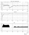
- the invention has been tested and simulated on a functional model realized in a SIMULINK environment. This has permitted the reproduction of the waveforms of the significant current and voltage signals and a comparison between the behaviors of the converter with and without the modulator of the invention.
- Fig. 6 depicts the waveforms of the current output by the error amplifier of the output voltage and of the current through the power switch at start-up, with an applied load of about 40W under the control of the primary loop, of the flyback switching converter of in Fig. 3, in which the energy transfer modulator block MODULATOR of the invention had been introduced.
- Fig. 7 shows the waveforms of the same signals without a modulator block of the invention.
- Figures 8 and 9 show the waveforms of the same signals for a converter with and without the modulator block, respectively, these waveforms highlight the transient that occurs at start-up with a 200W load, until about 20ms, and upon a stepwise is reduction of the load to about 4W.
Priority Applications (4)
| Application Number | Priority Date | Filing Date | Title |
|---|---|---|---|
| DE69810625T DE69810625T2 (de) | 1998-10-07 | 1998-10-07 | Leistungsübertragungssteueurung in Sperrwandler durch lastabhängige Austastmodulation |
| EP98830591A EP0993105B1 (de) | 1998-10-07 | 1998-10-07 | Leistungsübertragungssteueurung in Sperrwandler durch lastabhängige Austastmodulation |
| JP28636299A JP4400958B2 (ja) | 1998-10-07 | 1999-10-07 | 負荷の関数におけるオフフェーズを変調することによりフライバック変換器における電力伝達の制御 |
| US09/413,996 US6118675A (en) | 1998-10-07 | 1999-10-07 | Method and apparatus for controlling power transfer in a flyback converter by modulating the power switch off time during transient conditions |
Applications Claiming Priority (1)
| Application Number | Priority Date | Filing Date | Title |
|---|---|---|---|
| EP98830591A EP0993105B1 (de) | 1998-10-07 | 1998-10-07 | Leistungsübertragungssteueurung in Sperrwandler durch lastabhängige Austastmodulation |
Publications (2)
| Publication Number | Publication Date |
|---|---|
| EP0993105A1 true EP0993105A1 (de) | 2000-04-12 |
| EP0993105B1 EP0993105B1 (de) | 2003-01-08 |
Family
ID=8236821
Family Applications (1)
| Application Number | Title | Priority Date | Filing Date |
|---|---|---|---|
| EP98830591A Expired - Lifetime EP0993105B1 (de) | 1998-10-07 | 1998-10-07 | Leistungsübertragungssteueurung in Sperrwandler durch lastabhängige Austastmodulation |
Country Status (4)
| Country | Link |
|---|---|
| US (1) | US6118675A (de) |
| EP (1) | EP0993105B1 (de) |
| JP (1) | JP4400958B2 (de) |
| DE (1) | DE69810625T2 (de) |
Cited By (14)
| Publication number | Priority date | Publication date | Assignee | Title |
|---|---|---|---|---|
| GB2366098A (en) * | 1999-01-28 | 2002-02-27 | Power One Ag | DC-AC-DC converter |
| FR2836762A1 (fr) * | 2002-03-01 | 2003-09-05 | Koito Mfg Co Ltd | Circuit de conversion de tension continue pour lampe a decharge |
| WO2003061106A3 (en) * | 2002-01-11 | 2004-01-15 | Sanken Electric Co Ltd | Power source apparatus |
| KR100418902B1 (ko) * | 2001-09-06 | 2004-02-14 | 엘지전자 주식회사 | 전원제어장치 |
| WO2004062073A1 (en) * | 2002-12-31 | 2004-07-22 | Intel Corporation | Load-dependent variable frequency voltage regulator |
| WO2006067522A2 (en) | 2004-12-21 | 2006-06-29 | Cambridge Semiconductor Limited | Power supply control system |
| WO2008115231A1 (en) * | 2007-03-19 | 2008-09-25 | Semiconductor Components Industries, L.L.C. | Method of forming a power supply controller and structure therefor |
| US7504815B2 (en) | 2005-07-06 | 2009-03-17 | Cambridge Semiconductor Limited | Switch mode power supply control systems |
| US7710098B2 (en) | 2005-12-16 | 2010-05-04 | Cambridge Semiconductor Limited | Power supply driver circuit |
| US7733098B2 (en) | 2005-12-22 | 2010-06-08 | Cambridge Semiconductor Limited | Saturation detection circuits |
| EP2210884A2 (de) | 2005-03-28 | 2010-07-28 | Toyama Chemical Co., Ltd. | Prozess zur Herstellung von 1-(3-(2-(1-Benzothiophen-5-yl)-ethoxy)propionsäure und 1-(3-(2-(1-Benzothiophen-5-yl)-ethoxy)propyl)azetidin-3-ol sowie deren Salze |
| CN101867299A (zh) * | 2010-07-20 | 2010-10-20 | 周光友 | 一种用于开关电源反馈电压检测和采样保持的电路及方法 |
| CN103078503A (zh) * | 2011-09-29 | 2013-05-01 | 电力集成公司 | 接通时间采样防止 |
| CN109951064A (zh) * | 2017-12-21 | 2019-06-28 | 美格纳半导体有限公司 | 高电压启动电路及开关模式电源 |
Families Citing this family (38)
| Publication number | Priority date | Publication date | Assignee | Title |
|---|---|---|---|---|
| KR100379057B1 (ko) * | 1999-04-10 | 2003-04-08 | 페어차일드코리아반도체 주식회사 | 버스트 모드 스위칭 모드 파워 서플라이 |
| WO2000074221A1 (en) * | 1999-05-26 | 2000-12-07 | Koninklijke Philips Electronics N.V. | Converter for the conversion of an input voltage into an output voltage |
| US6462971B1 (en) * | 1999-09-24 | 2002-10-08 | Power Integrations, Inc. | Method and apparatus providing a multi-function terminal for a power supply controller |
| KR100342590B1 (ko) * | 1999-10-06 | 2002-07-04 | 김덕중 | 펄스폭 변조 신호 발생 장치 및 이를 이용한 스위칭 모드 파워 서플라이 |
| JP3369134B2 (ja) * | 1999-11-16 | 2003-01-20 | サンケン電気株式会社 | Dc−dcコンバータ |
| FR2815790B1 (fr) * | 2000-10-24 | 2003-02-07 | St Microelectronics Sa | Convertisseur de tension a circuit de commande autooscillant |
| US6385060B1 (en) * | 2000-12-21 | 2002-05-07 | Semiconductor Components Industries Llc | Switching power supply with reduced energy transfer during a fault condition |
| JP3412624B2 (ja) * | 2001-06-08 | 2003-06-03 | サンケン電気株式会社 | スイッチング電源装置 |
| US6721192B1 (en) * | 2003-03-24 | 2004-04-13 | System General Corp. | PWM controller regulating output voltage and output current in primary side |
| US6865093B2 (en) * | 2003-05-27 | 2005-03-08 | Power Integrations, Inc. | Electronic circuit control element with tap element |
| US6853563B1 (en) * | 2003-07-28 | 2005-02-08 | System General Corp. | Primary-side controlled flyback power converter |
| US6977824B1 (en) * | 2004-08-09 | 2005-12-20 | System General Corp. | Control circuit for controlling output current at the primary side of a power converter |
| US7016204B2 (en) * | 2004-08-12 | 2006-03-21 | System General Corp. | Close-loop PWM controller for primary-side controlled power converters |
| US7362593B2 (en) * | 2004-09-16 | 2008-04-22 | System General Corp. | Switching control circuit having off-time modulation to improve efficiency of primary-side controlled power supply |
| US7362592B2 (en) * | 2004-09-16 | 2008-04-22 | System General Corp. | Switching control circuit for primary-side controlled power converters |
| US7259972B2 (en) * | 2004-10-07 | 2007-08-21 | System General Corporation | Primary-side-control power converter having a switching controller using frequency hopping and voltage and current control loops |
| US20060133115A1 (en) * | 2004-12-22 | 2006-06-22 | Phadke Vijay G | Adaptive blanking of transformer primary-side feedback winding signals |
| CN100466440C (zh) * | 2005-01-25 | 2009-03-04 | 技领半导体(上海)有限公司 | 一种控制开关电源输出电流的方法及电路 |
| JP4617931B2 (ja) * | 2005-03-07 | 2011-01-26 | 富士電機システムズ株式会社 | スイッチング電源回路の制御方式 |
| US7564903B2 (en) * | 2005-10-07 | 2009-07-21 | System General Corp. | Method and apparatus for measuring reflected voltage of transformer |
| CN101127495B (zh) * | 2006-08-16 | 2010-04-21 | 昂宝电子(上海)有限公司 | 用于为开关式电源提供控制的系统和方法 |
| TW200915709A (en) * | 2007-09-17 | 2009-04-01 | Richtek Technology Corp | Apparatus and method for regulating constant output voltage and current in a voltage flyback converter |
| AT507324B1 (de) * | 2008-10-02 | 2012-05-15 | Siemens Ag | Schaltwandler und verfahren zum betreiben des schaltwandlers |
| DE102009030740A1 (de) * | 2009-06-26 | 2010-12-30 | Siemens Aktiengesellschaft | Kommutierungsverfahren einer Stromrichterphase mit rückwärts leitfähigen IGBTs |
| CN101924471B (zh) * | 2010-08-31 | 2013-05-01 | 深圳市明微电子股份有限公司 | 恒定输出电流的方法及装置 |
| TWI403058B (zh) | 2010-11-30 | 2013-07-21 | Inventec Corp | 直流電壓供應裝置 |
| CN102480225B (zh) * | 2010-11-30 | 2014-03-12 | 英业达股份有限公司 | 直流电压供应装置 |
| WO2012113396A2 (en) * | 2011-02-23 | 2012-08-30 | Vkr Holding A/S | A power supply comprising a stand by feature |
| CN102843050B (zh) * | 2012-07-12 | 2015-07-22 | 上海新进半导体制造有限公司 | 改善开关电源系统输出特性的方法和电路 |
| CN103347334A (zh) * | 2013-06-27 | 2013-10-09 | 浙江生辉照明有限公司 | 一种led照明装置的驱动电路及驱动方法 |
| TWI497889B (zh) * | 2013-07-23 | 2015-08-21 | Leadtrend Tech Corp | 用以降低電源轉換器的觸碰電流的控制電路及其操作方法 |
| TWI533579B (zh) * | 2014-10-01 | 2016-05-11 | 財團法人工業技術研究院 | 換流器輸出功率調節方法 |
| KR101755122B1 (ko) * | 2015-11-02 | 2017-07-06 | 현대자동차주식회사 | Dc-ac 컨버터 제어 방법과 이를 사용하는 그라운드 어셈블리 및 무선 전력 전송 방법 |
| US10199918B2 (en) | 2017-07-10 | 2019-02-05 | Semiconductor Components Industries, Llc | Method of forming a semiconductor device |
| CN109995254B (zh) * | 2017-12-29 | 2020-12-29 | 东南大学 | 一种提高同步整流原边反馈反激式电源动态性能的方法 |
| CN112630821B (zh) * | 2020-12-30 | 2024-01-12 | 核工业北京地质研究院 | 一种应用于地震数据采集的变频控制装置及其控制方法 |
| CN112838772B (zh) * | 2021-01-18 | 2022-05-13 | 昂宝电子(上海)有限公司 | 反激式开关电源及其控制方法 |
| CN113258784B (zh) * | 2021-06-08 | 2022-12-16 | 成都芯源系统有限公司 | 一种开关电源的供电电源电路及其控制方法 |
Citations (3)
| Publication number | Priority date | Publication date | Assignee | Title |
|---|---|---|---|---|
| US4984145A (en) * | 1989-01-25 | 1991-01-08 | Siemens Aktiengesellschaft | Circuit arrangement for free-running blocking-oscillator type switched power pack |
| US5657215A (en) * | 1995-08-29 | 1997-08-12 | Compaq Computer Corporation | Controlling switch-Mode power conversion |
| US5748461A (en) * | 1994-10-19 | 1998-05-05 | Siemens Aktiengesellschaft | SMPS with low load switching frequency stabilization |
-
1998
- 1998-10-07 DE DE69810625T patent/DE69810625T2/de not_active Expired - Fee Related
- 1998-10-07 EP EP98830591A patent/EP0993105B1/de not_active Expired - Lifetime
-
1999
- 1999-10-07 US US09/413,996 patent/US6118675A/en not_active Expired - Lifetime
- 1999-10-07 JP JP28636299A patent/JP4400958B2/ja not_active Expired - Fee Related
Patent Citations (3)
| Publication number | Priority date | Publication date | Assignee | Title |
|---|---|---|---|---|
| US4984145A (en) * | 1989-01-25 | 1991-01-08 | Siemens Aktiengesellschaft | Circuit arrangement for free-running blocking-oscillator type switched power pack |
| US5748461A (en) * | 1994-10-19 | 1998-05-05 | Siemens Aktiengesellschaft | SMPS with low load switching frequency stabilization |
| US5657215A (en) * | 1995-08-29 | 1997-08-12 | Compaq Computer Corporation | Controlling switch-Mode power conversion |
Cited By (22)
| Publication number | Priority date | Publication date | Assignee | Title |
|---|---|---|---|---|
| GB2366098B (en) * | 1999-01-28 | 2002-07-31 | Power One Ag | Voltage converter |
| GB2366098A (en) * | 1999-01-28 | 2002-02-27 | Power One Ag | DC-AC-DC converter |
| KR100418902B1 (ko) * | 2001-09-06 | 2004-02-14 | 엘지전자 주식회사 | 전원제어장치 |
| US7154762B2 (en) | 2002-01-11 | 2006-12-26 | Sanken Electric Co., Ltd. | Power source apparatus |
| WO2003061106A3 (en) * | 2002-01-11 | 2004-01-15 | Sanken Electric Co Ltd | Power source apparatus |
| FR2836762A1 (fr) * | 2002-03-01 | 2003-09-05 | Koito Mfg Co Ltd | Circuit de conversion de tension continue pour lampe a decharge |
| US7046528B2 (en) | 2002-12-31 | 2006-05-16 | Intel Corporation | Load-dependent variable frequency voltage regulator |
| WO2004062073A1 (en) * | 2002-12-31 | 2004-07-22 | Intel Corporation | Load-dependent variable frequency voltage regulator |
| WO2006067522A2 (en) | 2004-12-21 | 2006-06-29 | Cambridge Semiconductor Limited | Power supply control system |
| WO2006067522A3 (en) * | 2004-12-21 | 2007-03-29 | Cambridge Semiconductor Ltd | Power supply control system |
| EP2210884A2 (de) | 2005-03-28 | 2010-07-28 | Toyama Chemical Co., Ltd. | Prozess zur Herstellung von 1-(3-(2-(1-Benzothiophen-5-yl)-ethoxy)propionsäure und 1-(3-(2-(1-Benzothiophen-5-yl)-ethoxy)propyl)azetidin-3-ol sowie deren Salze |
| US7504815B2 (en) | 2005-07-06 | 2009-03-17 | Cambridge Semiconductor Limited | Switch mode power supply control systems |
| US7710098B2 (en) | 2005-12-16 | 2010-05-04 | Cambridge Semiconductor Limited | Power supply driver circuit |
| US7733098B2 (en) | 2005-12-22 | 2010-06-08 | Cambridge Semiconductor Limited | Saturation detection circuits |
| WO2008115231A1 (en) * | 2007-03-19 | 2008-09-25 | Semiconductor Components Industries, L.L.C. | Method of forming a power supply controller and structure therefor |
| CN101867299A (zh) * | 2010-07-20 | 2010-10-20 | 周光友 | 一种用于开关电源反馈电压检测和采样保持的电路及方法 |
| CN101867299B (zh) * | 2010-07-20 | 2012-03-21 | 周光友 | 一种用于开关电源反馈电压检测和采样保持的电路及方法 |
| CN103078503A (zh) * | 2011-09-29 | 2013-05-01 | 电力集成公司 | 接通时间采样防止 |
| CN103078503B (zh) * | 2011-09-29 | 2015-08-26 | 电力集成公司 | 接通时间采样防止 |
| US9287787B2 (en) | 2011-09-29 | 2016-03-15 | Power Integrations, Inc. | On time sampling prevention |
| CN109951064A (zh) * | 2017-12-21 | 2019-06-28 | 美格纳半导体有限公司 | 高电压启动电路及开关模式电源 |
| CN109951064B (zh) * | 2017-12-21 | 2021-01-05 | 美格纳半导体有限公司 | 高电压启动电路及开关模式电源 |
Also Published As
| Publication number | Publication date |
|---|---|
| JP2000125561A (ja) | 2000-04-28 |
| EP0993105B1 (de) | 2003-01-08 |
| DE69810625T2 (de) | 2003-11-27 |
| JP4400958B2 (ja) | 2010-01-20 |
| US6118675A (en) | 2000-09-12 |
| DE69810625D1 (de) | 2003-02-13 |
Similar Documents
| Publication | Publication Date | Title |
|---|---|---|
| EP0993105B1 (de) | Leistungsübertragungssteueurung in Sperrwandler durch lastabhängige Austastmodulation | |
| US8994351B2 (en) | Smooth mode transition plateau for a power supply controller | |
| US7826237B2 (en) | Method and system for efficient power control with multiple modes | |
| US6545882B2 (en) | PWM controller having off-time modulation for power converter | |
| US8270184B2 (en) | Isolated voltage converter with feedback on the primary winding and passive snubber network, and corresponding control method | |
| US8970198B2 (en) | Switch-mode power supply having reduced audible noise | |
| US6208538B1 (en) | PWM control apparatus | |
| US9048742B2 (en) | Systems and methods for adjusting current consumption of control chips to reduce standby power consumption of power converters | |
| US7286376B2 (en) | Soft-switching power converter having power saving circuit for light load operations | |
| US6069804A (en) | Bi-directional dc-to-dc power converter | |
| US5677619A (en) | Method and apparatus for multiple output regulation in a step-down switching regulator | |
| US9531279B2 (en) | Power supply controller with minimum-sum multi-cycle modulation | |
| US5734564A (en) | High-efficiency switching power converter | |
| KR100398565B1 (ko) | 플라이백변환기 | |
| TWI672896B (zh) | 主動鉗位反馳式電源轉換器與相關之控制方法 | |
| KR100411327B1 (ko) | 다중 전압 출력을 갖는 전원 장치를 구비하는 다중 모드모니터 | |
| US6084784A (en) | Switched mode power supply with reduced reflected power | |
| EP2299579B1 (de) | Erweiterung des erzielbaren Arbeitszyklusbereichs in einem Gleichstrom-Durchflusswandler mit Active Clamp/Reset | |
| JP2769451B2 (ja) | 量子化電力変換装置 | |
| Levin | A new secondary side post regulator (SSPR) PWM controller for multiple output power supplies | |
| CN1938924B (zh) | 具有用于节省功率和减少噪声的调制器的pwm控制器 | |
| US6072702A (en) | Ringing choke converter | |
| CN111030479B (zh) | 有源钳位反激式电源转换器与相关的控制方法 | |
| CN113632354A (zh) | 谐振转换器的软启动 | |
| US6208089B1 (en) | Discharge-lamp lighting circuit |
Legal Events
| Date | Code | Title | Description |
|---|---|---|---|
| PUAI | Public reference made under article 153(3) epc to a published international application that has entered the european phase |
Free format text: ORIGINAL CODE: 0009012 |
|
| AK | Designated contracting states |
Kind code of ref document: A1 Designated state(s): DE FR GB IT |
|
| AX | Request for extension of the european patent |
Free format text: AL;LT;LV;MK;RO;SI |
|
| 17P | Request for examination filed |
Effective date: 20000427 |
|
| AKX | Designation fees paid |
Free format text: DE FR GB IT |
|
| GRAG | Despatch of communication of intention to grant |
Free format text: ORIGINAL CODE: EPIDOS AGRA |
|
| 17Q | First examination report despatched |
Effective date: 20020314 |
|
| GRAG | Despatch of communication of intention to grant |
Free format text: ORIGINAL CODE: EPIDOS AGRA |
|
| GRAH | Despatch of communication of intention to grant a patent |
Free format text: ORIGINAL CODE: EPIDOS IGRA |
|
| GRAH | Despatch of communication of intention to grant a patent |
Free format text: ORIGINAL CODE: EPIDOS IGRA |
|
| GRAA | (expected) grant |
Free format text: ORIGINAL CODE: 0009210 |
|
| AK | Designated contracting states |
Kind code of ref document: B1 Designated state(s): DE FR GB IT |
|
| REG | Reference to a national code |
Ref country code: GB Ref legal event code: FG4D |
|
| REF | Corresponds to: |
Ref document number: 69810625 Country of ref document: DE Date of ref document: 20030213 Kind code of ref document: P |
|
| ET | Fr: translation filed | ||
| PLBE | No opposition filed within time limit |
Free format text: ORIGINAL CODE: 0009261 |
|
| STAA | Information on the status of an ep patent application or granted ep patent |
Free format text: STATUS: NO OPPOSITION FILED WITHIN TIME LIMIT |
|
| 26N | No opposition filed |
Effective date: 20031009 |
|
| PGFP | Annual fee paid to national office [announced via postgrant information from national office to epo] |
Ref country code: DE Payment date: 20060928 Year of fee payment: 9 |
|
| PGFP | Annual fee paid to national office [announced via postgrant information from national office to epo] |
Ref country code: IT Payment date: 20061031 Year of fee payment: 9 |
|
| PGFP | Annual fee paid to national office [announced via postgrant information from national office to epo] |
Ref country code: FR Payment date: 20071030 Year of fee payment: 10 |
|
| PG25 | Lapsed in a contracting state [announced via postgrant information from national office to epo] |
Ref country code: DE Free format text: LAPSE BECAUSE OF NON-PAYMENT OF DUE FEES Effective date: 20080501 |
|
| REG | Reference to a national code |
Ref country code: FR Ref legal event code: ST Effective date: 20090630 |
|
| PG25 | Lapsed in a contracting state [announced via postgrant information from national office to epo] |
Ref country code: IT Free format text: LAPSE BECAUSE OF NON-PAYMENT OF DUE FEES Effective date: 20071007 |
|
| PG25 | Lapsed in a contracting state [announced via postgrant information from national office to epo] |
Ref country code: FR Free format text: LAPSE BECAUSE OF NON-PAYMENT OF DUE FEES Effective date: 20081031 |
|
| PGFP | Annual fee paid to national office [announced via postgrant information from national office to epo] |
Ref country code: GB Payment date: 20120924 Year of fee payment: 15 |
|
| GBPC | Gb: european patent ceased through non-payment of renewal fee |
Effective date: 20131007 |
|
| PG25 | Lapsed in a contracting state [announced via postgrant information from national office to epo] |
Ref country code: GB Free format text: LAPSE BECAUSE OF NON-PAYMENT OF DUE FEES Effective date: 20131007 |