EP0985159B1 - Integrierte optische schaltung - Google Patents
Integrierte optische schaltung Download PDFInfo
- Publication number
- EP0985159B1 EP0985159B1 EP98922783A EP98922783A EP0985159B1 EP 0985159 B1 EP0985159 B1 EP 0985159B1 EP 98922783 A EP98922783 A EP 98922783A EP 98922783 A EP98922783 A EP 98922783A EP 0985159 B1 EP0985159 B1 EP 0985159B1
- Authority
- EP
- European Patent Office
- Prior art keywords
- photonic crystal
- integrated optical
- optical circuit
- waveguides
- circuit according
- Prior art date
- Legal status (The legal status is an assumption and is not a legal conclusion. Google has not performed a legal analysis and makes no representation as to the accuracy of the status listed.)
- Expired - Lifetime
Links
- 230000003287 optical effect Effects 0.000 title claims abstract description 32
- 239000004038 photonic crystal Substances 0.000 claims abstract description 38
- XUIMIQQOPSSXEZ-UHFFFAOYSA-N Silicon Chemical compound [Si] XUIMIQQOPSSXEZ-UHFFFAOYSA-N 0.000 claims abstract description 11
- 229910052710 silicon Inorganic materials 0.000 claims abstract description 11
- 239000010703 silicon Substances 0.000 claims abstract description 11
- 239000000758 substrate Substances 0.000 claims abstract description 9
- 239000000463 material Substances 0.000 claims description 10
- 230000000737 periodic effect Effects 0.000 claims description 4
- 238000005259 measurement Methods 0.000 description 4
- 238000000034 method Methods 0.000 description 3
- 238000011161 development Methods 0.000 description 2
- 230000000694 effects Effects 0.000 description 2
- 238000005516 engineering process Methods 0.000 description 2
- 230000004907 flux Effects 0.000 description 2
- 239000012535 impurity Substances 0.000 description 2
- 229920000642 polymer Polymers 0.000 description 2
- 239000004065 semiconductor Substances 0.000 description 2
- VYPSYNLAJGMNEJ-UHFFFAOYSA-N Silicium dioxide Chemical compound O=[Si]=O VYPSYNLAJGMNEJ-UHFFFAOYSA-N 0.000 description 1
- 239000000654 additive Substances 0.000 description 1
- 238000004891 communication Methods 0.000 description 1
- 230000000295 complement effect Effects 0.000 description 1
- 150000001875 compounds Chemical class 0.000 description 1
- 239000013078 crystal Substances 0.000 description 1
- 238000013016 damping Methods 0.000 description 1
- 230000007547 defect Effects 0.000 description 1
- 230000001419 dependent effect Effects 0.000 description 1
- 230000008021 deposition Effects 0.000 description 1
- 238000009826 distribution Methods 0.000 description 1
- 238000000609 electron-beam lithography Methods 0.000 description 1
- 238000002474 experimental method Methods 0.000 description 1
- 238000003780 insertion Methods 0.000 description 1
- 230000037431 insertion Effects 0.000 description 1
- 238000001459 lithography Methods 0.000 description 1
- 238000004519 manufacturing process Methods 0.000 description 1
- 230000002093 peripheral effect Effects 0.000 description 1
- 230000010363 phase shift Effects 0.000 description 1
- 238000012552 review Methods 0.000 description 1
- 229910052814 silicon oxide Inorganic materials 0.000 description 1
- 230000003595 spectral effect Effects 0.000 description 1
- 238000012360 testing method Methods 0.000 description 1
Images

Classifications
-
- G—PHYSICS
- G02—OPTICS
- G02F—OPTICAL DEVICES OR ARRANGEMENTS FOR THE CONTROL OF LIGHT BY MODIFICATION OF THE OPTICAL PROPERTIES OF THE MEDIA OF THE ELEMENTS INVOLVED THEREIN; NON-LINEAR OPTICS; FREQUENCY-CHANGING OF LIGHT; OPTICAL LOGIC ELEMENTS; OPTICAL ANALOGUE/DIGITAL CONVERTERS
- G02F1/00—Devices or arrangements for the control of the intensity, colour, phase, polarisation or direction of light arriving from an independent light source, e.g. switching, gating or modulating; Non-linear optics
- G02F1/01—Devices or arrangements for the control of the intensity, colour, phase, polarisation or direction of light arriving from an independent light source, e.g. switching, gating or modulating; Non-linear optics for the control of the intensity, phase, polarisation or colour
- G02F1/21—Devices or arrangements for the control of the intensity, colour, phase, polarisation or direction of light arriving from an independent light source, e.g. switching, gating or modulating; Non-linear optics for the control of the intensity, phase, polarisation or colour by interference
- G02F1/225—Devices or arrangements for the control of the intensity, colour, phase, polarisation or direction of light arriving from an independent light source, e.g. switching, gating or modulating; Non-linear optics for the control of the intensity, phase, polarisation or colour by interference in an optical waveguide structure
-
- B—PERFORMING OPERATIONS; TRANSPORTING
- B82—NANOTECHNOLOGY
- B82Y—SPECIFIC USES OR APPLICATIONS OF NANOSTRUCTURES; MEASUREMENT OR ANALYSIS OF NANOSTRUCTURES; MANUFACTURE OR TREATMENT OF NANOSTRUCTURES
- B82Y20/00—Nanooptics, e.g. quantum optics or photonic crystals
-
- G—PHYSICS
- G02—OPTICS
- G02B—OPTICAL ELEMENTS, SYSTEMS OR APPARATUS
- G02B6/00—Light guides; Structural details of arrangements comprising light guides and other optical elements, e.g. couplings
- G02B6/10—Light guides; Structural details of arrangements comprising light guides and other optical elements, e.g. couplings of the optical waveguide type
- G02B6/12—Light guides; Structural details of arrangements comprising light guides and other optical elements, e.g. couplings of the optical waveguide type of the integrated circuit kind
- G02B6/122—Basic optical elements, e.g. light-guiding paths
- G02B6/1225—Basic optical elements, e.g. light-guiding paths comprising photonic band-gap structures or photonic lattices
-
- G—PHYSICS
- G02—OPTICS
- G02F—OPTICAL DEVICES OR ARRANGEMENTS FOR THE CONTROL OF LIGHT BY MODIFICATION OF THE OPTICAL PROPERTIES OF THE MEDIA OF THE ELEMENTS INVOLVED THEREIN; NON-LINEAR OPTICS; FREQUENCY-CHANGING OF LIGHT; OPTICAL LOGIC ELEMENTS; OPTICAL ANALOGUE/DIGITAL CONVERTERS
- G02F1/00—Devices or arrangements for the control of the intensity, colour, phase, polarisation or direction of light arriving from an independent light source, e.g. switching, gating or modulating; Non-linear optics
- G02F1/01—Devices or arrangements for the control of the intensity, colour, phase, polarisation or direction of light arriving from an independent light source, e.g. switching, gating or modulating; Non-linear optics for the control of the intensity, phase, polarisation or colour
- G02F1/011—Devices or arrangements for the control of the intensity, colour, phase, polarisation or direction of light arriving from an independent light source, e.g. switching, gating or modulating; Non-linear optics for the control of the intensity, phase, polarisation or colour in optical waveguides, not otherwise provided for in this subclass
-
- G—PHYSICS
- G02—OPTICS
- G02F—OPTICAL DEVICES OR ARRANGEMENTS FOR THE CONTROL OF LIGHT BY MODIFICATION OF THE OPTICAL PROPERTIES OF THE MEDIA OF THE ELEMENTS INVOLVED THEREIN; NON-LINEAR OPTICS; FREQUENCY-CHANGING OF LIGHT; OPTICAL LOGIC ELEMENTS; OPTICAL ANALOGUE/DIGITAL CONVERTERS
- G02F1/00—Devices or arrangements for the control of the intensity, colour, phase, polarisation or direction of light arriving from an independent light source, e.g. switching, gating or modulating; Non-linear optics
- G02F1/01—Devices or arrangements for the control of the intensity, colour, phase, polarisation or direction of light arriving from an independent light source, e.g. switching, gating or modulating; Non-linear optics for the control of the intensity, phase, polarisation or colour
- G02F1/21—Devices or arrangements for the control of the intensity, colour, phase, polarisation or direction of light arriving from an independent light source, e.g. switching, gating or modulating; Non-linear optics for the control of the intensity, phase, polarisation or colour by interference
- G02F1/212—Mach-Zehnder type
-
- G—PHYSICS
- G02—OPTICS
- G02F—OPTICAL DEVICES OR ARRANGEMENTS FOR THE CONTROL OF LIGHT BY MODIFICATION OF THE OPTICAL PROPERTIES OF THE MEDIA OF THE ELEMENTS INVOLVED THEREIN; NON-LINEAR OPTICS; FREQUENCY-CHANGING OF LIGHT; OPTICAL LOGIC ELEMENTS; OPTICAL ANALOGUE/DIGITAL CONVERTERS
- G02F2202/00—Materials and properties
- G02F2202/32—Photonic crystals
Definitions
- the invention relates to an integrated optical circuit with a silicon substrate and arranged thereon Waveguides with at least one photonic crystal.
- Integrated optical circuits are used in the Communication technology needed for different purposes for example for distribution, summary, spectral Splitting or switching with information modulated luminous flux.
- others can Circuits implemented using optical structures are, for example computer circuits.
- Integrated optical circuits are currently being used Polymer waveguides or III-V compound semiconductors built by lithographic processes are structured.
- Such waveguide patterns are usually polymer or striped waveguides Semiconductor material.
- These waveguide patterns can be complementary Structure are generated that spread the Photon pulses in matter by their embodiment prevent and spread by targeted built-in Defects in otherwise completely reflective matter.
- a jump in the refractive index is not the same as with leadership of waves in optical waveguides by doping or are designed as strip waveguides, but here - theoretically given - forbidden bands limit the State solution of the desired for certain wavelengths In-house solutions for the propagation of these waves.
- the Description of this waveguide is for example from Mekis A. et al in Physical Review Letters, Volume 77, No. 18, p. 3787.
- Such two-dimensional photonic crystals can be used as Filters are used, for example in Koops, Hans W.P .: "Photonic Crystals Built by Three-dimensional Additives Lithography Enable Integrated Optics of High Density ", Proceedings of the SPIE, volume 2849, August 5, 1996, pages 248 to 256. Individuals become spatial distributed elements (wires) of the photonic crystals different material. Furthermore are three-dimensional photonic crystals by Cheng C C et al .: Fabrication PF Photonic Band-Gap Crystals' Journal of Vacuum Science and Technology: Part B, Volume 13, No. 6, 01. November 1995, pages 2696 to 2700.
- the object of the present invention is an integrated specify optical circuit when using photonic Crystals formed waveguides for wavelength dependent Reflections from the substrate level are applied and that can be manufactured with the required precision.
- silicon Isolator is well transmissive for wavelengths of 1.55 ⁇ m.
- silicon has a very high one with these waveguides Dielectric constant of 12, which is also the case with the photonic crystals can be used.
- special photonic crystals ensure the function of the circuit, for example as Arithmetic circuit, the entire circuit being very small can be executed. For example, there are 6 periods of the lattice of photonic crystals with a Grid spacing of 1/3 of the wavelength is sufficient to achieve a To achieve attenuation of 35 dB.
- An advantageous embodiment of the invention Circuit is that the elements of at least a photonic crystal with a high needles Dielectric constants are in the form of a two-dimensional periodic grating are arranged. It is also quite possible that the elements of the at least one photonic crystal holes lower Dielectric constant in a body with a high Dielectric constants are in the form of a two-dimensional periodic grating are arranged.
- the needles are on the insulating layer that in the area of the photonic crystal is less strong than below the waveguides, or that the needles on the Silicon substrate stand.
- An advantageous development of the invention Circuit is that the gaps between the Needles are filled with non-linear optical material and that with the help of one applied to field electrodes Voltage the refractive index of the non-linear optical Material is adjustable. This is a control For example, the behavior of filters that can be viewed as Integrated optical circuits are implemented, see also DE 196 34 893 A1.
- the at least one photonic crystal by the arrangement the impurities represent a branch filter in which branched light of a selected wavelength range emerges laterally and the rest of the light in the photonic Crystal is forwarded.
- the side exiting Light can be transmitted in a variety of ways.
- Fig. 1 is on an insulating layer 2 from a silicon substrate 1 Silicon oxide, on which optical strip waveguide 3, 4 are applied from silicon. Between the waveguides 3, 4 there is a photonic crystal 5, which of a grid of needles 6 is formed.
- the needles 6 are in the embodiment on the Insulating layer 2 in the area of the photonic crystal 5 has a cavity. Because of this and that the needles over the protrude the upper boundary plane of the waveguides 3, 4, the photonic crystal also does that in peripheral areas field guided outside the waveguide is detected.
- the needles 6 can pass through in a manner known per se Corpuscular beam deposition can be made. On The method for this is described, for example, in DE 195 33 148 A1.
- Fig. 4 shows an embodiment in which the photonic crystal forming needles 14 are inclined.
- a cover layer 15 is placed on selected areas, so that light exits there and 16 through attached lenses preferably polymeric material in not shown Entry window focused on a level above becomes.
- the lenses can in a known manner with electron beam lithography or be generated with optical methods.
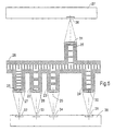
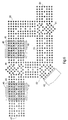
- Fig. 5 shows a section of an inventive Circuit in which a plurality of branches 21 to 25 of a photonic crystal 26, one being Lens 27 to 31 on the light emerging from the branch Entry areas 32 to 36 focused on next to the photonic crystal 26 extending further optical Elements 37, 38 are arranged.
- FIG. 6 shows a Mach-Zehnder interferometer trained embodiment. All elements are especially waveguides, filters, mirrors and Beam splitter formed by photonic crystals. With the Interferometer is said to reflect the transit time in a Fig. 6 only indicated measurement object 41 can be measured.
- the light supplied at 42 is first of all adjustable filter 43 passed, with the help of Measurement to be used is selected.
- the end the filter 43 emerging light is by means of a Beam splitter 44 in equal parts straight to one adjustable phase shifter 45 and reflected to Object 41 passed.
- the adjustable filter 43 and the adjustable one Phase shifters 45 each consist of a photonic Crystal, the spaces with non-linear optical Material are filled, its dielectric constant and thus the optically effective distances between the needles With the help of electrodes 46, 47 and 48, 49, respectively Voltages are controllable.
- the phase shifter 45 is completely closed reflective mirror 50, which from the Phase shifter 45 emerging light another Beam splitter 51 supplies.
- a direction switch 42 trained photonic crystal arranged with the Effect that the light arriving from the beam splitter 44 in the object 41 is guided and that in the measurement object reflected light via a waveguide 43 for further Beam splitter 51 arrives.
- exit 54 overlap both luminous fluxes.
- a suitable transducer can measure the intensity emerging from the output 54 and by setting the phase at 45 to a minimum of Intensity at output 54 is the phase shift in the test object 41 can be determined.
- the circuit shown in FIG. 6 can also be extremely small be interpreted, for example with an entire length of about 20 ⁇ m.
Landscapes
- Physics & Mathematics (AREA)
- Optics & Photonics (AREA)
- Engineering & Computer Science (AREA)
- Chemical & Material Sciences (AREA)
- General Physics & Mathematics (AREA)
- Nonlinear Science (AREA)
- Nanotechnology (AREA)
- Life Sciences & Earth Sciences (AREA)
- Biophysics (AREA)
- Crystallography & Structural Chemistry (AREA)
- Microelectronics & Electronic Packaging (AREA)
- Optical Integrated Circuits (AREA)
- Optical Couplings Of Light Guides (AREA)
Applications Claiming Priority (3)
| Application Number | Priority Date | Filing Date | Title |
|---|---|---|---|
| DE19720784A DE19720784A1 (de) | 1997-05-17 | 1997-05-17 | Integrierte optische Schaltung |
| DE19720784 | 1997-05-17 | ||
| PCT/EP1998/002532 WO1998053350A1 (de) | 1997-05-17 | 1998-04-29 | Integrierte optische schaltung |
Publications (2)
| Publication Number | Publication Date |
|---|---|
| EP0985159A1 EP0985159A1 (de) | 2000-03-15 |
| EP0985159B1 true EP0985159B1 (de) | 2001-10-24 |
Family
ID=7829800
Family Applications (1)
| Application Number | Title | Priority Date | Filing Date |
|---|---|---|---|
| EP98922783A Expired - Lifetime EP0985159B1 (de) | 1997-05-17 | 1998-04-29 | Integrierte optische schaltung |
Country Status (9)
| Country | Link |
|---|---|
| US (1) | US6310991B1 (enExample) |
| EP (1) | EP0985159B1 (enExample) |
| JP (1) | JP4146520B2 (enExample) |
| AT (1) | ATE207622T1 (enExample) |
| AU (1) | AU740986B2 (enExample) |
| CA (1) | CA2289201C (enExample) |
| DE (2) | DE19720784A1 (enExample) |
| NZ (1) | NZ337209A (enExample) |
| WO (1) | WO1998053350A1 (enExample) |
Families Citing this family (45)
| Publication number | Priority date | Publication date | Assignee | Title |
|---|---|---|---|---|
| US6735368B2 (en) * | 1997-05-16 | 2004-05-11 | Mesophotonics Limited | Optical delay device |
| US6788863B2 (en) | 1997-05-16 | 2004-09-07 | Mesophotonics Limited | Optical delay device |
| GB9710062D0 (en) * | 1997-05-16 | 1997-07-09 | British Tech Group | Optical devices and methods of fabrication thereof |
| JP3200629B2 (ja) | 1999-08-11 | 2001-08-20 | 独立行政法人通信総合研究所 | フォトニックバンドギャップ構造を用いた光変調器及び光変調方法 |
| JP2001141946A (ja) * | 1999-11-16 | 2001-05-25 | Oki Electric Ind Co Ltd | 合分波素子 |
| JP2001281714A (ja) * | 2000-01-24 | 2001-10-10 | Minolta Co Ltd | 光機能素子及び光集積化素子 |
| CA2417747C (en) * | 2000-07-31 | 2009-11-24 | Naomi Matsuura | Configurable photonic device |
| US6674949B2 (en) * | 2000-08-15 | 2004-01-06 | Corning Incorporated | Active photonic crystal waveguide device and method |
| US6684008B2 (en) | 2000-09-01 | 2004-01-27 | The University Of British Columbia | Planar photonic bandgap structures for controlling radiation loss |
| JP2004510184A (ja) * | 2000-09-25 | 2004-04-02 | ブッカム テクノロジー パブリック リミテッド カンパニー | 人工的に構造化された誘電体材料 |
| JP3586635B2 (ja) * | 2000-10-19 | 2004-11-10 | 株式会社日立製作所 | 光デバイスおよび基板 |
| DE60127729T2 (de) * | 2000-12-27 | 2007-12-27 | Nippon Telegraph And Telephone Corp. | Photonenkristall-Wellenleiter |
| US6778722B1 (en) * | 2001-04-25 | 2004-08-17 | Raytheon Company | Method and apparatus for switching optical signals with a photon band gap device |
| US6936854B2 (en) | 2001-05-10 | 2005-08-30 | Canon Kabushiki Kaisha | Optoelectronic substrate |
| WO2002093248A1 (en) * | 2001-05-15 | 2002-11-21 | Massachussets Institute Of Technology | Mach-zehnder interferometer using photonic band gap crystals |
| EP1402564B1 (en) * | 2001-05-17 | 2017-07-12 | Cisco Technology, Inc. | Integrated optical/electronic circuits and associated methods of simultaneous generation thereof |
| US6775430B2 (en) | 2001-09-04 | 2004-08-10 | Agilent Technologies, Inc. | Photonic crystal interferometric switch |
| US6782169B2 (en) | 2001-09-05 | 2004-08-24 | University Of Delaware | System for efficient coupling to photonic crystal waveguides |
| US7194174B2 (en) * | 2001-10-19 | 2007-03-20 | Ignis Technologies As | Integrated photonic crystal structure and method of producing same |
| FR2832224B1 (fr) * | 2001-11-15 | 2004-01-16 | Commissariat Energie Atomique | Dispositif electronique monolithique multicouches et procede de realisation d'un tel dispositif |
| US6760514B2 (en) * | 2002-02-27 | 2004-07-06 | Agilent Technologies, Inc. | Continuously tunable photonic crystal drop filter |
| EP1341032A1 (de) * | 2002-02-28 | 2003-09-03 | Alcatel | Optischer Modulator aus photonischen Kristallen |
| GB0208255D0 (en) * | 2002-04-10 | 2002-05-22 | Imec Inter Uni Micro Electr | Photonic crystal based fiber-to-waveguide coupler for polarisation independent photonic integrated circuits |
| US6947649B2 (en) * | 2002-05-31 | 2005-09-20 | Matsushita Electric Industrial Co., Ltd. | Method of adjusting the index of refraction of photonic crystals with laser micromachining to tune transmissions within the bandgap and structure |
| US6940637B2 (en) | 2002-09-09 | 2005-09-06 | Battelle Memorial Institute | Multi-barrier photonic heterostructures |
| US6934441B2 (en) | 2003-09-09 | 2005-08-23 | Battelle Memorial Institute | Wavelength separation devices incorporating multi-barrier photonic heterostructures |
| AU2003270490A1 (en) * | 2002-09-09 | 2004-03-29 | Battelle Memorial Institute | Wavelength separation devices incorporating multi-barrier photonic heterostructures |
| GB2393264A (en) * | 2002-09-19 | 2004-03-24 | Univ Bristol | Optical photonic crystal waveguide filter |
| US6873777B2 (en) * | 2003-03-10 | 2005-03-29 | Japan Aviation Electronics Industry Limited | Two-dimensional photonic crystal device |
| US6990280B2 (en) | 2003-08-23 | 2006-01-24 | Hewlett-Packard Development Company, L.P. | Optical path with electrically conductive cladding |
| US7356215B2 (en) * | 2003-08-23 | 2008-04-08 | Hewlett-Packard Development Company, L.P. | Methods and apparatus for selectively coupling optical paths |
| US20050041946A1 (en) * | 2003-08-23 | 2005-02-24 | Deblanc James J. | Planar layer with optical path |
| DE10341030A1 (de) * | 2003-09-03 | 2005-04-07 | Christian-Albrechts-Universität Zu Kiel | Verfahren zur Herstellung von integrierten Wellenleitern |
| US7343059B2 (en) * | 2003-10-11 | 2008-03-11 | Hewlett-Packard Development Company, L.P. | Photonic interconnect system |
| FR2861854B1 (fr) * | 2003-10-30 | 2006-01-13 | Centre Nat Rech Scient | Dispositif de couplage-decouplage de lumiere selectif en frequence |
| JP3881666B2 (ja) * | 2004-03-25 | 2007-02-14 | 国立大学法人京都大学 | ヘテロ構造を有するフォトニック結晶及びそれを用いた光デバイス |
| JP4909528B2 (ja) * | 2005-04-18 | 2012-04-04 | 株式会社リコー | 光制御素子 |
| US7545999B2 (en) * | 2005-11-01 | 2009-06-09 | Hewlett-Packard Development Company, L.P. | Photonic configuration |
| WO2010073708A1 (ja) * | 2008-12-26 | 2010-07-01 | 日本電気株式会社 | 波長フィルタ |
| US9874688B2 (en) | 2012-04-26 | 2018-01-23 | Acacia Communications, Inc. | Co-packaging photonic integrated circuits and application specific integrated circuits |
| US9435959B2 (en) | 2012-04-26 | 2016-09-06 | Acacia Communications, Inc. | Coupling of fiber optics to planar grating couplers |
| USD758372S1 (en) | 2013-03-13 | 2016-06-07 | Nagrastar Llc | Smart card interface |
| US9888283B2 (en) | 2013-03-13 | 2018-02-06 | Nagrastar Llc | Systems and methods for performing transport I/O |
| SG11201703131WA (en) | 2014-10-29 | 2017-05-30 | Acacia Communications Inc | Optoelectronic ball grid array package with fiber |
| USD864968S1 (en) | 2015-04-30 | 2019-10-29 | Echostar Technologies L.L.C. | Smart card interface |
Family Cites Families (10)
| Publication number | Priority date | Publication date | Assignee | Title |
|---|---|---|---|---|
| DE3642897A1 (de) * | 1986-12-16 | 1988-06-30 | K O Prof Dr Thielheim | Doppelbrechendes optisches material und verfahren zu seiner herstellung |
| US5406573A (en) * | 1992-12-22 | 1995-04-11 | Iowa State University Research Foundation | Periodic dielectric structure for production of photonic band gap and method for fabricating the same |
| US5600483A (en) * | 1994-05-10 | 1997-02-04 | Massachusetts Institute Of Technology | Three-dimensional periodic dielectric structures having photonic bandgaps |
| US5784400A (en) * | 1995-02-28 | 1998-07-21 | Massachusetts Institute Of Technology | Resonant cavities employing two dimensionally periodic dielectric materials |
| DE19526734A1 (de) * | 1995-07-21 | 1997-01-23 | Siemens Ag | Optische Struktur und Verfahren zu deren Herstellung |
| US6093246A (en) * | 1995-09-08 | 2000-07-25 | Sandia Corporation | Photonic crystal devices formed by a charged-particle beam |
| DE19634893A1 (de) * | 1995-11-10 | 1997-05-15 | Deutsche Telekom Ag | Verfahren zur mechanischen Stabilisierung und zur Abstimmung eines als Photonen-Kristall strukturierten Filters |
| DE19643489C1 (de) * | 1996-10-22 | 1998-05-07 | Fraunhofer Ges Forschung | Bragg-Modulator |
| US6175671B1 (en) * | 1998-10-01 | 2001-01-16 | Nortel Networks Limited | Photonic crystal waveguide arrays |
| US6134369A (en) * | 1999-03-31 | 2000-10-17 | Matsushita Electric Industrial Co. | Compact optical waveguide |
-
1997
- 1997-05-17 DE DE19720784A patent/DE19720784A1/de not_active Withdrawn
-
1998
- 1998-04-29 JP JP54986098A patent/JP4146520B2/ja not_active Expired - Fee Related
- 1998-04-29 EP EP98922783A patent/EP0985159B1/de not_active Expired - Lifetime
- 1998-04-29 AU AU75295/98A patent/AU740986B2/en not_active Ceased
- 1998-04-29 DE DE59801875T patent/DE59801875D1/de not_active Expired - Lifetime
- 1998-04-29 NZ NZ337209A patent/NZ337209A/en unknown
- 1998-04-29 US US09/423,956 patent/US6310991B1/en not_active Expired - Fee Related
- 1998-04-29 CA CA002289201A patent/CA2289201C/en not_active Expired - Fee Related
- 1998-04-29 WO PCT/EP1998/002532 patent/WO1998053350A1/de not_active Ceased
- 1998-04-29 AT AT98922783T patent/ATE207622T1/de active
Also Published As
| Publication number | Publication date |
|---|---|
| AU7529598A (en) | 1998-12-11 |
| US6310991B1 (en) | 2001-10-30 |
| DE59801875D1 (de) | 2001-11-29 |
| EP0985159A1 (de) | 2000-03-15 |
| NZ337209A (en) | 2002-02-01 |
| CA2289201C (en) | 2006-10-03 |
| JP2002510400A (ja) | 2002-04-02 |
| AU740986B2 (en) | 2001-11-22 |
| ATE207622T1 (de) | 2001-11-15 |
| DE19720784A1 (de) | 1998-11-26 |
| WO1998053350A1 (de) | 1998-11-26 |
| CA2289201A1 (en) | 1998-11-26 |
| JP4146520B2 (ja) | 2008-09-10 |
Similar Documents
| Publication | Publication Date | Title |
|---|---|---|
| EP0985159B1 (de) | Integrierte optische schaltung | |
| DE60129286T2 (de) | Photonenkristall-Wellenleiter | |
| DE69120479T2 (de) | Durch elektrisches feld induzierter quanten-potentialtopf-wellenleiter | |
| DE69937014T2 (de) | Lichtwellenleiterverzweigung mit Reflektor | |
| DE60133603T2 (de) | Planares Wellenleiterbauelement mit flachem Durchlassbereich und steilen Flanken | |
| DE69709436T2 (de) | Optischer Halbleitermodulator und sein Herstellunsgverfahren | |
| DE69126887T2 (de) | Signalweglenkungsvorrichtung | |
| DE2804105C2 (enExample) | ||
| DE60015961T2 (de) | Wellenleiter-array-gitter | |
| DE69116014T2 (de) | Optischer Wellenleiterschalter für zwei Wellenlängen | |
| DE69223885T2 (de) | Optischer Schalter | |
| EP0476384A1 (de) | Optische Gitter mit mehreren nebeneinander angeordneten Auskoppel-Endflächen optischer Wellenleiter | |
| DE69102450T2 (de) | Integriert optischer Polarisationsteiler. | |
| DE3687920T2 (de) | Elektrooptischer welleneleitermodulator. | |
| DE69831765T2 (de) | Integriertes optisches Bauelement mit Polarisationseffekt | |
| DE69933651T2 (de) | Herstellung von diffraktionsgittern für optisches signal vorrichtungen und diese enthaltende optische signal vorrichtungen | |
| DE60028519T2 (de) | Integrierter optischer Schaltkreis mit reduzierter Oberflächenwellenausbreitung | |
| DE68923776T2 (de) | Nichtlineares Interferometer. | |
| DE4432410B4 (de) | Optoelektronisches Multi-Wellenlängen-Bauelement | |
| DE69418798T2 (de) | Aktives optisches Halbleiter-Stegwellenleiterelement | |
| DE60127146T2 (de) | Optische vorrichtung | |
| EP0822424B1 (de) | Optischer Verzweiger | |
| EP0915353B1 (de) | Anordnung aus optischen Wellenleitern | |
| DE2619327A1 (de) | Elektrooptischer umschalter | |
| DE19809887A1 (de) | Optisches Signalübertragungssystem |
Legal Events
| Date | Code | Title | Description |
|---|---|---|---|
| PUAI | Public reference made under article 153(3) epc to a published international application that has entered the european phase |
Free format text: ORIGINAL CODE: 0009012 |
|
| 17P | Request for examination filed |
Effective date: 19991217 |
|
| AK | Designated contracting states |
Kind code of ref document: A1 Designated state(s): AT BE CH CY DE DK ES FI FR GB GR IE IT LI LU MC NL PT SE |
|
| 17Q | First examination report despatched |
Effective date: 20000620 |
|
| GRAG | Despatch of communication of intention to grant |
Free format text: ORIGINAL CODE: EPIDOS AGRA |
|
| GRAG | Despatch of communication of intention to grant |
Free format text: ORIGINAL CODE: EPIDOS AGRA |
|
| GRAH | Despatch of communication of intention to grant a patent |
Free format text: ORIGINAL CODE: EPIDOS IGRA |
|
| GRAH | Despatch of communication of intention to grant a patent |
Free format text: ORIGINAL CODE: EPIDOS IGRA |
|
| GRAH | Despatch of communication of intention to grant a patent |
Free format text: ORIGINAL CODE: EPIDOS IGRA |
|
| GRAA | (expected) grant |
Free format text: ORIGINAL CODE: 0009210 |
|
| AK | Designated contracting states |
Kind code of ref document: B1 Designated state(s): AT BE CH CY DE DK ES FI FR GB GR IE IT LI LU MC NL PT SE |
|
| PG25 | Lapsed in a contracting state [announced via postgrant information from national office to epo] |
Ref country code: IE Free format text: LAPSE BECAUSE OF FAILURE TO SUBMIT A TRANSLATION OF THE DESCRIPTION OR TO PAY THE FEE WITHIN THE PRESCRIBED TIME-LIMIT Effective date: 20011024 Ref country code: FI Free format text: LAPSE BECAUSE OF FAILURE TO SUBMIT A TRANSLATION OF THE DESCRIPTION OR TO PAY THE FEE WITHIN THE PRESCRIBED TIME-LIMIT Effective date: 20011024 |
|
| REF | Corresponds to: |
Ref document number: 207622 Country of ref document: AT Date of ref document: 20011115 Kind code of ref document: T |
|
| REG | Reference to a national code |
Ref country code: CH Ref legal event code: EP |
|
| REG | Reference to a national code |
Ref country code: IE Ref legal event code: FG4D Free format text: GERMAN |
|
| REF | Corresponds to: |
Ref document number: 59801875 Country of ref document: DE Date of ref document: 20011129 |
|
| REG | Reference to a national code |
Ref country code: GB Ref legal event code: IF02 |
|
| PG25 | Lapsed in a contracting state [announced via postgrant information from national office to epo] |
Ref country code: PT Free format text: LAPSE BECAUSE OF FAILURE TO SUBMIT A TRANSLATION OF THE DESCRIPTION OR TO PAY THE FEE WITHIN THE PRESCRIBED TIME-LIMIT Effective date: 20020124 Ref country code: DK Free format text: LAPSE BECAUSE OF FAILURE TO SUBMIT A TRANSLATION OF THE DESCRIPTION OR TO PAY THE FEE WITHIN THE PRESCRIBED TIME-LIMIT Effective date: 20020124 |
|
| PG25 | Lapsed in a contracting state [announced via postgrant information from national office to epo] |
Ref country code: GR Free format text: LAPSE BECAUSE OF FAILURE TO SUBMIT A TRANSLATION OF THE DESCRIPTION OR TO PAY THE FEE WITHIN THE PRESCRIBED TIME-LIMIT Effective date: 20020125 |
|
| GBT | Gb: translation of ep patent filed (gb section 77(6)(a)/1977) |
Effective date: 20020123 |
|
| ET | Fr: translation filed | ||
| PG25 | Lapsed in a contracting state [announced via postgrant information from national office to epo] |
Ref country code: MC Free format text: LAPSE BECAUSE OF NON-PAYMENT OF DUE FEES Effective date: 20020429 Ref country code: LU Free format text: LAPSE BECAUSE OF NON-PAYMENT OF DUE FEES Effective date: 20020429 Ref country code: AT Free format text: LAPSE BECAUSE OF NON-PAYMENT OF DUE FEES Effective date: 20020429 |
|
| PG25 | Lapsed in a contracting state [announced via postgrant information from national office to epo] |
Ref country code: LI Free format text: LAPSE BECAUSE OF NON-PAYMENT OF DUE FEES Effective date: 20020430 Ref country code: ES Free format text: LAPSE BECAUSE OF FAILURE TO SUBMIT A TRANSLATION OF THE DESCRIPTION OR TO PAY THE FEE WITHIN THE PRESCRIBED TIME-LIMIT Effective date: 20020430 Ref country code: CY Free format text: LAPSE BECAUSE OF FAILURE TO SUBMIT A TRANSLATION OF THE DESCRIPTION OR TO PAY THE FEE WITHIN THE PRESCRIBED TIME-LIMIT Effective date: 20020430 Ref country code: CH Free format text: LAPSE BECAUSE OF NON-PAYMENT OF DUE FEES Effective date: 20020430 Ref country code: BE Free format text: LAPSE BECAUSE OF NON-PAYMENT OF DUE FEES Effective date: 20020430 |
|
| REG | Reference to a national code |
Ref country code: IE Ref legal event code: FD4D |
|
| PLBE | No opposition filed within time limit |
Free format text: ORIGINAL CODE: 0009261 |
|
| STAA | Information on the status of an ep patent application or granted ep patent |
Free format text: STATUS: NO OPPOSITION FILED WITHIN TIME LIMIT |
|
| 26N | No opposition filed | ||
| REG | Reference to a national code |
Ref country code: CH Ref legal event code: PL |
|
| PGFP | Annual fee paid to national office [announced via postgrant information from national office to epo] |
Ref country code: NL Payment date: 20120425 Year of fee payment: 15 Ref country code: DE Payment date: 20120620 Year of fee payment: 15 |
|
| PGFP | Annual fee paid to national office [announced via postgrant information from national office to epo] |
Ref country code: FR Payment date: 20120511 Year of fee payment: 15 Ref country code: GB Payment date: 20120423 Year of fee payment: 15 Ref country code: SE Payment date: 20120423 Year of fee payment: 15 |
|
| PGFP | Annual fee paid to national office [announced via postgrant information from national office to epo] |
Ref country code: IT Payment date: 20120424 Year of fee payment: 15 |
|
| REG | Reference to a national code |
Ref country code: NL Ref legal event code: V1 Effective date: 20131101 |
|
| REG | Reference to a national code |
Ref country code: SE Ref legal event code: EUG |
|
| GBPC | Gb: european patent ceased through non-payment of renewal fee |
Effective date: 20130429 |
|
| PG25 | Lapsed in a contracting state [announced via postgrant information from national office to epo] |
Ref country code: DE Free format text: LAPSE BECAUSE OF NON-PAYMENT OF DUE FEES Effective date: 20131101 Ref country code: GB Free format text: LAPSE BECAUSE OF NON-PAYMENT OF DUE FEES Effective date: 20130429 Ref country code: SE Free format text: LAPSE BECAUSE OF NON-PAYMENT OF DUE FEES Effective date: 20130430 |
|
| REG | Reference to a national code |
Ref country code: FR Ref legal event code: ST Effective date: 20131231 |
|
| REG | Reference to a national code |
Ref country code: DE Ref legal event code: R119 Ref document number: 59801875 Country of ref document: DE Effective date: 20131101 |
|
| PG25 | Lapsed in a contracting state [announced via postgrant information from national office to epo] |
Ref country code: NL Free format text: LAPSE BECAUSE OF NON-PAYMENT OF DUE FEES Effective date: 20131101 Ref country code: FR Free format text: LAPSE BECAUSE OF NON-PAYMENT OF DUE FEES Effective date: 20130430 Ref country code: IT Free format text: LAPSE BECAUSE OF NON-PAYMENT OF DUE FEES Effective date: 20130429 |