EP0982819B1 - Epitaxial facet formation for laser diodes based on III-V material systems - Google Patents
Epitaxial facet formation for laser diodes based on III-V material systems Download PDFInfo
- Publication number
- EP0982819B1 EP0982819B1 EP99112852A EP99112852A EP0982819B1 EP 0982819 B1 EP0982819 B1 EP 0982819B1 EP 99112852 A EP99112852 A EP 99112852A EP 99112852 A EP99112852 A EP 99112852A EP 0982819 B1 EP0982819 B1 EP 0982819B1
- Authority
- EP
- European Patent Office
- Prior art keywords
- layer
- iii
- semiconductor material
- mask
- laser
- Prior art date
- Legal status (The legal status is an assumption and is not a legal conclusion. Google has not performed a legal analysis and makes no representation as to the accuracy of the status listed.)
- Expired - Lifetime
Links
Images


Classifications
-
- H—ELECTRICITY
- H01—ELECTRIC ELEMENTS
- H01S—DEVICES USING THE PROCESS OF LIGHT AMPLIFICATION BY STIMULATED EMISSION OF RADIATION [LASER] TO AMPLIFY OR GENERATE LIGHT; DEVICES USING STIMULATED EMISSION OF ELECTROMAGNETIC RADIATION IN WAVE RANGES OTHER THAN OPTICAL
- H01S5/00—Semiconductor lasers
- H01S5/30—Structure or shape of the active region; Materials used for the active region
- H01S5/32—Structure or shape of the active region; Materials used for the active region comprising PN junctions, e.g. hetero- or double- heterostructures
- H01S5/323—Structure or shape of the active region; Materials used for the active region comprising PN junctions, e.g. hetero- or double- heterostructures in AIIIBV compounds, e.g. AlGaAs-laser, InP-based laser
- H01S5/32308—Structure or shape of the active region; Materials used for the active region comprising PN junctions, e.g. hetero- or double- heterostructures in AIIIBV compounds, e.g. AlGaAs-laser, InP-based laser emitting light at a wavelength less than 900 nm
- H01S5/32341—Structure or shape of the active region; Materials used for the active region comprising PN junctions, e.g. hetero- or double- heterostructures in AIIIBV compounds, e.g. AlGaAs-laser, InP-based laser emitting light at a wavelength less than 900 nm blue laser based on GaN or GaP
-
- H—ELECTRICITY
- H01—ELECTRIC ELEMENTS
- H01S—DEVICES USING THE PROCESS OF LIGHT AMPLIFICATION BY STIMULATED EMISSION OF RADIATION [LASER] TO AMPLIFY OR GENERATE LIGHT; DEVICES USING STIMULATED EMISSION OF ELECTROMAGNETIC RADIATION IN WAVE RANGES OTHER THAN OPTICAL
- H01S2304/00—Special growth methods for semiconductor lasers
- H01S2304/12—Pendeo epitaxial lateral overgrowth [ELOG], e.g. for growing GaN based blue laser diodes
-
- H—ELECTRICITY
- H01—ELECTRIC ELEMENTS
- H01S—DEVICES USING THE PROCESS OF LIGHT AMPLIFICATION BY STIMULATED EMISSION OF RADIATION [LASER] TO AMPLIFY OR GENERATE LIGHT; DEVICES USING STIMULATED EMISSION OF ELECTROMAGNETIC RADIATION IN WAVE RANGES OTHER THAN OPTICAL
- H01S5/00—Semiconductor lasers
- H01S5/02—Structural details or components not essential to laser action
- H01S5/0206—Substrates, e.g. growth, shape, material, removal or bonding
- H01S5/0213—Sapphire, quartz or diamond based substrates
-
- H—ELECTRICITY
- H01—ELECTRIC ELEMENTS
- H01S—DEVICES USING THE PROCESS OF LIGHT AMPLIFICATION BY STIMULATED EMISSION OF RADIATION [LASER] TO AMPLIFY OR GENERATE LIGHT; DEVICES USING STIMULATED EMISSION OF ELECTROMAGNETIC RADIATION IN WAVE RANGES OTHER THAN OPTICAL
- H01S5/00—Semiconductor lasers
- H01S5/20—Structure or shape of the semiconductor body to guide the optical wave ; Confining structures perpendicular to the optical axis, e.g. index or gain guiding, stripe geometry, broad area lasers, gain tailoring, transverse or lateral reflectors, special cladding structures, MQW barrier reflection layers
- H01S5/22—Structure or shape of the semiconductor body to guide the optical wave ; Confining structures perpendicular to the optical axis, e.g. index or gain guiding, stripe geometry, broad area lasers, gain tailoring, transverse or lateral reflectors, special cladding structures, MQW barrier reflection layers having a ridge or stripe structure
- H01S5/223—Buried stripe structure
- H01S5/2232—Buried stripe structure with inner confining structure between the active layer and the lower electrode
-
- H—ELECTRICITY
- H01—ELECTRIC ELEMENTS
- H01S—DEVICES USING THE PROCESS OF LIGHT AMPLIFICATION BY STIMULATED EMISSION OF RADIATION [LASER] TO AMPLIFY OR GENERATE LIGHT; DEVICES USING STIMULATED EMISSION OF ELECTROMAGNETIC RADIATION IN WAVE RANGES OTHER THAN OPTICAL
- H01S5/00—Semiconductor lasers
- H01S5/30—Structure or shape of the active region; Materials used for the active region
- H01S5/32—Structure or shape of the active region; Materials used for the active region comprising PN junctions, e.g. hetero- or double- heterostructures
- H01S5/3201—Structure or shape of the active region; Materials used for the active region comprising PN junctions, e.g. hetero- or double- heterostructures incorporating bulkstrain effects, e.g. strain compensation, strain related to polarisation
Definitions
- the present invention relates to semiconductor lasers, and more particularly, to edge emitting lasers based on GaN or other III-V material systems.
- III-V materials such as GaN are particularly useful in constructing lasers and LEDs in the blue and green wavelengths. These layers are typically deposited on a sapphire substrate. Facets in the GaN layers provide the mirrors for the ends of the laser cavity. These facets must be parallel to one another and have smooth surfaces.
- the first technique involves cleaving the GaN layers and the underlying sapphire substrate.
- the lattice constants of GaN and sapphire differ by 13%.
- the sapphire substrate is very hard.
- the cleavage plane is not always precisely perpendicular to the active layer plane of the laser. This leads to facets that are not perfectly parallel to one another.
- additional processing is needed in the form of time consuming polishing operations to correct for the cleavage errors.
- the sapphire substrate prior to cleavage, the sapphire substrate must be thinned in the region in which the cleavage is to take place. This thinning operation also increases the cost of the processing.
- the second prior art method involves masking the GaN layers and reactive ion etching the stack to form the mirror facets.
- the masks often have small imperfections that result in striations on the facet surface. These striations cause the mirrors to be optically lossy.
- EP-A-1 171 143 which is a document according to Art. 54(3) EPC, discloses an edge-emitting laser including underlying masks for reducing dislocations.
- the laser includes a sapphire substrate, a first GaN layer, a SiO 2 mask, a second GaN layer and an island made of SiO 2 and buried in the first layer, a first cladding layer, an active layer, a second cladding layer, and a third contact layer.
- the first cladding layer, the active layer, and the second cladding layer form an optical cavity, wherein the overlying contact layer is used for ultraviolet emission.
- the present invention is a laser having a first layer of a III-V semiconducting material of a first semiconductor type on which a mask having an opening therein is deposited.
- a second layer of a III-V semiconducting material of the first semiconductor type is grown from the portion of the first layer underlying the opening in the mask and extends over the mask.
- a first cladding layer of a III-V semiconducting material of the first semiconductor type is grown over the second layer so as to cover the second layer.
- the active layer that generates light upon the recombination of holes and electrons therein is grown over the first cladding layer.
- a second cladding layer of a III-V semiconducting material is grown over the active layer, the second cladding layer includes a III-V semiconducting material of the opposite semiconductor type from the first layer.
- a third layer of a III-V semiconducting material is grown over the second cladding layer.
- the third layer of a III-V semiconducting material includes a III-V semiconducting material of the opposite semiconductor type, and the third layer of a III-V semiconducting material includes a crystalline layer covering the cladding layer. Two facets of the crystalline layer form the mirrors at opposite ends of an optical cavity that includes the active layer.
- the preferred III-V semiconducting material is GaN.
- the mask is constructed from a material on which the III-V semiconducting materials will not nucleate.
- FIG. 1 is a perspective view of a typical GaN-based laser 10. Only the most basic epitaxial layers are shown for sake of simplicity.
- Laser 10 is constructed from 5 layers of GaN material, an N-type GaN layer 11, an N-type AlGaN cladding layer 12, an active layer 13, a P-type AlGaN cladding layer 14 and a P-type GaN layer 15.
- each of the cladding layers is often constructed from a plurality of layers of slightly different composition. To simplify the drawings, the cladding layers are each shown as a single layer.
- Active layer 13 generates light by the recombination of holes and electrons resulting from a potential being applied between layers 11 and 15. This light is confined to a cavity bounded by cladding layers 12 and 14 and the facets shown at 18 and 19. The facets shown at 21 and 22 are much less critical because these facets are not responsible for reflecting the light back and forth through the active region. Contacts 17 and 16 provide the connection points for applying the potential across the n-p diode structure. Laser 10 is typically constructed by depositing the various layers on a substrate and then creating the various facets.
- Facets 18 and 19 must be parallel and smooth to provide a laser with high electrical efficiency. As noted above, difficulty in creating these facets leads to high cost and lower production yield.
- the various GaN layers must be free of defects. Defects typically arise from the mismatch of the lattice constants between GaN and sapphire, the substrate of choice. Techniques for reducing the defect density utilizing growth over a SiO 2 pad are known to those skilled in the art.
- the present invention is based on the observation that low dislocation regions of GaN are observed when a GaN layer is grown over a SiO 2 layer by propagating the GaN laterally from a region of GaN adjacent to the SiO 2 region.
- This phenomenon is well known to those skilled in the art, and hence, will not be discussed in detail here.
- Figures 2-4 are cross-sectional views illustrating the growth of GaN on a sapphire substrate 41. Referring to Figure 2, the process is started by growing a layer of GaN 42 over substrate 41. Layer 42 has a high density of dislocations as shown at 43.
- a strip of SiO 2 44 is then deposited on the layer of GaN as shown in Figure 3, and a new layer of GaN is then grown epitaxially over the surface of layer 42 and strip 44 as shown in Figure 4.
- the GaN on the side of strip 44 acts as a seed area for the growth of GaN, which proceeds upward, and laterally over strip 44 as shown in Figure 4.
- the dislocations in the areas not covered by strip 44 are propagated through the new growth as shown at 46.
- the area 45 of lateral growth over strip 44 has relatively few dislocations.
- the dislocation density in area 45 can be several orders of magnitude less than the dislocation density in region 46.
- the present invention is based on the observation that, not only is the dislocation density substantially reduced, but also the edge 47 of the GaN that propagates over the SiO 2 layer is perfectly vertical, forming a natural facet.
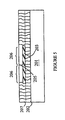
- the present invention depends on having a starting material that has a substantially defect free region prior to the deposition on the SiO 2 mask. The manner in which such a starting material is generated may be more easily understood with reference to Figure 5 which is a cross-sectional view of a GaN layer grown on a sapphire substrate 201.
- the GaN layer is started by epitaxially growing a layer of GaN 202 on the sapphire substrate.
- such a layer has a high density of dislocations resulting from the lattice mis-match between GaN and sapphire.
- GaN grown directly on sapphire In certain cases, AlN or GaN buffer layers are grown prior to bulk GaN growth. The buffer layers are for nucleation purposes.
- a layer having fewer dislocations is generated by depositing a SiO 2 strip 203 on layer 202 and then epitaxially growing an additional layer 207 of GaN over the strip.
- the GaN that extends over the SiO 2 strip is essentially defect free. There is, however, a large defect over the strip at the location at which the GaN growth from each side of the strip meets. Such a defect is shown at 205. However, the regions 206 between this defect and the edge of the SiO 2 strip are substantially defect free or significantly lower in defect density.
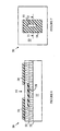
- FIG. 6-12 illustrate the construction of a laser 50 according to the present invention.
- the fabrication process begins by creating a substantially defect free region of n-GaN on which a SiO 2 mask is deposited. As noted above, this can be accomplished by growing an n-GaN layer 52 on a sapphire substrate 51 as shown in Figures 6 and 7.
- Figure 7 is a top view of laser 50
- Figure 6 is a cross-sectional view through line 71-72 shown in Figure 7.
- a SiO 2 pad 58 is then deposited on layer 52 and a second layer 53 of n-GaN grown over the pad by epitaxial growth from the portion of layer 52 to the sides of pad 58.
- a region of substantially defect free GaN forms over pad 58.
- a SiO 2 mask 54 is then deposited on the layer 53 and covers the defect 205 discussed above with reference to Figure 5.
- Mask 54 has an opening 55 which overlies the substantially defect-free region of layer 53.
- Figure 9 is a top view of the device
- Figure 8 is a cross-sectional view through line 71-72
- Figure 10 is a cross-sectional view through line 73-74 shown in Figure 9.
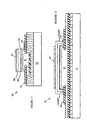
- the layers in order of growth are the n-GaN layer 61, n-type AlGaN cladding layer 63, active layer 64, a p-type AlGaN cladding layer 65 and a p-type GaN layer 66.
- the natural facets of p-GaN layer 66 provide the end mirrors for the laser's optical cavity.
- the contact 67 to the p-GaN layer shown at 66 is patterned such that the portion of active layer 64 that underlies the contact includes the vertical portions of the active layer.
- the connections to layer 61 may be made by depositing one or more contacts on the surface of layer 53 as shown at 69. It should be noted that mask 54 will constrain the current flow to the desired portion of the active layer.
- Figures 11 and 12 are cross-sectional views of laser 50, after two optional etching steps have been performed.
- Figure 11 is a view through line 71-72 shown in Figure 9
- Figure 12 is a view through line 73-74.
- the walls of the laser that are perpendicular to the mirror facets are etched to remove any extraneous current paths. Since the reflectivity of these walls does not determine gain of the laser, imperfections in the etched walls do not interfere with the laser's operation.
- the teachings of the present invention can be applied to a layer constructed from any III-V material, e.g. InP, GaAs, etc. It should also be noted that the various layers of the laser may be constructed from different III-V semiconducting materials or combinations of layers of different III-V semiconducting materials.
- the mask material is a dielectric such as SiO 2 , SiC, Si 3 N 4 , TiN AlN, etc.
- the mask material is a dielectric such as SiO 2 , SiC, Si 3 N 4 , TiN AlN, etc.
- conductors such as carbonized polymers can also be utilized provided any layers that would be shorted by the mask are separated from the mask after the layers have been deposited.
Landscapes
- Physics & Mathematics (AREA)
- Condensed Matter Physics & Semiconductors (AREA)
- General Physics & Mathematics (AREA)
- Electromagnetism (AREA)
- Optics & Photonics (AREA)
- Semiconductor Lasers (AREA)
- Led Devices (AREA)
Applications Claiming Priority (2)
| Application Number | Priority Date | Filing Date | Title |
|---|---|---|---|
| US09/140,976 US6240115B1 (en) | 1998-08-27 | 1998-08-27 | Epitaxial facet formation for laser diodes based on III-V material systems |
| US140976 | 1998-08-27 |
Publications (2)
| Publication Number | Publication Date |
|---|---|
| EP0982819A1 EP0982819A1 (en) | 2000-03-01 |
| EP0982819B1 true EP0982819B1 (en) | 2005-06-01 |
Family
ID=22493618
Family Applications (1)
| Application Number | Title | Priority Date | Filing Date |
|---|---|---|---|
| EP99112852A Expired - Lifetime EP0982819B1 (en) | 1998-08-27 | 1999-07-02 | Epitaxial facet formation for laser diodes based on III-V material systems |
Country Status (4)
| Country | Link |
|---|---|
| US (1) | US6240115B1 (ja) |
| EP (1) | EP0982819B1 (ja) |
| JP (1) | JP2000077770A (ja) |
| DE (1) | DE69925547T2 (ja) |
Families Citing this family (8)
| Publication number | Priority date | Publication date | Assignee | Title |
|---|---|---|---|---|
| US6395618B2 (en) * | 1998-07-10 | 2002-05-28 | Stmicroelectronics S.R.L. | Method for manufacturing integrated structures including removing a sacrificial region |
| JP3470623B2 (ja) | 1998-11-26 | 2003-11-25 | ソニー株式会社 | 窒化物系iii−v族化合物半導体の成長方法、半導体装置の製造方法および半導体装置 |
| TW504754B (en) | 2000-03-24 | 2002-10-01 | Sumitomo Chemical Co | Group III-V compound semiconductor and method of producing the same |
| US6627974B2 (en) * | 2000-06-19 | 2003-09-30 | Nichia Corporation | Nitride semiconductor substrate and method for manufacturing the same, and nitride semiconductor device using nitride semiconductor substrate |
| US20060284163A1 (en) * | 2005-06-15 | 2006-12-21 | Bour David P | Single ELOG growth transverse p-n junction nitride semiconductor laser |
| US20090085055A1 (en) * | 2007-09-27 | 2009-04-02 | Hui Peng | Method for Growing an Epitaxial Layer |
| US8986835B2 (en) * | 2010-04-05 | 2015-03-24 | Purdue Research Foundation | Growth process for gallium nitride porous nanorods |
| CN108352307B (zh) * | 2015-11-12 | 2022-07-05 | 胜高股份有限公司 | Iii族氮化物半导体基板的制造方法及iii族氮化物半导体基板 |
Family Cites Families (3)
| Publication number | Priority date | Publication date | Assignee | Title |
|---|---|---|---|---|
| JP3352712B2 (ja) | 1991-12-18 | 2002-12-03 | 浩 天野 | 窒化ガリウム系半導体素子及びその製造方法 |
| KR19980079320A (ko) | 1997-03-24 | 1998-11-25 | 기다오까다까시 | 고품질 쥐에이엔계층의 선택성장방법, 고품질 쥐에이엔계층 성장기판 및 고품질 쥐에이엔계층 성장기판상에 제작하는 반도체디바이스 |
| EP0874405A3 (en) | 1997-03-25 | 2004-09-15 | Mitsubishi Cable Industries, Ltd. | GaN group crystal base member having low dislocation density, use thereof and manufacturing methods thereof |
-
1998
- 1998-08-27 US US09/140,976 patent/US6240115B1/en not_active Expired - Lifetime
-
1999
- 1999-07-02 EP EP99112852A patent/EP0982819B1/en not_active Expired - Lifetime
- 1999-07-02 DE DE69925547T patent/DE69925547T2/de not_active Expired - Fee Related
- 1999-07-30 JP JP21691799A patent/JP2000077770A/ja not_active Withdrawn
Also Published As
| Publication number | Publication date |
|---|---|
| DE69925547T2 (de) | 2006-02-02 |
| DE69925547D1 (de) | 2005-07-07 |
| JP2000077770A (ja) | 2000-03-14 |
| EP0982819A1 (en) | 2000-03-01 |
| US6240115B1 (en) | 2001-05-29 |
Similar Documents
| Publication | Publication Date | Title |
|---|---|---|
| US7829900B2 (en) | Nitride-based semiconductor element and method of forming nitride-based semiconductor | |
| US6765233B2 (en) | Semiconductor substrate, light emitting device, and method for producing the same | |
| US8368183B2 (en) | Nitride semiconductor device | |
| US6829270B2 (en) | Nitride III-V compound semiconductor substrate, its manufacturing method, manufacturing method of a semiconductor light emitting device, and manufacturing method of a semiconductor device | |
| US6606335B1 (en) | Semiconductor laser, semiconductor device, and their manufacture methods | |
| KR100917260B1 (ko) | 결정막, 결정기판 및 반도체장치 | |
| US8750343B2 (en) | Nitride-based semiconductor light-emitting device, nitride-based semiconductor laser device, nitride-based semiconductor light-emitting diode, method of manufacturing the same, and method of forming nitride-based semiconductor layer | |
| JP3571641B2 (ja) | 窒化物半導体素子 | |
| US7109049B2 (en) | Method for fabricating a nitride semiconductor light-emitting device | |
| US6734503B2 (en) | Nitride-based semiconductor element | |
| EP1104031A2 (en) | Nitride semiconductor, nitride semiconductor device, semiconductor light emiting device and method of fabricating the same | |
| JP2009081374A (ja) | 半導体発光素子 | |
| US6362515B2 (en) | GaN substrate including wide low-defect region for use in semiconductor element | |
| US20240079856A1 (en) | Method of fabricating a resonant cavity and distributed bragg reflector mirrors for a vertical cavity surface emitting laser on a wing of an epitaxial lateral overgrowth region | |
| US20030047746A1 (en) | GaN substrate formed over GaN layer having discretely formed minute holes produced by use of discretely arranged growth suppression mask elements | |
| US20210381124A1 (en) | Method of obtaining a smooth surface with epitaxial lateral overgrowth | |
| EP0982819B1 (en) | Epitaxial facet formation for laser diodes based on III-V material systems | |
| KR100639747B1 (ko) | 반도체 레이저, 반도체 장치 및 이들의 제조 방법 | |
| JP4608731B2 (ja) | 半導体レーザの製造方法 | |
| JP4720051B2 (ja) | 窒化物系iii−v族化合物半導体基板およびその製造方法ならびに半導体発光素子の製造方法ならびに半導体装置の製造方法 | |
| JP3469847B2 (ja) | 窒化物系半導体素子およびその製造方法 | |
| JP2001274517A (ja) | 半導体素子用基板およびその製造方法およびその半導体素子用基板を用いた半導体素子 | |
| KR19980059917A (ko) | 청색 레이저 다이오드 | |
| JP2001274518A (ja) | 半導体素子用基板およびその製造方法およびそれを用いた半導体素子 |
Legal Events
| Date | Code | Title | Description |
|---|---|---|---|
| PUAI | Public reference made under article 153(3) epc to a published international application that has entered the european phase |
Free format text: ORIGINAL CODE: 0009012 |
|
| AK | Designated contracting states |
Kind code of ref document: A1 Designated state(s): DE FR GB |
|
| AX | Request for extension of the european patent |
Free format text: AL;LT;LV;MK;RO;SI |
|
| 17P | Request for examination filed |
Effective date: 20000619 |
|
| AKX | Designation fees paid |
Free format text: DE FR GB |
|
| RAP1 | Party data changed (applicant data changed or rights of an application transferred) |
Owner name: AGILENT TECHNOLOGIES, INC. |
|
| RAP1 | Party data changed (applicant data changed or rights of an application transferred) |
Owner name: AGILENT TECHNOLOGIES INC. |
|
| RAP1 | Party data changed (applicant data changed or rights of an application transferred) |
Owner name: AGILENT TECHNOLOGIES INC. A DELAWARE CORPORATION |
|
| RAP1 | Party data changed (applicant data changed or rights of an application transferred) |
Owner name: AGILENT TECHNOLOGIES, INC. (A DELAWARE CORPORATION |
|
| 17Q | First examination report despatched |
Effective date: 20040302 |
|
| GRAP | Despatch of communication of intention to grant a patent |
Free format text: ORIGINAL CODE: EPIDOSNIGR1 |
|
| GRAS | Grant fee paid |
Free format text: ORIGINAL CODE: EPIDOSNIGR3 |
|
| GRAA | (expected) grant |
Free format text: ORIGINAL CODE: 0009210 |
|
| AK | Designated contracting states |
Kind code of ref document: B1 Designated state(s): DE FR GB |
|
| REG | Reference to a national code |
Ref country code: GB Ref legal event code: FG4D |
|
| REF | Corresponds to: |
Ref document number: 69925547 Country of ref document: DE Date of ref document: 20050707 Kind code of ref document: P |
|
| PG25 | Lapsed in a contracting state [announced via postgrant information from national office to epo] |
Ref country code: GB Free format text: LAPSE BECAUSE OF NON-PAYMENT OF DUE FEES Effective date: 20050901 |
|
| ET | Fr: translation filed | ||
| PLBE | No opposition filed within time limit |
Free format text: ORIGINAL CODE: 0009261 |
|
| STAA | Information on the status of an ep patent application or granted ep patent |
Free format text: STATUS: NO OPPOSITION FILED WITHIN TIME LIMIT |
|
| 26N | No opposition filed |
Effective date: 20060302 |
|
| GBPC | Gb: european patent ceased through non-payment of renewal fee |
Effective date: 20050901 |
|
| PGFP | Annual fee paid to national office [announced via postgrant information from national office to epo] |
Ref country code: FR Payment date: 20060717 Year of fee payment: 8 |
|
| PGFP | Annual fee paid to national office [announced via postgrant information from national office to epo] |
Ref country code: DE Payment date: 20070628 Year of fee payment: 9 |
|
| REG | Reference to a national code |
Ref country code: FR Ref legal event code: ST Effective date: 20080331 |
|
| PG25 | Lapsed in a contracting state [announced via postgrant information from national office to epo] |
Ref country code: FR Free format text: LAPSE BECAUSE OF NON-PAYMENT OF DUE FEES Effective date: 20070731 |
|
| PG25 | Lapsed in a contracting state [announced via postgrant information from national office to epo] |
Ref country code: DE Free format text: LAPSE BECAUSE OF NON-PAYMENT OF DUE FEES Effective date: 20090203 |