EP0977253A2 - Flipchip-Verbindung von Halbleiterchips - Google Patents
Flipchip-Verbindung von Halbleiterchips Download PDFInfo
- Publication number
- EP0977253A2 EP0977253A2 EP99201355A EP99201355A EP0977253A2 EP 0977253 A2 EP0977253 A2 EP 0977253A2 EP 99201355 A EP99201355 A EP 99201355A EP 99201355 A EP99201355 A EP 99201355A EP 0977253 A2 EP0977253 A2 EP 0977253A2
- Authority
- EP
- European Patent Office
- Prior art keywords
- assembly
- semiconductor
- contact pads
- temperature
- substrate
- Prior art date
- Legal status (The legal status is an assumption and is not a legal conclusion. Google has not performed a legal analysis and makes no representation as to the accuracy of the status listed.)
- Granted
Links
Images

Classifications
-
- H—ELECTRICITY
- H10—SEMICONDUCTOR DEVICES; ELECTRIC SOLID-STATE DEVICES NOT OTHERWISE PROVIDED FOR
- H10W—GENERIC PACKAGES, INTERCONNECTIONS, CONNECTORS OR OTHER CONSTRUCTIONAL DETAILS OF DEVICES COVERED BY CLASS H10
- H10W72/00—Interconnections or connectors in packages
- H10W72/01—Manufacture or treatment
- H10W72/011—Apparatus therefor
- H10W72/0113—Apparatus for manufacturing die-attach connectors
-
- H—ELECTRICITY
- H10—SEMICONDUCTOR DEVICES; ELECTRIC SOLID-STATE DEVICES NOT OTHERWISE PROVIDED FOR
- H10W—GENERIC PACKAGES, INTERCONNECTIONS, CONNECTORS OR OTHER CONSTRUCTIONAL DETAILS OF DEVICES COVERED BY CLASS H10
- H10W70/00—Package substrates; Interposers; Redistribution layers [RDL]
- H10W70/40—Leadframes
-
- H—ELECTRICITY
- H10—SEMICONDUCTOR DEVICES; ELECTRIC SOLID-STATE DEVICES NOT OTHERWISE PROVIDED FOR
- H10W—GENERIC PACKAGES, INTERCONNECTIONS, CONNECTORS OR OTHER CONSTRUCTIONAL DETAILS OF DEVICES COVERED BY CLASS H10
- H10W72/00—Interconnections or connectors in packages
- H10W72/01—Manufacture or treatment
- H10W72/0198—Manufacture or treatment batch processes
-
- H—ELECTRICITY
- H10—SEMICONDUCTOR DEVICES; ELECTRIC SOLID-STATE DEVICES NOT OTHERWISE PROVIDED FOR
- H10W—GENERIC PACKAGES, INTERCONNECTIONS, CONNECTORS OR OTHER CONSTRUCTIONAL DETAILS OF DEVICES COVERED BY CLASS H10
- H10W72/00—Interconnections or connectors in packages
- H10W72/071—Connecting or disconnecting
- H10W72/0711—Apparatus therefor
-
- H—ELECTRICITY
- H10—SEMICONDUCTOR DEVICES; ELECTRIC SOLID-STATE DEVICES NOT OTHERWISE PROVIDED FOR
- H10W—GENERIC PACKAGES, INTERCONNECTIONS, CONNECTORS OR OTHER CONSTRUCTIONAL DETAILS OF DEVICES COVERED BY CLASS H10
- H10W72/00—Interconnections or connectors in packages
- H10W72/30—Die-attach connectors
-
- H—ELECTRICITY
- H10—SEMICONDUCTOR DEVICES; ELECTRIC SOLID-STATE DEVICES NOT OTHERWISE PROVIDED FOR
- H10W—GENERIC PACKAGES, INTERCONNECTIONS, CONNECTORS OR OTHER CONSTRUCTIONAL DETAILS OF DEVICES COVERED BY CLASS H10
- H10W74/00—Encapsulations, e.g. protective coatings
- H10W74/01—Manufacture or treatment
- H10W74/012—Manufacture or treatment of encapsulations on active surfaces of flip-chip devices, e.g. forming underfills
-
- H—ELECTRICITY
- H10—SEMICONDUCTOR DEVICES; ELECTRIC SOLID-STATE DEVICES NOT OTHERWISE PROVIDED FOR
- H10W—GENERIC PACKAGES, INTERCONNECTIONS, CONNECTORS OR OTHER CONSTRUCTIONAL DETAILS OF DEVICES COVERED BY CLASS H10
- H10W74/00—Encapsulations, e.g. protective coatings
- H10W74/10—Encapsulations, e.g. protective coatings characterised by their shape or disposition
- H10W74/15—Encapsulations, e.g. protective coatings characterised by their shape or disposition on active surfaces of flip-chip devices, e.g. underfills
-
- H—ELECTRICITY
- H10—SEMICONDUCTOR DEVICES; ELECTRIC SOLID-STATE DEVICES NOT OTHERWISE PROVIDED FOR
- H10W—GENERIC PACKAGES, INTERCONNECTIONS, CONNECTORS OR OTHER CONSTRUCTIONAL DETAILS OF DEVICES COVERED BY CLASS H10
- H10W72/00—Interconnections or connectors in packages
- H10W72/071—Connecting or disconnecting
- H10W72/072—Connecting or disconnecting of bump connectors
-
- H—ELECTRICITY
- H10—SEMICONDUCTOR DEVICES; ELECTRIC SOLID-STATE DEVICES NOT OTHERWISE PROVIDED FOR
- H10W—GENERIC PACKAGES, INTERCONNECTIONS, CONNECTORS OR OTHER CONSTRUCTIONAL DETAILS OF DEVICES COVERED BY CLASS H10
- H10W72/00—Interconnections or connectors in packages
- H10W72/071—Connecting or disconnecting
- H10W72/073—Connecting or disconnecting of die-attach connectors
-
- H—ELECTRICITY
- H10—SEMICONDUCTOR DEVICES; ELECTRIC SOLID-STATE DEVICES NOT OTHERWISE PROVIDED FOR
- H10W—GENERIC PACKAGES, INTERCONNECTIONS, CONNECTORS OR OTHER CONSTRUCTIONAL DETAILS OF DEVICES COVERED BY CLASS H10
- H10W72/00—Interconnections or connectors in packages
- H10W72/851—Dispositions of multiple connectors or interconnections
- H10W72/853—On the same surface
- H10W72/856—Bump connectors and die-attach connectors
-
- H—ELECTRICITY
- H10—SEMICONDUCTOR DEVICES; ELECTRIC SOLID-STATE DEVICES NOT OTHERWISE PROVIDED FOR
- H10W—GENERIC PACKAGES, INTERCONNECTIONS, CONNECTORS OR OTHER CONSTRUCTIONAL DETAILS OF DEVICES COVERED BY CLASS H10
- H10W72/00—Interconnections or connectors in packages
- H10W72/90—Bond pads, in general
- H10W72/921—Structures or relative sizes of bond pads
- H10W72/923—Bond pads having multiple stacked layers
-
- H—ELECTRICITY
- H10—SEMICONDUCTOR DEVICES; ELECTRIC SOLID-STATE DEVICES NOT OTHERWISE PROVIDED FOR
- H10W—GENERIC PACKAGES, INTERCONNECTIONS, CONNECTORS OR OTHER CONSTRUCTIONAL DETAILS OF DEVICES COVERED BY CLASS H10
- H10W72/00—Interconnections or connectors in packages
- H10W72/90—Bond pads, in general
- H10W72/941—Dispositions of bond pads
- H10W72/9415—Dispositions of bond pads relative to the surface, e.g. recessed, protruding
-
- H—ELECTRICITY
- H10—SEMICONDUCTOR DEVICES; ELECTRIC SOLID-STATE DEVICES NOT OTHERWISE PROVIDED FOR
- H10W—GENERIC PACKAGES, INTERCONNECTIONS, CONNECTORS OR OTHER CONSTRUCTIONAL DETAILS OF DEVICES COVERED BY CLASS H10
- H10W72/00—Interconnections or connectors in packages
- H10W72/90—Bond pads, in general
- H10W72/951—Materials of bond pads
- H10W72/952—Materials of bond pads comprising metals or metalloids, e.g. PbSn, Ag or Cu
-
- H—ELECTRICITY
- H10—SEMICONDUCTOR DEVICES; ELECTRIC SOLID-STATE DEVICES NOT OTHERWISE PROVIDED FOR
- H10W—GENERIC PACKAGES, INTERCONNECTIONS, CONNECTORS OR OTHER CONSTRUCTIONAL DETAILS OF DEVICES COVERED BY CLASS H10
- H10W90/00—Package configurations
- H10W90/701—Package configurations characterised by the relative positions of pads or connectors relative to package parts
- H10W90/721—Package configurations characterised by the relative positions of pads or connectors relative to package parts of bump connectors
- H10W90/724—Package configurations characterised by the relative positions of pads or connectors relative to package parts of bump connectors between a chip and a stacked insulating package substrate, interposer or RDL
-
- H—ELECTRICITY
- H10—SEMICONDUCTOR DEVICES; ELECTRIC SOLID-STATE DEVICES NOT OTHERWISE PROVIDED FOR
- H10W—GENERIC PACKAGES, INTERCONNECTIONS, CONNECTORS OR OTHER CONSTRUCTIONAL DETAILS OF DEVICES COVERED BY CLASS H10
- H10W90/00—Package configurations
- H10W90/701—Package configurations characterised by the relative positions of pads or connectors relative to package parts
- H10W90/731—Package configurations characterised by the relative positions of pads or connectors relative to package parts of die-attach connectors
- H10W90/734—Package configurations characterised by the relative positions of pads or connectors relative to package parts of die-attach connectors between a chip and a stacked insulating package substrate, interposer or RDL
Definitions
- the present invention relates in general to the field of integrated circuit assembly and more specifically to methods of reducing mechanical stresses when semiconductor chips having dielectric layers of low dielectric constants are flip-chip assembled onto substrates.
- CTE coefficient of thermal expansion
- the gap is customarily filled with a polymeric material which encapsulates the bumps and fills any space in the gap between the semiconductor chip and the substrate.
- a polymeric material which encapsulates the bumps and fills any space in the gap between the semiconductor chip and the substrate.
- the encapsulant is typically applied after the solder bumps are reflowed to bond the integrated circuit chip to the printed circuit substrate.
- a polymeric precursor sometimes referred to as the "underfill” is dispensed onto the substrate adjacent to the chip and is pulled into the gap by capillary forces.
- the precursor is the heated, polymerized and "cured” to form the encapsulant. It is well known in the industry that the elevated temperature and the temperature cycling needed for this curing can also create mechanical stresses which can be detrimental to the chip and the solder interconnections. The stresses may delaminate the solder joint, crack the passivation of the chip, or propagate fractures into the circuit structures. In general, the sensitivity to cracking of the layered strucutres of integrated circuits is increasing strongly with decreasing thicknesses of the various layers.
- the frame During curing and later during thermal cycling, the frame provides enhanced mechanical strength by locally constraining the substrate and the encapsulant to reduce the effect of stresses, and the frame is affixed to the substrate so that the frame becomes an integral part of the substrate.
- the proposal is expensive and does not prevent the stresses appearing in the first place.
- the present teachings comprise semiconductor ball-grid array packages, chip-size packages and flip-chip assemblies with improved mechanical reliability achieved by dramatically reduced stress during fabrication.
- the teachings are particularly important for all semiconductor products employing thin insulating layers with low dielectric constants and high mechanical brittleness, often in a multi-level architecture.
- the teachings define the process rules for solder attachment and underfill and the methods for fabricating the chip/substrate assemblies without cracking the thin dielectric layers.
- CTE coefficients of thermal expansion
- silicon has approximately 2.3, various metals from 4.3 to 17.0, and various plastics from 16.0 to 25.0. Consequently, whenever these assemblies undergo temperature excursions, the swings of increasing and decreasing temperatures induce different expansions and contractions in the materials coupled to each other, causing tensile and compressive stresses to build up in the component parts.
- the stresses in each individual layer could be analytically modeled. However, the package is not a uniform laminate, and the variations from the uniform laminate case create stress concentrations. Further, the package is assembled through a series of thermal process steps which build in stresses between various layers. Finite element analysis and measurements by test structures have proven indispensable in quantifying these stresses and locating strain and stress maxima.
- the pressure of a flowing medium is smaller the greater its velocity. Consequently, the pressure at the smaller cross sections is smaller than at the larger cross sections.
- the pressure drop of the medium along the tube length is directly proportional to the first power of the average velocity and inverse proportional to the second power of the tube radius.
- the pressure drop of the medium along the tube length is directly proportional to the second power of the average velocity and inverse proportional to the first power of the tube radius.
- the invention includes equipment for dispensing deformable medium under the requirement to dispense, per unit of time, equal amounts of deformable medium at the outlets of all distribution tubes. Since the distribution tubes are connected by different lengths of header, the pressure drop along these lengths have to be compensated by modifying the cross section of each outlet ("nozzle") such that equal amounts of deformable medium per unit time will exit through the nozzles. Practical solutions are complex due to the relatively high viscosity of the deformable medium to be used, and the fact that the medium is a mixture of plastic precursor and finely dispersed but concentrated solid fillers. Important design features of the equipment are obtained graphically, with the flowing characteristics of the medium (polymeric precursor, fillers, temperature, viscosity) as parameter. For distribution nozzles at repetitive distances ("pitch"), the whole-number multiples of the edge outline of the chips-on-substrates to be assembled serves as another parameter.
- Another object of the present teachings is to provide equipment design and process methods which are flexible so that they can be applied to several families of products, and are general, so that they can be applied to several future generations of products.
- Another object of the present teachings is to provide a low-cost and high speed process for fabrication and assembly.
- Another object of the present teachings is to minimize the cost of capital investment and to use the installed fabrication equipment base.
- a method of temperature variation in underfill processes is provided, based on finite element analysis, to reduce stress in dielectric layers of the chips and in solder ball joints of the assemblies to values safe for operating the assembly.
- Another disclosed embodiment comprises an apparatus for temperature control and temperature measurement, suitable for practising the fabrication method of the present teachings to mass produce stress-reduced assemblies.
- Another disclosed embodiment comprises an apparatus for multiple controlled dispensing of a deformable medium.
- the dispense rate of an apparatus for multiple controlled dispensing is correlated with the distance of the nozzles from the center feed tube and the cross section of the nozzle, so that a desirable dispense rate can be produced, for instance a rate which is equal for all nozzles.
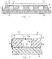
- An integrated circuit chip 10 preferably formed of silicon, comprises an active surface 11 and an inactive surface 12 which are planar and parallel to each other.
- Chip 10 is mounted to a substrate 14, integral with interconnections and a plurality of contact pads 15, yet spaced apart by a gap 16.
- Substrate 14 preferably comprises a printed circuit board made of FR-4 or a glass-epoxy laminate; contact pads 15 are preferably composed of solder-wettable copper. Chip 10 is attached by solder bumps interconnections 17 which extend across the gap and connect the contact pads 13 on the chip to the contact pads 15 on the substrate both electrically and mechanically.
- solder bumps interconnections 17 which extend across the gap and connect the contact pads 13 on the chip to the contact pads 15 on the substrate both electrically and mechanically.
- a lead-tin alloy of a desirable melting temperature is chosen for solder bumps 17 to accomplish the solder reflow at a practical temperature.
- the protective overcoat 19 in FIGS. 1 and 2 is preferably made of silicon nitride with a typical thickness in the range from 800 to 1200 nm.
- the dielectric layers used in the multi-level metal hierarchies are preferably made of insulators with low dielectric constants.
- Examples for these dielectric layers are hydrogen silsesquioxane-based (HSQ) spun-on glass; or a sandwich structures of a first film formed of plasma-generated tetraethylorthosilicate (TEOS) oxide, followed by a second film formed of inorganic porous, low density HSQ silicon oxides, followed by a third film formed of plasma-generated TEOS oxide; or methylsiloxane-based spun-on glass.
- the thickness of a typical sandwich preferably ranges from 300 to 700 nm.
- Another option is a layer made of organic materials. The goal is in every case to generate dielectric layers with a dielectric constant between about 4.0 and 3.0.
- the gap 16 is filled with a polymeric encapsulant 18 that extends over the printed circuit board about the perimeter of the chip.
- the main purpose of encapsulant 18, commonly referred to as the "underfill” material, is a reduction of mechanical stress in the assembly; another purpose is the protection of the active chip surface. To appreciate the inadequacy of the known technology related to the underfill and the importance of the present teachings, the origin of the mechanical stress has to be investigated.
- Silicon the preferred semiconductor material of chip 10
- the materials are mechanically coupled intimately, even rigidly, to each other in the assembly of a ball-grid array package.
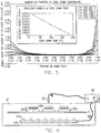
- the temperature profile is plotted as function of assembly time in FIG. 3, with temperature measured in °C, time in minutes.
- stress in arbitrary units
- the reflow of the solder bumps follows the temperature profile indicated by graph section 30, while the corresponding stress profile is plotted by graph section 31.
- the temperature reaches the maximum of 220 °C (reference number 30a) because of an overshoot over the melting temperature of 183 °C of the eutectic tin-lead alloy ( 63 weight % tin).
- the stress is zero, as indicated by reference point 31a, and stays zero to the eutectic temperature of 183 °C. With continued cooling of the assembly, though, stress starts appearing (31b) and increases rapidly.
- the stress levels reach levels so high (31c) that damage by cracking has been inflicted to the structurally weakest parts of the assembly, especially the solder joints, the chip multilevel dielectric films, or the protective overcoat film 19 in FIGS. 1 and 2.
- the integrated circuit chip 10 in FIGS. 1 and 2 is now arranged on substrate 14 such that each of the substrate contact pads 15 registers with a chip contact pad 13, with the solder bumps therebetween.
- the gap 16 between active surface 11 of the chip and the substrate is preferably between 25 and 150 ⁇ m.
- the next step is renewed heating of the assembly in order to underfill the polymeric precursor 18 into the gap 16.
- the assembly is moved to the underfill work station and the temperature is increased to 75 to 90 °C (reference number 32 in FIG. 3) in order to lower the viscosity of the plastic precursor.
- the standard dispensing procedure using a syringe with a single nozzle will be described in FIG. 7.
- one or more drops of the polymeric precursor are dispensed onto the substrate 14 adjacent to the perimeter of chip 10.
- the presursor is then drawn into gap 16 by capillary forces until it completely fills gap 16 from the chip surface to the substrate and surrounding the solder balls, leaving no void which would initiate additional failure mechanisms.
- the stress in the assembly drops, as indicated by the decline of the stress data in FIG. 3 from 31c to 33a.
- the stress increases again to values (33b) as high as in the previous cooling cycle (31c).
- the temperature is raised again (34), between about 120 to 180 °C, in order to polymerize, or "cure", the polymeric precursor.
- the assembly with the finished encapsulant is slowly brought back to room temperature (36).
- the stress values are small again (35), but increase one more time during the cooldown period. They remain at acceptable low-to-intermediate levels (37), due to the encapsulant characteristic of distributing and absorbing stress.
- the resulting encapsulant typically exhibits a CTE between about 18 and 30 ppm/°C, approximately an order magnitude higher than the CTE of the silicon chip.
- FIG. 4 shows the new temperature-time and stress-time diagram of the new assembly process flow.
- the melting temperature of 183 °C for the eutectic lead-tin mixture is overshot to about 220 °C (for about 60 to 120 s, as indicated by reference number 40a in FIG. 4).
- the stress curve 41 indicates stress level zero, 41a , and remains at zero level 41a to the eutectic melting temperature of 183 °C.
- the solder solidifies, but the assembly is kept at an elevated temperature between 80 and 140 °C, preferably between 90 and 100 °C (in FIG. 4, reference number 40b).
- the stress increases slightly from its zero level 41a to a non-critical value 41b, well below any level which could pose a risk to structurally weak dielectric layers of the chip or the solder joints.
- the height of the solidified solder bumps is preferably between 25 and 150 ⁇ , often approximately 100 ⁇ m.
- the assembly not be allowed to continue the cooling process down to room temperature, but is maintained at a constant elevated temperature (42 in FIG. 4) throughout the underfill period, which lasts about 20 min.
- the apparatus according to the present teachings is described below in FIG. 6, the equipment for the underfilling process is described in FIGS. 8, 9 and 10.
- the polymeric presursor is dispensed onto substrate 14 adjacent to the perimeter of chip 10.
- the polymeric precursor is formed of a material curable by thermal or radiation energy, preferably composed of an anhydride-hardened prepolymer such as an epoxy resin. It usually contains a catalyst such as an amine compound, and fillers such as silica (or alumina). A suitable material is supplied by the Dexter Hysol Corporation under brand FP 4527. During the underfilling cycle without cool down, the stress in the assembly remains at the low level 43 in FIG. 4.
- the apparatus of the present teachings avoids the need of a cool down to room temperature after the underfilling process. Rather, the assembly can remain in the same chamber and proceed directly to the increased temperature 44 needed for polymerizing ("curing") the underfill precursor. During this time span (about 60 to 120 min), the stress falls to the very low level 45 in FIG. 4. After the encapsulant is fully cured, the temperature is allowed to drop to room temperature 46 in the cool down period, while the stress increases only slightly to values 47, well below any risk for damage to structurally weak dielectric films or solder joints. As intended, the stress throughout the assembly is approximately uniformly distributed and for the most past absorbed by the encapsulant.
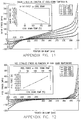
- a solder ball, or bump, of 0.1 mm height, or diameter, in worst position in a corner of the chip-substrate assembly has been selected for finite element analysis.
- the worst position has been identified earlier by failure analysis of units with cracked solder joints, or cracked dielectric or protective insulator layers.
- the magnitude of shear stress and peel (tensile) stress have been analyzed as a function of their position from one point of the bump perimeter to the opposite point diagonally across.
- the stresses are plotted in dependence on the cooling temperature (220 to 20 °C compared to 220 to 180 °C, with several options in between).
- the graphs for shear stress are reproduced in FIG. 11, the graphs for peel (tensile) stress in FIG. 12.
- FIG. 5 the moment (torque) with regard to the center of the bump/ball, generated by the integrated forces multiplied by the displacement across the bump interface, is analyzed in dependence on the position within the bump. Again, the worst-case solder ball in the corner of the package has been selected for analysis, the bump height or diameter is 0.1 mm. As can be clearly seen, the moment reaches significant values at the perimeter of the bump/ball, but can be reduced to tolerable values by keeping the end temperature of the cooling cycle to values around 100 °C.
- FIG. 6 shows schematically part of a process chamber for semiconductor ball-grid array packages and flip-chip on substrate assemblies 60a, which offers the temperature cycles and controls required by the process depicted in FIG. 4.
- a chamber 61 with gas and humidity controlled atmosphere can place a multitude (up to several hundred) of units simultaneously over a series of tungsten halogen lamps 62a. Radiant heat is applied from the back of the substrates 60b. The radiant energy may be applied using the lamps alone, or using reflectors 62b to enhance the efficiency.
- the tungsten halogen lamps are of the type described in patent application Serial No. 08/743,691, filed 11-6-96, which is a continuation of Serial No.
- radiant energy sources as opposed to furnaces, allows rapid temperature ramping or profiling, and also more uniform and more easily controllable heating and cooling cycles. Radiant heating allows a smooth transition from ambient temperature to the desired hot temperature, and rapid thermal response.
- the radiant energy is preferably provided by an optical heat source emitting near infrared light, such as incandescent lamps (halogen lamps with tungsten filament and xenon filling).
- silicon has been found to absorb rapidly near-infrared light, which is light having a wavelength of 0.8 to about 2.8 ⁇ m.
- selected reflective surfaces do not absorb near-infrared light, so that the heating can be restricted to the packages themselves; by using selected reflective surfaces on the carrier or other non-active areas exposed to the light, the packages can be heated while the remainder of the surfaces stay at a much lower temperature. Consequently, the packages rapidly heat up to a temperature at which the solder balls 60c begin to melt and reflow (typically 183 °C).
- the heating and precursor dispensing steps are performed in a single apparatus and in a single operation without moving and without the risk of losing any alignment or suffering particulate contamination, as could easily occur in a conventional chain furnace heating operation.
- the solder reflow step is followed and is combined with the underfilling step, and does not just represent the heating of preassembled parts.
- a closed-loop temperature control strategy is employed to control the temperature profile of the chips-under-assembly.
- the package temperature is changed by changing the voltage across the lamps, since the amount of heat produced by the lamps is proportional to its voltage.
- Non-contact or contact style thermocouples or pyrometers 63 monitor the real time/temperature of the assemblies and feed the information back to temperature controller 64 which modifies the voltage across the lamps with respect to some mathematical function of the difference between the actual package temperature and the predetermined desired package temperature.
- the heating and cooling steps may be performed, for example, in an inert gas environment, such as dry nitrogen or filtered gases, to provide for additional process control and to prevent particulates from settling on the device surfaces.
- the reflector assemblies (reference number 62b in FIG. 6) are constructed to be especially low mass, utilizing a light-weight rigid skeleton with a thin sheet metal reflector surface.
- the interior of the reflective surfaces are highly polished aluminum (high relectivity and low absorption in the wavelength range used).
- the exterior surfaces of the reflective components are treated for high temperature-compatible dark surfaces, increasing emissivity and re-radiation from the exterior surfaces, hence faster cooling capability of the reflector assembly.
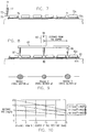
- a plurality of chips 70a with solder balls 70b and substrates 71 are placed on a support, as schematically illustrated in FIG. 7.
- a syringe 72 with a single nozzle 73 is placed adjacent to the perimeter of chip 70a.
- the polymeric precursor 74 is dispensed under slight pressure so that a drop 75 is formed at th nozzle. After separation of the drop, a bead is applied along the chip perimeter.
- the precursor With the substrate 71 preheated as described above, the precursor is drawn into the gap between chip 70a and substrate 71 by capillary forces. One or more drops of polymeric precursor will thus form fillet 76 for the assembly. Thereafter, capillary 72 is moved over to the next chip and substrate in order to produce the next assembly. The whole process consumes much time and is hard to control.
- a controllably heatable support 80 can receive and hold a multitude of substrates 81.
- Each substrate is made of electrically insulating material and has a plurality of interconnecting wiring strips and a pattern of metal contact pads.
- a semiconductor integrated circuit chip 82a such as a digital signal processor, a microprocessor, an analog device, a logic device, or a memory device.
- Each chip 82a has a pattern of metal contact pads mirror-imaging the pattern of the contact pads on the substrates 81, and one solder ball 82b attached to each contact pad. Chips 82a with solder balls 82b are aligned to the respective substrates such that the solder balls are positioned on the respective substrate contact pads.
- Thermal energy is supplied to and later withdrawn from the chips and substrates using the equipment and controls described in FIG. 6 in order to achieve the temperature-time profile described in FIG. 4.
- solder balls 82b When the solder balls 82b have reached their melting temperature (183 °C for eutectic lead-tin mixtures), their reflow is controlled so that their resulting height defines a gap spacing chip and substrate apart (for instance, 0.1 mm).
- the assembly is cooled according to the process described in FIG. 4 so that the solder soldifies, but the assembly remains at a temperature between 90 and 130 °C.
- a preferred temperature is approximately 100 °C. At this temperature, mechanical stress in the assembly remains at low values (see FIG. 5), well below any risk for introducing cracks in weak structures such as solder joints and dielectric films.
- FIG. 8 An apparatus for multiple controlled dispensing of polymeric precursor is moved over the assembly as shown in FIG. 8.
- This apparatus consists of a center feed tube 83, through which the polymeric precursor or any other reformable medium 84 is supplied under slight pressure.
- a header 85 is connected to the center feed tube 83 and a plurality of distribution tubes 86.
- FIG. 8 shows an example of three distribution tubes, but any number can be arranged.
- Each distribution tube 86 acquires a predetermined well-defined distance from the center of feed tube 83.
- At the end of each distribution tube 86 is a nozzle 87.
- each nozzle 87 is correlated to the distance of the respective distribution tube 86 from the center line of the center feed tube 83.
- the nozzles have increasingly larger cross sections, the farther the respective distribution tube is positioned from the center tube.
- FIG. 9 is schematically illustrated in FIG. 9 for the three distribution tubes of FIG. 8.
- the dispense rate of the polymeric precursor or any other deformable medium 84 can be kept the same for all distribution tubes.
- FIG. 10 shows the desired dispense rate, measured in milligrams per second (mg/s) as a function of the distance of a specific distribution tube from the center of the feed tube, measured in millimeters (mm).
- the parameter of the set of graphs in FIG. 10 is the nozzle cross section, measured in square millimeters (mm 2 ).
- the multiple-nozzle dispensing equipment such that the distribution nozzles are positioned in the repetitive distances ("pitch") of the chips-on-substrates aligned in a row for underfilling.
- An example is shown in FIG. 8 where the distribution nozzles are positioned so that every other chip can be served in one dispensing operation.
- the dispensing equipment is advanced in lockstep with the pitch of the aligned product, and the next group can be underfilled. In this fashion, even large numbers of product can be assembled in short time for mass production.
- a semiconductor assembly comprising:
- a method for the fabrication of a semiconductor assembly comprising:
Landscapes
- Wire Bonding (AREA)
- Encapsulation Of And Coatings For Semiconductor Or Solid State Devices (AREA)
Applications Claiming Priority (2)
| Application Number | Priority Date | Filing Date | Title |
|---|---|---|---|
| US8444098P | 1998-05-06 | 1998-05-06 | |
| US84440P | 1998-05-06 |
Publications (3)
| Publication Number | Publication Date |
|---|---|
| EP0977253A2 true EP0977253A2 (de) | 2000-02-02 |
| EP0977253A3 EP0977253A3 (de) | 2001-01-17 |
| EP0977253B1 EP0977253B1 (de) | 2008-08-13 |
Family
ID=22184988
Family Applications (1)
| Application Number | Title | Priority Date | Filing Date |
|---|---|---|---|
| EP99201355A Expired - Lifetime EP0977253B1 (de) | 1998-05-06 | 1999-05-01 | Flipchip-Verbindung von Halbleiterchips |
Country Status (6)
| Country | Link |
|---|---|
| US (1) | US6228680B1 (de) |
| EP (1) | EP0977253B1 (de) |
| JP (1) | JPH11345836A (de) |
| KR (1) | KR100643105B1 (de) |
| DE (1) | DE69939298D1 (de) |
| TW (1) | TW415048B (de) |
Cited By (4)
| Publication number | Priority date | Publication date | Assignee | Title |
|---|---|---|---|---|
| EP1127838A3 (de) * | 2000-02-22 | 2003-04-02 | Texas Instruments Incorporated | Flip-Chip-Assemblage geschützter Mikromechanikteile |
| WO2005069430A3 (en) * | 2004-01-13 | 2005-10-13 | Raytheon Co | Circuit board assembly and method of attaching a chip to a circuit board |
| DE102006001600B3 (de) * | 2006-01-11 | 2007-08-02 | Infineon Technologies Ag | Halbleiterbauelement mit Flipchipkontakten und Verfahren zur Herstellung desselben |
| US7763975B2 (en) | 2000-02-22 | 2010-07-27 | Texas Instruments Incorporated | Flip-chip assembly of protected micromechanical devices |
Families Citing this family (24)
| Publication number | Priority date | Publication date | Assignee | Title |
|---|---|---|---|---|
| US6794743B1 (en) * | 1999-08-06 | 2004-09-21 | Texas Instruments Incorporated | Structure and method of high performance two layer ball grid array substrate |
| JP3489113B2 (ja) * | 1999-12-20 | 2004-01-19 | 関西日本電気株式会社 | 半導体装置 |
| US7058065B2 (en) * | 2000-02-08 | 2006-06-06 | Mips Tech Inc | Method and apparatus for preventing undesirable packet download with pending read/write operations in data packet processing |
| US7042887B2 (en) * | 2000-02-08 | 2006-05-09 | Mips Technologies, Inc. | Method and apparatus for non-speculative pre-fetch operation in data packet processing |
| KR100398716B1 (ko) * | 2000-06-12 | 2003-09-19 | 가부시키가이샤 히타치세이사쿠쇼 | 반도체 모듈 및 반도체 장치를 접속한 회로 기판 |
| JP3591458B2 (ja) * | 2000-12-15 | 2004-11-17 | 松下電器産業株式会社 | 半導体装置の実装構造および半導体装置 |
| US6869831B2 (en) * | 2001-09-14 | 2005-03-22 | Texas Instruments Incorporated | Adhesion by plasma conditioning of semiconductor chip surfaces |
| US20030116845A1 (en) * | 2001-12-21 | 2003-06-26 | Bojkov Christo P. | Waferlevel method for direct bumping on copper pads in integrated circuits |
| US6696757B2 (en) | 2002-06-24 | 2004-02-24 | Texas Instruments Incorporated | Contact structure for reliable metallic interconnection |
| US20040007779A1 (en) * | 2002-07-15 | 2004-01-15 | Diane Arbuthnot | Wafer-level method for fine-pitch, high aspect ratio chip interconnect |
| US6696644B1 (en) * | 2002-08-08 | 2004-02-24 | Texas Instruments Incorporated | Polymer-embedded solder bumps for reliable plastic package attachment |
| US6677522B1 (en) | 2002-09-26 | 2004-01-13 | International Business Machines Corporation | Package for electronic component |
| JP3918098B2 (ja) * | 2002-11-14 | 2007-05-23 | 株式会社村田製作所 | 回路モジュールの製造方法 |
| JP2004281491A (ja) * | 2003-03-13 | 2004-10-07 | Toshiba Corp | 半導体装置及びその製造方法 |
| US7238538B2 (en) * | 2003-09-19 | 2007-07-03 | Freitag Helmut E | Chromatographic assay device and methods |
| US6977429B2 (en) * | 2003-12-05 | 2005-12-20 | Texas Instruments Incorporated | Manufacturing system and apparatus for balanced product flow with application to low-stress underfilling of flip-chip electronic devices |
| JP3981089B2 (ja) | 2004-02-18 | 2007-09-26 | 株式会社東芝 | 半導体装置とその製造方法 |
| TWI237370B (en) * | 2004-07-30 | 2005-08-01 | Advanced Semiconductor Eng | Chip package structure and process for fabricating the same |
| US7033864B2 (en) * | 2004-09-03 | 2006-04-25 | Texas Instruments Incorporated | Grooved substrates for uniform underfilling solder ball assembled electronic devices |
| US7585693B2 (en) * | 2006-03-31 | 2009-09-08 | Intel Corporation | Method of forming a microelectronic package using control of die and substrate differential expansions and microelectronic package formed according to the method |
| US7790509B2 (en) * | 2008-06-27 | 2010-09-07 | Texas Instruments Incorporated | Method for fine-pitch, low stress flip-chip interconnect |
| DE102010003562B4 (de) * | 2010-03-31 | 2021-11-04 | Taiwan Semiconductor Manufacturing Company, Ltd. | Verfahren und Wiederaufschmelzsystem zum Verbinden eines Halbleiterchips mit einem Gehäusesubstrat |
| DE102011079835B4 (de) | 2011-07-26 | 2018-03-22 | Globalfoundries Inc. | Verfahren zur Verringerung der mechanischen Verspannung in komplexen Halbleiterbauelementen während des Chip-Substrat-Verbindens mittels eines mehrstufigen Abkühlschemas |
| CN115081388B (zh) * | 2022-06-01 | 2024-03-22 | 华南理工大学 | 一种电子元件发热强度分配优化方法 |
Family Cites Families (11)
| Publication number | Priority date | Publication date | Assignee | Title |
|---|---|---|---|---|
| JPS58191441A (ja) * | 1982-04-19 | 1983-11-08 | インタ−ナショナル ビジネス マシ−ンズ コ−ポレ−ション | ハンダ付けされた部品の応力軽減方法 |
| US4604644A (en) * | 1985-01-28 | 1986-08-05 | International Business Machines Corporation | Solder interconnection structure for joining semiconductor devices to substrates that have improved fatigue life, and process for making |
| US5656862A (en) * | 1990-03-14 | 1997-08-12 | International Business Machines Corporation | Solder interconnection structure |
| US5121190A (en) * | 1990-03-14 | 1992-06-09 | International Business Machines Corp. | Solder interconnection structure on organic substrates |
| US5371328A (en) * | 1993-08-20 | 1994-12-06 | International Business Machines Corporation | Component rework |
| US5607773A (en) * | 1994-12-20 | 1997-03-04 | Texas Instruments Incorporated | Method of forming a multilevel dielectric |
| US5659203A (en) * | 1995-06-07 | 1997-08-19 | International Business Machines Corporation | Reworkable polymer chip encapsulant |
| US7041771B1 (en) * | 1995-08-11 | 2006-05-09 | Kac Holdings, Inc. | Encapsulant with fluxing properties and method of use in flip-chip surface mount reflow soldering |
| US5821456A (en) * | 1996-05-01 | 1998-10-13 | Motorola, Inc. | Microelectronic assembly including a decomposable encapsulant, and method for forming and reworking same |
| US5919329A (en) * | 1997-10-14 | 1999-07-06 | Gore Enterprise Holdings, Inc. | Method for assembling an integrated circuit chip package having at least one semiconductor device |
| US6190940B1 (en) * | 1999-01-21 | 2001-02-20 | Lucent Technologies Inc. | Flip chip assembly of semiconductor IC chips |
-
1999
- 1999-04-09 KR KR1019990012614A patent/KR100643105B1/ko not_active Expired - Lifetime
- 1999-04-26 TW TW088106587A patent/TW415048B/zh not_active IP Right Cessation
- 1999-04-28 JP JP11121398A patent/JPH11345836A/ja not_active Abandoned
- 1999-05-01 DE DE69939298T patent/DE69939298D1/de not_active Expired - Lifetime
- 1999-05-01 US US09/303,401 patent/US6228680B1/en not_active Expired - Lifetime
- 1999-05-01 EP EP99201355A patent/EP0977253B1/de not_active Expired - Lifetime
Cited By (5)
| Publication number | Priority date | Publication date | Assignee | Title |
|---|---|---|---|---|
| EP1127838A3 (de) * | 2000-02-22 | 2003-04-02 | Texas Instruments Incorporated | Flip-Chip-Assemblage geschützter Mikromechanikteile |
| US7763975B2 (en) | 2000-02-22 | 2010-07-27 | Texas Instruments Incorporated | Flip-chip assembly of protected micromechanical devices |
| WO2005069430A3 (en) * | 2004-01-13 | 2005-10-13 | Raytheon Co | Circuit board assembly and method of attaching a chip to a circuit board |
| DE102006001600B3 (de) * | 2006-01-11 | 2007-08-02 | Infineon Technologies Ag | Halbleiterbauelement mit Flipchipkontakten und Verfahren zur Herstellung desselben |
| US7462940B2 (en) | 2006-01-11 | 2008-12-09 | Infineon Technologies Ag | Semiconductor component comprising flip chip contacts with polymer cores and method of producing the same |
Also Published As
| Publication number | Publication date |
|---|---|
| EP0977253B1 (de) | 2008-08-13 |
| DE69939298D1 (de) | 2008-09-25 |
| EP0977253A3 (de) | 2001-01-17 |
| JPH11345836A (ja) | 1999-12-14 |
| KR100643105B1 (ko) | 2006-11-13 |
| TW415048B (en) | 2000-12-11 |
| US6228680B1 (en) | 2001-05-08 |
| KR19990087907A (ko) | 1999-12-27 |
Similar Documents
| Publication | Publication Date | Title |
|---|---|---|
| US6228680B1 (en) | Low stress method and apparatus for underfilling flip-chip electronic devices | |
| EP0955669B1 (de) | Verbesserungen an, oder in bezug auf, integrierte Schaltungsanordnungen | |
| US6245583B1 (en) | Low stress method and apparatus of underfilling flip-chip electronic devices | |
| US6191952B1 (en) | Compliant surface layer for flip-chip electronic packages and method for forming same | |
| US7594644B2 (en) | Semiconductor device and method for manufacturing the same, circuit board, electronic apparatus, and semiconductor device manufacturing apparatus | |
| US6207475B1 (en) | Method for dispensing underfill and devices formed | |
| US6674172B2 (en) | Flip-chip package with underfill having low density filler | |
| US7445960B2 (en) | Adhesion by plasma conditioning of semiconductor chip | |
| US20070200234A1 (en) | Flip-Chip Device Having Underfill in Controlled Gap | |
| US6855578B2 (en) | Vibration-assisted method for underfilling flip-chip electronic devices | |
| KR20090018442A (ko) | 반도체 칩 패키지, 그 제조 방법 및 이를 포함하는 전자소자 | |
| US20110156254A1 (en) | Modified chip attach process | |
| TWI427712B (zh) | 半導體裝置中控制未填滿流的熱分析法 | |
| US6977429B2 (en) | Manufacturing system and apparatus for balanced product flow with application to low-stress underfilling of flip-chip electronic devices | |
| US20070269930A1 (en) | Methodology to control underfill fillet size, flow-out and bleed in flip chips (FC), chip scale packages (CSP) and ball grid arrays (BGA) | |
| US7306976B2 (en) | Technique for enhancing thermal and mechanical characteristics of an underfill material of a substrate/die assembly | |
| US20030202332A1 (en) | Second level packaging interconnection method with improved thermal and reliability performance | |
| CN102248240B (zh) | 用加强冷却方法在晶粒-基板焊接过程降低精密半导体装置的金属堆栈中的机械应力 | |
| CN101390217A (zh) | 在受控间隙中具有底填充的倒装芯片装置 | |
| Lee | Development of Multi Chip Modules for Extreme Environments |
Legal Events
| Date | Code | Title | Description |
|---|---|---|---|
| PUAI | Public reference made under article 153(3) epc to a published international application that has entered the european phase |
Free format text: ORIGINAL CODE: 0009012 |
|
| AK | Designated contracting states |
Kind code of ref document: A2 Designated state(s): DE FR GB IT NL |
|
| AX | Request for extension of the european patent |
Free format text: AL;LT;LV;MK;RO;SI |
|
| PUAL | Search report despatched |
Free format text: ORIGINAL CODE: 0009013 |
|
| AK | Designated contracting states |
Kind code of ref document: A3 Designated state(s): AT BE CH CY DE DK ES FI FR GB GR IE IT LI LU MC NL PT SE |
|
| AX | Request for extension of the european patent |
Free format text: AL;LT;LV;MK;RO;SI |
|
| 17P | Request for examination filed |
Effective date: 20010717 |
|
| AKX | Designation fees paid |
Free format text: DE FR GB IT NL |
|
| 17Q | First examination report despatched |
Effective date: 20061002 |
|
| GRAJ | Information related to disapproval of communication of intention to grant by the applicant or resumption of examination proceedings by the epo deleted |
Free format text: ORIGINAL CODE: EPIDOSDIGR1 |
|
| GRAP | Despatch of communication of intention to grant a patent |
Free format text: ORIGINAL CODE: EPIDOSNIGR1 |
|
| GRAS | Grant fee paid |
Free format text: ORIGINAL CODE: EPIDOSNIGR3 |
|
| GRAA | (expected) grant |
Free format text: ORIGINAL CODE: 0009210 |
|
| AK | Designated contracting states |
Kind code of ref document: B1 Designated state(s): DE FR GB IT NL |
|
| REG | Reference to a national code |
Ref country code: GB Ref legal event code: FG4D |
|
| REF | Corresponds to: |
Ref document number: 69939298 Country of ref document: DE Date of ref document: 20080925 Kind code of ref document: P |
|
| PG25 | Lapsed in a contracting state [announced via postgrant information from national office to epo] |
Ref country code: NL Free format text: LAPSE BECAUSE OF FAILURE TO SUBMIT A TRANSLATION OF THE DESCRIPTION OR TO PAY THE FEE WITHIN THE PRESCRIBED TIME-LIMIT Effective date: 20080813 |
|
| PLBE | No opposition filed within time limit |
Free format text: ORIGINAL CODE: 0009261 |
|
| STAA | Information on the status of an ep patent application or granted ep patent |
Free format text: STATUS: NO OPPOSITION FILED WITHIN TIME LIMIT |
|
| 26N | No opposition filed |
Effective date: 20090514 |
|
| PG25 | Lapsed in a contracting state [announced via postgrant information from national office to epo] |
Ref country code: IT Free format text: LAPSE BECAUSE OF FAILURE TO SUBMIT A TRANSLATION OF THE DESCRIPTION OR TO PAY THE FEE WITHIN THE PRESCRIBED TIME-LIMIT Effective date: 20080813 |
|
| PGFP | Annual fee paid to national office [announced via postgrant information from national office to epo] |
Ref country code: GB Payment date: 20140425 Year of fee payment: 16 |
|
| PGFP | Annual fee paid to national office [announced via postgrant information from national office to epo] |
Ref country code: DE Payment date: 20140602 Year of fee payment: 16 Ref country code: FR Payment date: 20140424 Year of fee payment: 16 |
|
| REG | Reference to a national code |
Ref country code: DE Ref legal event code: R119 Ref document number: 69939298 Country of ref document: DE |
|
| GBPC | Gb: european patent ceased through non-payment of renewal fee |
Effective date: 20150501 |
|
| REG | Reference to a national code |
Ref country code: FR Ref legal event code: ST Effective date: 20160129 |
|
| PG25 | Lapsed in a contracting state [announced via postgrant information from national office to epo] |
Ref country code: GB Free format text: LAPSE BECAUSE OF NON-PAYMENT OF DUE FEES Effective date: 20150501 Ref country code: DE Free format text: LAPSE BECAUSE OF NON-PAYMENT OF DUE FEES Effective date: 20151201 |
|
| PG25 | Lapsed in a contracting state [announced via postgrant information from national office to epo] |
Ref country code: FR Free format text: LAPSE BECAUSE OF NON-PAYMENT OF DUE FEES Effective date: 20150601 |