EP0977073A2 - Doppelfunktion-Eingangselektrodentruktur für multifunktionale integrierte optische Chips ("MIOCs") - Google Patents
Doppelfunktion-Eingangselektrodentruktur für multifunktionale integrierte optische Chips ("MIOCs") Download PDFInfo
- Publication number
- EP0977073A2 EP0977073A2 EP99114785A EP99114785A EP0977073A2 EP 0977073 A2 EP0977073 A2 EP 0977073A2 EP 99114785 A EP99114785 A EP 99114785A EP 99114785 A EP99114785 A EP 99114785A EP 0977073 A2 EP0977073 A2 EP 0977073A2
- Authority
- EP
- European Patent Office
- Prior art keywords
- input
- rail
- conductive
- rails
- chip
- Prior art date
- Legal status (The legal status is an assumption and is not a legal conclusion. Google has not performed a legal analysis and makes no representation as to the accuracy of the status listed.)
- Withdrawn
Links
- 230000009977 dual effect Effects 0.000 title 1
- 239000013078 crystal Substances 0.000 claims abstract description 23
- 230000003287 optical effect Effects 0.000 claims abstract description 23
- 239000004065 semiconductor Substances 0.000 claims description 14
- 229910052751 metal Inorganic materials 0.000 claims description 9
- 239000002184 metal Substances 0.000 claims description 9
- 238000012360 testing method Methods 0.000 claims description 9
- 238000013459 approach Methods 0.000 claims description 6
- 239000004020 conductor Substances 0.000 claims description 5
- 238000004519 manufacturing process Methods 0.000 claims description 5
- 230000000694 effects Effects 0.000 claims description 4
- 230000004044 response Effects 0.000 claims description 4
- 239000004593 Epoxy Substances 0.000 claims description 3
- 238000000576 coating method Methods 0.000 claims description 3
- 238000007796 conventional method Methods 0.000 claims description 3
- 239000011248 coating agent Substances 0.000 claims description 2
- 230000005669 field effect Effects 0.000 claims description 2
- 230000008878 coupling Effects 0.000 abstract description 2
- 238000010168 coupling process Methods 0.000 abstract description 2
- 238000005859 coupling reaction Methods 0.000 abstract description 2
- GQYHUHYESMUTHG-UHFFFAOYSA-N lithium niobate Chemical compound [Li+].[O-][Nb](=O)=O GQYHUHYESMUTHG-UHFFFAOYSA-N 0.000 abstract description 2
- 238000001465 metallisation Methods 0.000 abstract 1
- 238000000034 method Methods 0.000 description 13
- 239000000835 fiber Substances 0.000 description 7
- 238000000926 separation method Methods 0.000 description 7
- 229910003327 LiNbO3 Inorganic materials 0.000 description 5
- WHXSMMKQMYFTQS-UHFFFAOYSA-N Lithium Chemical compound [Li] WHXSMMKQMYFTQS-UHFFFAOYSA-N 0.000 description 5
- 230000008859 change Effects 0.000 description 5
- 229910052744 lithium Inorganic materials 0.000 description 5
- 230000008569 process Effects 0.000 description 4
- 239000000758 substrate Substances 0.000 description 4
- 229910052737 gold Inorganic materials 0.000 description 3
- 239000010931 gold Substances 0.000 description 3
- 238000012545 processing Methods 0.000 description 3
- 238000013461 design Methods 0.000 description 2
- 230000005684 electric field Effects 0.000 description 2
- PCHJSUWPFVWCPO-UHFFFAOYSA-N gold Chemical compound [Au] PCHJSUWPFVWCPO-UHFFFAOYSA-N 0.000 description 2
- 239000000463 material Substances 0.000 description 2
- 239000013307 optical fiber Substances 0.000 description 2
- 230000010287 polarization Effects 0.000 description 2
- 239000000126 substance Substances 0.000 description 2
- OKTJSMMVPCPJKN-UHFFFAOYSA-N Carbon Chemical compound [C] OKTJSMMVPCPJKN-UHFFFAOYSA-N 0.000 description 1
- RTAQQCXQSZGOHL-UHFFFAOYSA-N Titanium Chemical compound [Ti] RTAQQCXQSZGOHL-UHFFFAOYSA-N 0.000 description 1
- 238000004458 analytical method Methods 0.000 description 1
- 230000003190 augmentative effect Effects 0.000 description 1
- 238000012512 characterization method Methods 0.000 description 1
- 239000002131 composite material Substances 0.000 description 1
- 230000001419 dependent effect Effects 0.000 description 1
- 238000005137 deposition process Methods 0.000 description 1
- 230000007613 environmental effect Effects 0.000 description 1
- 238000005530 etching Methods 0.000 description 1
- 230000001747 exhibiting effect Effects 0.000 description 1
- 229910002804 graphite Inorganic materials 0.000 description 1
- 239000010439 graphite Substances 0.000 description 1
- 238000005304 joining Methods 0.000 description 1
- 238000000608 laser ablation Methods 0.000 description 1
- 238000001459 lithography Methods 0.000 description 1
- 230000007774 longterm Effects 0.000 description 1
- 230000005693 optoelectronics Effects 0.000 description 1
- 239000003973 paint Substances 0.000 description 1
- 230000009467 reduction Effects 0.000 description 1
- 239000010936 titanium Substances 0.000 description 1
- 229910052719 titanium Inorganic materials 0.000 description 1
- 238000001771 vacuum deposition Methods 0.000 description 1
- 235000012431 wafers Nutrition 0.000 description 1
Images

Classifications
-
- G—PHYSICS
- G02—OPTICS
- G02F—OPTICAL DEVICES OR ARRANGEMENTS FOR THE CONTROL OF LIGHT BY MODIFICATION OF THE OPTICAL PROPERTIES OF THE MEDIA OF THE ELEMENTS INVOLVED THEREIN; NON-LINEAR OPTICS; FREQUENCY-CHANGING OF LIGHT; OPTICAL LOGIC ELEMENTS; OPTICAL ANALOGUE/DIGITAL CONVERTERS
- G02F1/00—Devices or arrangements for the control of the intensity, colour, phase, polarisation or direction of light arriving from an independent light source, e.g. switching, gating or modulating; Non-linear optics
- G02F1/29—Devices or arrangements for the control of the intensity, colour, phase, polarisation or direction of light arriving from an independent light source, e.g. switching, gating or modulating; Non-linear optics for the control of the position or the direction of light beams, i.e. deflection
- G02F1/31—Digital deflection, i.e. optical switching
- G02F1/313—Digital deflection, i.e. optical switching in an optical waveguide structure
- G02F1/3137—Digital deflection, i.e. optical switching in an optical waveguide structure with intersecting or branching waveguides, e.g. X-switches and Y-junctions
-
- G—PHYSICS
- G02—OPTICS
- G02F—OPTICAL DEVICES OR ARRANGEMENTS FOR THE CONTROL OF LIGHT BY MODIFICATION OF THE OPTICAL PROPERTIES OF THE MEDIA OF THE ELEMENTS INVOLVED THEREIN; NON-LINEAR OPTICS; FREQUENCY-CHANGING OF LIGHT; OPTICAL LOGIC ELEMENTS; OPTICAL ANALOGUE/DIGITAL CONVERTERS
- G02F1/00—Devices or arrangements for the control of the intensity, colour, phase, polarisation or direction of light arriving from an independent light source, e.g. switching, gating or modulating; Non-linear optics
- G02F1/01—Devices or arrangements for the control of the intensity, colour, phase, polarisation or direction of light arriving from an independent light source, e.g. switching, gating or modulating; Non-linear optics for the control of the intensity, phase, polarisation or colour
- G02F1/03—Devices or arrangements for the control of the intensity, colour, phase, polarisation or direction of light arriving from an independent light source, e.g. switching, gating or modulating; Non-linear optics for the control of the intensity, phase, polarisation or colour based on ceramics or electro-optical crystals, e.g. exhibiting Pockels effect or Kerr effect
- G02F1/035—Devices or arrangements for the control of the intensity, colour, phase, polarisation or direction of light arriving from an independent light source, e.g. switching, gating or modulating; Non-linear optics for the control of the intensity, phase, polarisation or colour based on ceramics or electro-optical crystals, e.g. exhibiting Pockels effect or Kerr effect in an optical waveguide structure
-
- G—PHYSICS
- G02—OPTICS
- G02F—OPTICAL DEVICES OR ARRANGEMENTS FOR THE CONTROL OF LIGHT BY MODIFICATION OF THE OPTICAL PROPERTIES OF THE MEDIA OF THE ELEMENTS INVOLVED THEREIN; NON-LINEAR OPTICS; FREQUENCY-CHANGING OF LIGHT; OPTICAL LOGIC ELEMENTS; OPTICAL ANALOGUE/DIGITAL CONVERTERS
- G02F2203/00—Function characteristic
- G02F2203/21—Thermal instability, i.e. DC drift, of an optical modulator; Arrangements or methods for the reduction thereof
Definitions
- the invention relates to the field of integrated optics chips or devices and more particularly to the field of multifunction integrated optics chips such as those having integrated optic circuits formed on Lithium Niobiate (LiNbO 3 ) substrates.
- Integrated optics chips are designed to include waveguides and to perform functions such as "Y”, “Y-Y”, or Star splitters, or couplers, polarizer, WDM (Wavelength Division Multiplexer) and modulators. Multiple functions are incorporated on a single device eliminating losses and errors associated with individual interface optical coupling.
- the devices are fabricated in large numbers usually on three to four inch circular wafers of Lithium Niobiate (LiNbO 3 ) using conventional photomasks, vacuum deposition, chemical baths and etching techniques to form large numbers of identical components at low cost and with high reliability.
- MIOC's Multifunction Integrated Optics Chips or Circuits or Components
- middle and high accuracy FOG's fiber optic gyros
- rotation sensors that rely on the principle of Sagnac interferometers and possibly other interferometric fiber optic sensors such as hydrophones that rely on the principles of the Mach-Zehnder or Michaelson Interferometers requiring high stability.
- the device was made of Lithium Niobiate (LiNbO 3 ) and was similar in size to the dimensioned related art device shown in Figure 1.
- the hysteresis problem exhibits itself as a slight change in the power of a device as the device is first taken through a positive or negative temperature change followed by a negative or positive temperature change.
- the charge differential that develops across the face of the chip results in a charge leakage across the face of the chip.
- the time and temperature dependent effects combine to contribute to hysteresis in the transmitted power of the device and to the efficiency of the waveguides in the device to propagate light.
- Integrated optics chips such as those characterized in this application are formed using processes and steps similar to some of those found in related U.S. Patents such as U.S. Pat. No. 5,037,205 filed 09/25/89 for a "INTEGRATED OPTIC INTERFEROMETRIC FIBER GYROSCOPE MODULE AND METHOD" which issued to George A. Pavlath on August 6, 1991 which shows a birefringence modulator comprising two electrodes formed on opposite sides of the waveguide; U.S. Pat. No.
- This application is particularly directed to methods and apparatus for the reduction of errors produced in an integrated optics chips formed to function as an optical modulator as a result of temperature differences across the surface of chip due to the Pyroelectric Effect or due to rapid changes in the temperature of the chip.
- a second application having the Attorney Docket number GCD 98-21, and U.S. Serial Number 08/ formalizing provisional application having S/N 60/080,260, filed 03/31/98 for a "Low Cost High Reliability Method of Correcting Pyroelectric Errors In Integrated Optics Chips" by Ken Shafer et al filed concurrently herewith and having a common assignee is incorporated here in by reference on issue.
- This invention teaches an Integrated Optics Chip formed on Lithium Niobate, a crystal substrate haying a high electro-optic coefficient and conventional X, Y and a Z crystal axes.
- the substrate or chip has a top surface, a +Z face and a -Z face.
- An input waveguide is coupled to receive an optical signal from an input port. The waveguide couples that signal to a waveguide network.
- At least a first and a second rail are formed on the top surface of the optic chip.
- the first and second rails are positioned to closely straddle a portion of the input waveguide.
- a conductive bridge connects the first and second rails to form a conductive network and to prevent a charge differential from developing between the first and second rails.
- the network formed by the combination of the rails and the conductive bridge are floating. They are not referenced to a system potential.
- the conductive bridge is further characterized as capable of being interrupted to permit an external drive circuit to drive the first and second rails to different potentials as might be necessary for analysis or diagnostic purposes or for calibration of the component. If desired, in an alternative embodiment, the rails can be driven to the same potential such as a system reference voltage.
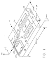
- Figure 1 provides a schematic perspective view representation of an optics chip 10 having a top surface 12, a +Z face 14 and a -Z face 16 on the opposing side.
- the chip 10 is formed from a crystal having a high electro-optic coefficient, such as Lithium Niobiate (LiNbO 3 ).
- the crystal axes are illustrated showing the +Z crystal axis extending outward, normal to the +Z face, the +X axis extending upward, normal to the top surface 12 and the +Y axis extending to the right along the longitudinal axis of the optics chip 10.
- orientation of the X - Y axes of crystal can be any crystal orientation mutually orthogonal to the +Z or -Z axis so long as the +Z or -Z axis extend outward through the +Z face 14 or the -Z face 16 of the chip and is normal to the input waveguide 18 formed in the top surface of the chip 12.
- a dimension of 20 mm along the Y axis, a width of 2 mm along the Z axis, and a thickness of 1 mm are illustrative and are only provided to show what the size might be of a typical optical chip 10.
- the optical chip 10 of Figure 1 is a MIOC that provides several functions.
- the input waveguide 18 functions as a polarizer.
- the "Y" junction 24 functions as a single 50/50 splitter.
- a first output waveguide 26 is coupled from the "Y" splitter 24 to a first output port 28 and then to a first output pigtail 29 on output face 30.
- a second output waveguide 32 is coupled from the splitter 24 to a second output port 34 and then to a second output pigtail 35 on output face 30.
- a modulator is formed by modulator plates 36a, 36b and 36c driven by electrical drive signals from modulator drive pads 37a, 37b, and 37c. respectively.
- the MIOC 10 thus formed is of a type that might be used in a conventional fiber optic gyro.
- Input waveguide 18 receives light from input port 20 on input face 22.
- the input waveguide branches at the "Y" junction 24 to a first output waveguide 26 that is coupled to a first output port 28 on output face 30 and a second output waveguide 32 coupled to a second output port 34 also on the output face 30.
- the input waveguide 18 and output waveguides 26, 32 comprise a waveguide network that functions as a polarizer. Polarization of the light into the TE mode is achieved by the proton-exchanged waveguide input waveguide 18 because a proton-exchanged waveguide presents a negative ⁇ n or change in the waveguide's index of refraction to the TM component (the vertically polarized component) of the optical signal passing through the waveguide.
- the waveguide presents a positive ⁇ n or change in the waveguide's index of refraction to a TE component (the horizontally polarized component) of the optical signal passing through the waveguide.
- the TE mode component of the signal is therefore preserved while the TM component is dissipated in the chip.
- the topology forms a "Y" splitter in combination with a phase modulator having modulator plates 36a, 36b and 36c.
- the output waveguides 26, 32 function to guide light with phase modulation and to couple the waveguide network to output ports 28, 34.
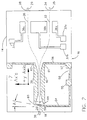
- Figure 2 is a schematic top view of the optics chip 10 viewing the top surface 12.
- the orientation of the +Z axis is substantially orthogonal to the input waveguide 18.
- Input waveguide 18 is coupled to receive an optical signal (not shown) from an input port 20 via fiber optic pigtail 39.
- the input waveguide 18 couples the optical signal to a waveguide network, which in the example of Figure 2 comprises a "Y" splitter 24 formed by the bifurcation of the input waveguide 18 into the first and second output waveguides 26, 32 respectively and the modulator electrodes or modulator plates 36a - 36c and their associated drive circuitry and pads 37a, 37b and 37c.
- Figure 2 shows the first and second rails 38, 40 positioned on the top surface of the optic chip.
- the rails straddle a portion of the input waveguide 18 and are formed on the top surface 12 from metal.
- Figure 3 is a schematic plan view of the chip expanded to show that each of the rails 38, 40 has a respective tapered input segment 42a, 42b that has input end 43a, 43b an output end 44a, 44b; a respective parallel segment 45a, 45b having an input end 46a, 46b, an output end 48a, 48b; a respective tapered output segment 49a, 49b having an input end 50a, 50b and an output end 51a, 51b.
- the rails 38, 40 are substantially of the same length by design.
- the separation between the edge of the rail and the edge of the waveguide must be maintained.
- the gap or separation is reduced as far as it is practical to do so and is limited only by present processing limitations such as the quality of the lithography, the deposition process and masks.
- the present separation is estimated to be one to five microns on each side of the input waveguide 18.
- the input waveguide is estimated to have a width of from three to seven microns.
- the gap must not be too small or excessive waveguide losses will occur.
- the separation between the parallel segments is estimated to be typically 7 - 15 um.
- the width of the waveguides and the separation between parallel segments 45a, 45b will depend on the design wavelength of the waveguide.
- An object of the invention is to provide shielding between the "Y" junction and the modulator plates 36a, 36b and 36c.
- the signal driving these plates is typically a switching wave form with an amplitude controlled to impose a predetermined phase modulation on the optical signals passing through the first and second output waveguides 26, 28.
- the electric field produced by the modulator drive signals is sufficient to produce amplitude modulation on the optical signals entering and leaving the initial entry point to the "Y" junction. Absent adequate shielding, the amplitude modulation produced at the "Y" junction by the electric field of the modulation drive signal on the same chip is sufficient to impose a substantial burden on the processing electronics that receives and processes the detected output signal of a FOG.
- the signals passing through the "Y" junction are therefore shielded in the preferred embodiment of Figures 2 and 3 from the fields of the modulation drive signals by extending the output ends 51a, 51b of the tapered output segments 49a, 49b past the "Y" junction along the diverging waveguides 26, 32.
- the extension of the rails is carried past a point at which the waveguides are separated by a distance that exceeds five times the width of the input waveguide 18.
- the gap between each rail and its respective output waveguide 26, 32 is maintained at three to five microns to output ends 51a, 51b of the output segments 49a, 49b.
- FIG 3 shows that each respective tapered input segment 42a, 42b has an input end 43a, 43b proximate or close to the input port 20, i.e. toward the left end of Figure 3, and separated from the input waveguide 18 by a distance orthogonal to the input waveguide sufficient to minimize loss or reflections.
- Separation “B” shown on Figure 2 depicts the separation between the respective input ends of the tapered input segments from the input waveguide 18.
- output ends 44a, 44b lead to the input ends 46a, 46b of the parallel segment 45a, 45b. They are formed and positioned on the surface of the optics chip to adiabatically, or tangentially approach the input ends 46a, 46b of the parallel segment 45a, 45b straddling the input waveguide 18.
- the output end 44a, 44b of each respective tapered input segment 42a, 42b homogeneously merges tangentially with the input end 46a, 46b of the corresponding parallel segment 45a, 45b.
- adiabatic is meant to convey the concept of defining the curve of the input and output segments of the rails to be so gradual when joining the parallel segment as to avoid disturbing the signal passing through the input waveguide as possible. It should be understood that the characterization of the tapered input and output segments in the Figures is an example only.
- a conductive bridge 52 comprises a first rail conductive segment 54, a first bonding pad 55, a second rail conductive segment 56 and a second bonding pad 57.
- the first and second bonding pads 55, 57 are connected by conductive jumper bridge 58.
- a conductive crossing segment 59 is shown as a first portion of the first rail conductive segment 54.
- Figure 3 shows that the input end 43a, 43b of at least one input segment 42a, 42b is coupled to a first end of a conductive crossing segment 58.
- the conductive crossing segment 58 is very thin and is characterized to cross or traverse the input waveguide 18 at an angle "A" selected to cause minimum reflections or losses in signal passing through the input waveguide 18.
- each respective tapered output segment 42a, 42b has an input end 50a, 50b coupled to the respective output end 48a, 48b of the respective parallel segment 45a, 45b.
- the tapered output segments 49a, 49b curve away from the parallel segment 45a, 45b and the "Y" junction 24 in an adiabatic manner to avoid reflections and to diminish losses.
- the first rail 38 is connected to a first bonding pad 55 via a first rail conductive segment 54.
- the second rail 40 is connected to a second bonding pad 57 via a second rail conductive segment 56.
- a conductive jumper bridge 58 connects the first and second rails 38, 40 by connecting the first bonding pad 55 to the second bonding pad 57.
- the circuit formed by the first rail conductive segment 54, the second rail conductive segment 56, the first and second bonding pads 54, 55 and the conductive jumper bridge 58 form a conductive network which operates to prevent a charge differential from developing between the first and second rails 38, 40.
- the rails, pads and conductive paths are formed of metal; however, it is possible that other conductive materials that might be placed with comparable precision might serve as well.
- the metal that forms a conducting layer for the rails, bridges and segments is typically deposited using vacuum evaporated or sputtered metal onto the surface with exposed regions delineated by using suitable photo-lithographic masks or mechanical masks.
- the metal for the rails is typically of the same type used for the modulator plates 36a - 36c and pads 37a, 37b and 37c.
- a composite layer of first titanium and then gold is sometimes used.
- Other coatings that might be tried include resistivity sputtered palladium-gold and graphite paint.
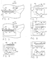
- Figure 4 shows the input wave guide 18 and a pair of rails 38, 40.
- the first end 58 of the first rail 38 is shown connected to the second end 64 of the second rail 40 by a conductive bridge 53 depicted as a fly lead.
- the first and second rails 38, 40 each have a respective first end 58, 60 and a second end 62, 64.
- the first end 58 of the first rail 55 is proximate or closest to the input face 22.
- the second end 64 of the second rail 40 is proximate or closest to the input face 22.
- the topology of Figure 4 shows an arrangement in which the conductive bridge 53 is connected between the first rail first end 58 and the second rail second end 64.
- the conductive network comprising the first and second rails 38, 40 and the conductive bridge 53 connecting the first and second rails are floating.
- a conductive path (not shown) from the conductive network to a reference potential such as a system voltage, signal source, or ground to prevent the network from developing a charge and assuming an undefined potential.
- Figures 1, 2 and 6 - 9 shows an embodiments in which the conductive bridge 53 is further characterized to include first and second bonding pads 55, 57 and a conductive jumper bridge 58 which is designed to be interrupted to permit an external drive circuit to drive the first and second rails to different potentials via external connections made to a first rail bonding pad 54 and to the second bonding pad 57.
- the conductive jumper bridge 58 can be interrupted by use of chemical means, a laser or mechanically with a scribe after which electrical contact with the rails could be made using a ball bonded or acoustically bonded lead between the first and second bonding pads 55, 57 or a soldered lead between the first and second bonding pads 55, 57.
- the circuit can also be restored via a small droplet of conductive epoxy or with a reflow of gold or equivalent material across the break in the conductive jumper bridge 58. If the first rail bonding pad 54 and the second rail bonding pad 55 were coupled to package pins, the conductive bridge 53 could be external to the package and operated to a conductive or open state under system control.
- Figure 5 shows the first rail conductive segment 54 connected from the first end of the first rail to the first bonding pad 55 and the second rail conductive segment connected from the second rail second end 64 to the second bonding pad 57.
- the conductive jumper bridge 58 connects the first bonding pad to the second bonding pad.
- Figure 6 shows an arrangement in which the first rail 38 first end 58 is connected to the first bonding pad 55.
- the second rail 40 second end 64 is connected to the second bonding pad 57.
- the first and second bonding pads 55, 57 are connected to each other via the conductive jumper bridge 58.
- Figure 7 shows an arrangement in which the first rail 38 first end 58 is connected to the first bonding pad 55.
- the second rail 40 first end 60 is connected to the second bonding pad 57.
- the first and second bonding pads 55, 57 are connected to each other via the conductive jumper bridge 58
- Figure 8. shows an embodiment in which the first rail 38 second end 62 is connected to the second bonding pad 57.
- the second rail 40 first end 60 is connected to the first bonding pad 55.
- the first and second bonding pads 55, 57 are connected to each other via the conductive jumper bridge 58.
- Figure 9 shows an embodiment in which the first rail 38 second end 62 is connected to the second bonding pad 57.
- the second rail second end 64 is connected to the second bonding pad 57.
- the first and second bonding pads 55, 57 are connected to each other via the conductive jumper bridge 58.
- the size of available dies might be a limitation on the use of such a means for interrupting and re-connecting the conductive jumper bridge.
- Alternative devices that might be investigated include the use of an optically coupled transistor or an E-PROM semiconductor switch.
- An n-channel J-FET might be preferable since it would require a negative drive voltage on its gate only during test when it might be desired to turn off the device.
- An N-Channel IGFET would require a positive gate voltage to turn it on to short the first and second conduction pads together, however, no drive power would be consumed.
- the process of manufacturing MIOC devices can be improved with the teaching of this patent to afford the maker with devices free of temperature driven hysteresis effects by adding the following steps to the method of forming an optic chip using conventional methods.
- the added steps will include the steps of:
- the invention relates to an Integrated Optics Chip comprising:
Landscapes
- Physics & Mathematics (AREA)
- Nonlinear Science (AREA)
- General Physics & Mathematics (AREA)
- Optics & Photonics (AREA)
- Chemical & Material Sciences (AREA)
- Engineering & Computer Science (AREA)
- Ceramic Engineering (AREA)
- Crystallography & Structural Chemistry (AREA)
- Optical Integrated Circuits (AREA)
- Optical Modulation, Optical Deflection, Nonlinear Optics, Optical Demodulation, Optical Logic Elements (AREA)
Applications Claiming Priority (2)
| Application Number | Priority Date | Filing Date | Title |
|---|---|---|---|
| US124457 | 1998-07-28 | ||
| US09/124,457 US6128424A (en) | 1998-03-31 | 1998-07-28 | Dual purpose input electrode structure for MIOCs (multi-function integrated optics chips) |
Publications (2)
| Publication Number | Publication Date |
|---|---|
| EP0977073A2 true EP0977073A2 (de) | 2000-02-02 |
| EP0977073A3 EP0977073A3 (de) | 2000-07-12 |
Family
ID=22415003
Family Applications (1)
| Application Number | Title | Priority Date | Filing Date |
|---|---|---|---|
| EP99114785A Withdrawn EP0977073A3 (de) | 1998-07-28 | 1999-07-28 | Doppelfunktion-Eingangselektrodentruktur für multifunktionale integrierte optische Chips ("MIOCs") |
Country Status (5)
| Country | Link |
|---|---|
| US (1) | US6128424A (de) |
| EP (1) | EP0977073A3 (de) |
| JP (2) | JP2000047160A (de) |
| CA (1) | CA2279068A1 (de) |
| IL (1) | IL131059A (de) |
Cited By (1)
| Publication number | Priority date | Publication date | Assignee | Title |
|---|---|---|---|---|
| CN104296735A (zh) * | 2013-11-29 | 2015-01-21 | 中国航空工业集团公司洛阳电光设备研究所 | 一种动力调谐陀螺仪信号器测量电路 |
Families Citing this family (10)
| Publication number | Priority date | Publication date | Assignee | Title |
|---|---|---|---|---|
| WO1999047955A1 (en) * | 1998-03-17 | 1999-09-23 | Minnesota Mining And Manufacturing Company | Passively compensated optical fibers |
| US20020110315A1 (en) * | 2001-02-15 | 2002-08-15 | Alcatel Usa Sourcing, L.P. | Pre-splitter module for conditioning optical signals in an access network |
| US6501867B2 (en) * | 2001-04-17 | 2002-12-31 | Lucent Technologies Inc. | Chirp compensated Mach-Zehnder electro-optic modulator |
| JP3929844B2 (ja) * | 2002-02-19 | 2007-06-13 | 株式会社フジクラ | 光スイッチ、光アドドロップモジュール及び光通信システム |
| US7426326B2 (en) * | 2004-03-12 | 2008-09-16 | The United States Of America As Represented By The Secretary Of The Navy | Low loss bridge electrode with rounded corners for electro-optic modulators |
| US7224869B2 (en) * | 2004-03-12 | 2007-05-29 | United States Of America As Represented By The Secretary Of The Navy | Low loss electrodes for electro-optic modulators |
| US9036954B2 (en) | 2011-04-01 | 2015-05-19 | Intel Corporation | Optical waveguide structure |
| US9231703B2 (en) * | 2011-11-14 | 2016-01-05 | Aci Communications, Inc. | Optical node configuration apparatus |
| JP6227069B1 (ja) | 2016-07-27 | 2017-11-08 | 富士通オプティカルコンポーネンツ株式会社 | 光変調器 |
| RU2764486C1 (ru) * | 2020-12-25 | 2022-01-17 | Публичное акционерное общество "Пермская научно-производственная компания" (ПАО "ПНППК") | Способ улучшения характеристик интегрально-оптической схемы (варианты) |
Family Cites Families (13)
| Publication number | Priority date | Publication date | Assignee | Title |
|---|---|---|---|---|
| JPS60257325A (ja) * | 1984-06-05 | 1985-12-19 | Yokogawa Hokushin Electric Corp | 光電圧センサ |
| GB8812180D0 (en) * | 1988-05-23 | 1988-06-29 | Bt & D Technologies Ltd | Electro-optic device |
| US5153930A (en) * | 1990-01-04 | 1992-10-06 | Smiths Industries Aerospace & Defense Systems, Inc. | Device employing a substrate of a material that exhibits the pyroelectric effect |
| JPH0734049B2 (ja) * | 1990-12-13 | 1995-04-12 | 日本航空電子工業株式会社 | 導波路型光デバイス |
| US5185823A (en) * | 1990-12-13 | 1993-02-09 | Japan Aviation Electronics Industry Limited | Waveguide type optical device |
| JP2758538B2 (ja) * | 1992-09-28 | 1998-05-28 | 松下電器産業株式会社 | 光変調素子と光変調装置及びその駆動方法 |
| JPH07120631A (ja) * | 1993-09-06 | 1995-05-12 | Ngk Insulators Ltd | 光導波路型部品 |
| JPH07113992A (ja) * | 1993-08-26 | 1995-05-02 | Ngk Insulators Ltd | 光導波路型部品 |
| US5388170A (en) * | 1993-11-22 | 1995-02-07 | At&T Corp. | Electrooptic device structure and method for reducing thermal effects in optical waveguide modulators |
| JP2894961B2 (ja) * | 1994-11-18 | 1999-05-24 | 日本電気株式会社 | 光制御デバイス |
| JP2746216B2 (ja) * | 1995-08-04 | 1998-05-06 | 日本電気株式会社 | 光スイッチ |
| JP2705664B2 (ja) * | 1995-09-18 | 1998-01-28 | 日本電気株式会社 | 光スイッチ |
| JP3742477B2 (ja) * | 1997-02-17 | 2006-02-01 | 富士通株式会社 | 光変調器 |
-
1998
- 1998-07-28 US US09/124,457 patent/US6128424A/en not_active Expired - Lifetime
-
1999
- 1999-07-23 IL IL13105999A patent/IL131059A/xx not_active IP Right Cessation
- 1999-07-28 CA CA002279068A patent/CA2279068A1/en not_active Abandoned
- 1999-07-28 EP EP99114785A patent/EP0977073A3/de not_active Withdrawn
- 1999-07-28 JP JP11213117A patent/JP2000047160A/ja not_active Withdrawn
-
2007
- 2007-10-01 JP JP2007257383A patent/JP4625491B2/ja not_active Expired - Lifetime
Cited By (1)
| Publication number | Priority date | Publication date | Assignee | Title |
|---|---|---|---|---|
| CN104296735A (zh) * | 2013-11-29 | 2015-01-21 | 中国航空工业集团公司洛阳电光设备研究所 | 一种动力调谐陀螺仪信号器测量电路 |
Also Published As
| Publication number | Publication date |
|---|---|
| US6128424A (en) | 2000-10-03 |
| IL131059A (en) | 2003-02-12 |
| EP0977073A3 (de) | 2000-07-12 |
| JP4625491B2 (ja) | 2011-02-02 |
| JP2000047160A (ja) | 2000-02-18 |
| JP2008026921A (ja) | 2008-02-07 |
| IL131059A0 (en) | 2001-01-28 |
| CA2279068A1 (en) | 2000-01-28 |
Similar Documents
| Publication | Publication Date | Title |
|---|---|---|
| JP4625491B2 (ja) | Mioc(多機能集積光素子)のための二用途入力電極 | |
| US5862276A (en) | Planar microphotonic circuits | |
| JP4928590B2 (ja) | ピロ電気効果による熱エラーを低減する集積光素子 | |
| US20110255147A1 (en) | Optical modulator | |
| US20050163412A1 (en) | Thin film electro-optical deflector device and a method of fabrication of such a device | |
| WO1988007220A1 (en) | Electro-optical switch | |
| US4904038A (en) | Guided wave optical frequency shifter | |
| US6438280B1 (en) | Integrated optics chip having reduced surface wave propagation | |
| US5621839A (en) | Optical waveguide device having substrate made of ferroelectric crystals | |
| US5999667A (en) | Method for reducing rejects in the manufacture of integrated optical components | |
| US5625726A (en) | Optical waveguide substrate, an article comprising the same and a substrate coupled thereto for holding optical fibers | |
| US5123065A (en) | Electro-optical transducer module | |
| JPH02504080A (ja) | 統合されたオプチック干渉計的ファイバジャイロスコープモジュール | |
| CN214375657U (zh) | 混合集成光电芯片以及光调制器、光纤陀螺 | |
| JPH07120631A (ja) | 光導波路型部品 | |
| EP0862075A1 (de) | Verfahren zur Verringerung von Ausschuss in der Herstellung von integrierten optischen Bauelementen | |
| EP0913666A2 (de) | Interferenzmessapparat und - Probe | |
| EP0211113A1 (de) | Optischer Wellenleiter Frequenzschieber | |
| JP2659786B2 (ja) | モード光分離器 | |
| JPH07113992A (ja) | 光導波路型部品 | |
| Ashley et al. | Components for IFOG based inertial measurement units using active and passive polymer materials | |
| CA1254642A (en) | Guided wave optical frequency shifter | |
| CN112859391A (zh) | 混合集成光电芯片以及光调制器、光纤陀螺 | |
| JPH07261044A (ja) | 光導波路デバイス及びその製造方法 | |
| JPH0361174B2 (de) |
Legal Events
| Date | Code | Title | Description |
|---|---|---|---|
| PUAI | Public reference made under article 153(3) epc to a published international application that has entered the european phase |
Free format text: ORIGINAL CODE: 0009012 |
|
| AK | Designated contracting states |
Kind code of ref document: A2 Designated state(s): DE FR GB IT |
|
| AX | Request for extension of the european patent |
Free format text: AL;LT;LV;MK;RO;SI |
|
| PUAL | Search report despatched |
Free format text: ORIGINAL CODE: 0009013 |
|
| AK | Designated contracting states |
Kind code of ref document: A3 Designated state(s): AT BE CH CY DE DK ES FI FR GB GR IE IT LI LU MC NL PT SE |
|
| AX | Request for extension of the european patent |
Free format text: AL;LT;LV;MK;RO;SI |
|
| 17P | Request for examination filed |
Effective date: 20010110 |
|
| AKX | Designation fees paid |
Free format text: DE FR GB IT |
|
| 17Q | First examination report despatched |
Effective date: 20060512 |
|
| GRAP | Despatch of communication of intention to grant a patent |
Free format text: ORIGINAL CODE: EPIDOSNIGR1 |
|
| STAA | Information on the status of an ep patent application or granted ep patent |
Free format text: STATUS: THE APPLICATION IS DEEMED TO BE WITHDRAWN |
|
| 18D | Application deemed to be withdrawn |
Effective date: 20080201 |