EP0976155B1 - Mehrlagige leiterplatte für hohe spannungen und hohe ströme sowie verfahren zur herstellung einer solchen - Google Patents
Mehrlagige leiterplatte für hohe spannungen und hohe ströme sowie verfahren zur herstellung einer solchen Download PDFInfo
- Publication number
- EP0976155B1 EP0976155B1 EP98907806A EP98907806A EP0976155B1 EP 0976155 B1 EP0976155 B1 EP 0976155B1 EP 98907806 A EP98907806 A EP 98907806A EP 98907806 A EP98907806 A EP 98907806A EP 0976155 B1 EP0976155 B1 EP 0976155B1
- Authority
- EP
- European Patent Office
- Prior art keywords
- circuit board
- printed circuit
- insulating
- plates
- metal plates
- Prior art date
- Legal status (The legal status is an assumption and is not a legal conclusion. Google has not performed a legal analysis and makes no representation as to the accuracy of the status listed.)
- Expired - Lifetime
Links
Images


Classifications
-
- H—ELECTRICITY
- H05—ELECTRIC TECHNIQUES NOT OTHERWISE PROVIDED FOR
- H05K—PRINTED CIRCUITS; CASINGS OR CONSTRUCTIONAL DETAILS OF ELECTRIC APPARATUS; MANUFACTURE OF ASSEMBLAGES OF ELECTRICAL COMPONENTS
- H05K1/00—Printed circuits
- H05K1/02—Details
- H05K1/0213—Electrical arrangements not otherwise provided for
- H05K1/0263—High current adaptations, e.g. printed high current conductors or using auxiliary non-printed means; Fine and coarse circuit patterns on one circuit board
- H05K1/0265—High current adaptations, e.g. printed high current conductors or using auxiliary non-printed means; Fine and coarse circuit patterns on one circuit board characterized by the lay-out of or details of the printed conductors, e.g. reinforced conductors, redundant conductors, conductors having different cross-sections
-
- H—ELECTRICITY
- H01—ELECTRIC ELEMENTS
- H01L—SEMICONDUCTOR DEVICES NOT COVERED BY CLASS H10
- H01L23/00—Details of semiconductor or other solid state devices
- H01L23/52—Arrangements for conducting electric current within the device in operation from one component to another, i.e. interconnections, e.g. wires, lead frames
- H01L23/538—Arrangements for conducting electric current within the device in operation from one component to another, i.e. interconnections, e.g. wires, lead frames the interconnection structure between a plurality of semiconductor chips being formed on, or in, insulating substrates
- H01L23/5383—Multilayer substrates
-
- H—ELECTRICITY
- H01—ELECTRIC ELEMENTS
- H01L—SEMICONDUCTOR DEVICES NOT COVERED BY CLASS H10
- H01L23/00—Details of semiconductor or other solid state devices
- H01L23/52—Arrangements for conducting electric current within the device in operation from one component to another, i.e. interconnections, e.g. wires, lead frames
- H01L23/538—Arrangements for conducting electric current within the device in operation from one component to another, i.e. interconnections, e.g. wires, lead frames the interconnection structure between a plurality of semiconductor chips being formed on, or in, insulating substrates
- H01L23/5386—Geometry or layout of the interconnection structure
-
- H—ELECTRICITY
- H01—ELECTRIC ELEMENTS
- H01L—SEMICONDUCTOR DEVICES NOT COVERED BY CLASS H10
- H01L25/00—Assemblies consisting of a plurality of individual semiconductor or other solid state devices ; Multistep manufacturing processes thereof
- H01L25/03—Assemblies consisting of a plurality of individual semiconductor or other solid state devices ; Multistep manufacturing processes thereof all the devices being of a type provided for in the same subgroup of groups H01L27/00 - H01L33/00, or in a single subclass of H10K, H10N, e.g. assemblies of rectifier diodes
- H01L25/04—Assemblies consisting of a plurality of individual semiconductor or other solid state devices ; Multistep manufacturing processes thereof all the devices being of a type provided for in the same subgroup of groups H01L27/00 - H01L33/00, or in a single subclass of H10K, H10N, e.g. assemblies of rectifier diodes the devices not having separate containers
- H01L25/07—Assemblies consisting of a plurality of individual semiconductor or other solid state devices ; Multistep manufacturing processes thereof all the devices being of a type provided for in the same subgroup of groups H01L27/00 - H01L33/00, or in a single subclass of H10K, H10N, e.g. assemblies of rectifier diodes the devices not having separate containers the devices being of a type provided for in group H01L29/00
- H01L25/072—Assemblies consisting of a plurality of individual semiconductor or other solid state devices ; Multistep manufacturing processes thereof all the devices being of a type provided for in the same subgroup of groups H01L27/00 - H01L33/00, or in a single subclass of H10K, H10N, e.g. assemblies of rectifier diodes the devices not having separate containers the devices being of a type provided for in group H01L29/00 the devices being arranged next to each other
-
- H—ELECTRICITY
- H01—ELECTRIC ELEMENTS
- H01L—SEMICONDUCTOR DEVICES NOT COVERED BY CLASS H10
- H01L2224/00—Indexing scheme for arrangements for connecting or disconnecting semiconductor or solid-state bodies and methods related thereto as covered by H01L24/00
- H01L2224/01—Means for bonding being attached to, or being formed on, the surface to be connected, e.g. chip-to-package, die-attach, "first-level" interconnects; Manufacturing methods related thereto
- H01L2224/42—Wire connectors; Manufacturing methods related thereto
- H01L2224/47—Structure, shape, material or disposition of the wire connectors after the connecting process
- H01L2224/48—Structure, shape, material or disposition of the wire connectors after the connecting process of an individual wire connector
- H01L2224/4805—Shape
- H01L2224/4809—Loop shape
- H01L2224/48091—Arched
-
- H—ELECTRICITY
- H01—ELECTRIC ELEMENTS
- H01L—SEMICONDUCTOR DEVICES NOT COVERED BY CLASS H10
- H01L2224/00—Indexing scheme for arrangements for connecting or disconnecting semiconductor or solid-state bodies and methods related thereto as covered by H01L24/00
- H01L2224/01—Means for bonding being attached to, or being formed on, the surface to be connected, e.g. chip-to-package, die-attach, "first-level" interconnects; Manufacturing methods related thereto
- H01L2224/42—Wire connectors; Manufacturing methods related thereto
- H01L2224/47—Structure, shape, material or disposition of the wire connectors after the connecting process
- H01L2224/48—Structure, shape, material or disposition of the wire connectors after the connecting process of an individual wire connector
- H01L2224/481—Disposition
- H01L2224/48151—Connecting between a semiconductor or solid-state body and an item not being a semiconductor or solid-state body, e.g. chip-to-substrate, chip-to-passive
- H01L2224/48221—Connecting between a semiconductor or solid-state body and an item not being a semiconductor or solid-state body, e.g. chip-to-substrate, chip-to-passive the body and the item being stacked
- H01L2224/48225—Connecting between a semiconductor or solid-state body and an item not being a semiconductor or solid-state body, e.g. chip-to-substrate, chip-to-passive the body and the item being stacked the item being non-metallic, e.g. insulating substrate with or without metallisation
- H01L2224/48227—Connecting between a semiconductor or solid-state body and an item not being a semiconductor or solid-state body, e.g. chip-to-substrate, chip-to-passive the body and the item being stacked the item being non-metallic, e.g. insulating substrate with or without metallisation connecting the wire to a bond pad of the item
-
- H—ELECTRICITY
- H01—ELECTRIC ELEMENTS
- H01L—SEMICONDUCTOR DEVICES NOT COVERED BY CLASS H10
- H01L2224/00—Indexing scheme for arrangements for connecting or disconnecting semiconductor or solid-state bodies and methods related thereto as covered by H01L24/00
- H01L2224/01—Means for bonding being attached to, or being formed on, the surface to be connected, e.g. chip-to-package, die-attach, "first-level" interconnects; Manufacturing methods related thereto
- H01L2224/42—Wire connectors; Manufacturing methods related thereto
- H01L2224/47—Structure, shape, material or disposition of the wire connectors after the connecting process
- H01L2224/48—Structure, shape, material or disposition of the wire connectors after the connecting process of an individual wire connector
- H01L2224/484—Connecting portions
- H01L2224/4847—Connecting portions the connecting portion on the bonding area of the semiconductor or solid-state body being a wedge bond
- H01L2224/48472—Connecting portions the connecting portion on the bonding area of the semiconductor or solid-state body being a wedge bond the other connecting portion not on the bonding area also being a wedge bond, i.e. wedge-to-wedge
-
- H—ELECTRICITY
- H01—ELECTRIC ELEMENTS
- H01L—SEMICONDUCTOR DEVICES NOT COVERED BY CLASS H10
- H01L2224/00—Indexing scheme for arrangements for connecting or disconnecting semiconductor or solid-state bodies and methods related thereto as covered by H01L24/00
- H01L2224/01—Means for bonding being attached to, or being formed on, the surface to be connected, e.g. chip-to-package, die-attach, "first-level" interconnects; Manufacturing methods related thereto
- H01L2224/42—Wire connectors; Manufacturing methods related thereto
- H01L2224/47—Structure, shape, material or disposition of the wire connectors after the connecting process
- H01L2224/49—Structure, shape, material or disposition of the wire connectors after the connecting process of a plurality of wire connectors
- H01L2224/491—Disposition
- H01L2224/49105—Connecting at different heights
- H01L2224/49109—Connecting at different heights outside the semiconductor or solid-state body
-
- H—ELECTRICITY
- H01—ELECTRIC ELEMENTS
- H01L—SEMICONDUCTOR DEVICES NOT COVERED BY CLASS H10
- H01L24/00—Arrangements for connecting or disconnecting semiconductor or solid-state bodies; Methods or apparatus related thereto
- H01L24/01—Means for bonding being attached to, or being formed on, the surface to be connected, e.g. chip-to-package, die-attach, "first-level" interconnects; Manufacturing methods related thereto
- H01L24/42—Wire connectors; Manufacturing methods related thereto
- H01L24/47—Structure, shape, material or disposition of the wire connectors after the connecting process
- H01L24/48—Structure, shape, material or disposition of the wire connectors after the connecting process of an individual wire connector
-
- H—ELECTRICITY
- H01—ELECTRIC ELEMENTS
- H01L—SEMICONDUCTOR DEVICES NOT COVERED BY CLASS H10
- H01L24/00—Arrangements for connecting or disconnecting semiconductor or solid-state bodies; Methods or apparatus related thereto
- H01L24/01—Means for bonding being attached to, or being formed on, the surface to be connected, e.g. chip-to-package, die-attach, "first-level" interconnects; Manufacturing methods related thereto
- H01L24/42—Wire connectors; Manufacturing methods related thereto
- H01L24/47—Structure, shape, material or disposition of the wire connectors after the connecting process
- H01L24/49—Structure, shape, material or disposition of the wire connectors after the connecting process of a plurality of wire connectors
-
- H—ELECTRICITY
- H01—ELECTRIC ELEMENTS
- H01L—SEMICONDUCTOR DEVICES NOT COVERED BY CLASS H10
- H01L2924/00—Indexing scheme for arrangements or methods for connecting or disconnecting semiconductor or solid-state bodies as covered by H01L24/00
- H01L2924/0001—Technical content checked by a classifier
- H01L2924/00014—Technical content checked by a classifier the subject-matter covered by the group, the symbol of which is combined with the symbol of this group, being disclosed without further technical details
-
- H—ELECTRICITY
- H01—ELECTRIC ELEMENTS
- H01L—SEMICONDUCTOR DEVICES NOT COVERED BY CLASS H10
- H01L2924/00—Indexing scheme for arrangements or methods for connecting or disconnecting semiconductor or solid-state bodies as covered by H01L24/00
- H01L2924/01—Chemical elements
- H01L2924/01039—Yttrium [Y]
-
- H—ELECTRICITY
- H01—ELECTRIC ELEMENTS
- H01L—SEMICONDUCTOR DEVICES NOT COVERED BY CLASS H10
- H01L2924/00—Indexing scheme for arrangements or methods for connecting or disconnecting semiconductor or solid-state bodies as covered by H01L24/00
- H01L2924/01—Chemical elements
- H01L2924/01057—Lanthanum [La]
-
- H—ELECTRICITY
- H01—ELECTRIC ELEMENTS
- H01L—SEMICONDUCTOR DEVICES NOT COVERED BY CLASS H10
- H01L2924/00—Indexing scheme for arrangements or methods for connecting or disconnecting semiconductor or solid-state bodies as covered by H01L24/00
- H01L2924/01—Chemical elements
- H01L2924/01068—Erbium [Er]
-
- H—ELECTRICITY
- H01—ELECTRIC ELEMENTS
- H01L—SEMICONDUCTOR DEVICES NOT COVERED BY CLASS H10
- H01L2924/00—Indexing scheme for arrangements or methods for connecting or disconnecting semiconductor or solid-state bodies as covered by H01L24/00
- H01L2924/01—Chemical elements
- H01L2924/01079—Gold [Au]
-
- H—ELECTRICITY
- H01—ELECTRIC ELEMENTS
- H01L—SEMICONDUCTOR DEVICES NOT COVERED BY CLASS H10
- H01L2924/00—Indexing scheme for arrangements or methods for connecting or disconnecting semiconductor or solid-state bodies as covered by H01L24/00
- H01L2924/15—Details of package parts other than the semiconductor or other solid state devices to be connected
- H01L2924/151—Die mounting substrate
- H01L2924/1515—Shape
- H01L2924/15153—Shape the die mounting substrate comprising a recess for hosting the device
-
- H—ELECTRICITY
- H01—ELECTRIC ELEMENTS
- H01L—SEMICONDUCTOR DEVICES NOT COVERED BY CLASS H10
- H01L2924/00—Indexing scheme for arrangements or methods for connecting or disconnecting semiconductor or solid-state bodies as covered by H01L24/00
- H01L2924/15—Details of package parts other than the semiconductor or other solid state devices to be connected
- H01L2924/151—Die mounting substrate
- H01L2924/1517—Multilayer substrate
-
- H—ELECTRICITY
- H01—ELECTRIC ELEMENTS
- H01L—SEMICONDUCTOR DEVICES NOT COVERED BY CLASS H10
- H01L2924/00—Indexing scheme for arrangements or methods for connecting or disconnecting semiconductor or solid-state bodies as covered by H01L24/00
- H01L2924/15—Details of package parts other than the semiconductor or other solid state devices to be connected
- H01L2924/181—Encapsulation
-
- H—ELECTRICITY
- H01—ELECTRIC ELEMENTS
- H01L—SEMICONDUCTOR DEVICES NOT COVERED BY CLASS H10
- H01L2924/00—Indexing scheme for arrangements or methods for connecting or disconnecting semiconductor or solid-state bodies as covered by H01L24/00
- H01L2924/30—Technical effects
- H01L2924/301—Electrical effects
- H01L2924/30107—Inductance
-
- H—ELECTRICITY
- H01—ELECTRIC ELEMENTS
- H01L—SEMICONDUCTOR DEVICES NOT COVERED BY CLASS H10
- H01L2924/00—Indexing scheme for arrangements or methods for connecting or disconnecting semiconductor or solid-state bodies as covered by H01L24/00
- H01L2924/30—Technical effects
- H01L2924/301—Electrical effects
- H01L2924/3025—Electromagnetic shielding
-
- H—ELECTRICITY
- H05—ELECTRIC TECHNIQUES NOT OTHERWISE PROVIDED FOR
- H05K—PRINTED CIRCUITS; CASINGS OR CONSTRUCTIONAL DETAILS OF ELECTRIC APPARATUS; MANUFACTURE OF ASSEMBLAGES OF ELECTRICAL COMPONENTS
- H05K2201/00—Indexing scheme relating to printed circuits covered by H05K1/00
- H05K2201/03—Conductive materials
- H05K2201/0332—Structure of the conductor
- H05K2201/0364—Conductor shape
- H05K2201/0376—Flush conductors, i.e. flush with the surface of the printed circuit
-
- H—ELECTRICITY
- H05—ELECTRIC TECHNIQUES NOT OTHERWISE PROVIDED FOR
- H05K—PRINTED CIRCUITS; CASINGS OR CONSTRUCTIONAL DETAILS OF ELECTRIC APPARATUS; MANUFACTURE OF ASSEMBLAGES OF ELECTRICAL COMPONENTS
- H05K3/00—Apparatus or processes for manufacturing printed circuits
- H05K3/0058—Laminating printed circuit boards onto other substrates, e.g. metallic substrates
- H05K3/0061—Laminating printed circuit boards onto other substrates, e.g. metallic substrates onto a metallic substrate, e.g. a heat sink
-
- H—ELECTRICITY
- H05—ELECTRIC TECHNIQUES NOT OTHERWISE PROVIDED FOR
- H05K—PRINTED CIRCUITS; CASINGS OR CONSTRUCTIONAL DETAILS OF ELECTRIC APPARATUS; MANUFACTURE OF ASSEMBLAGES OF ELECTRICAL COMPONENTS
- H05K3/00—Apparatus or processes for manufacturing printed circuits
- H05K3/10—Apparatus or processes for manufacturing printed circuits in which conductive material is applied to the insulating support in such a manner as to form the desired conductive pattern
- H05K3/107—Apparatus or processes for manufacturing printed circuits in which conductive material is applied to the insulating support in such a manner as to form the desired conductive pattern by filling grooves in the support with conductive material
-
- H—ELECTRICITY
- H05—ELECTRIC TECHNIQUES NOT OTHERWISE PROVIDED FOR
- H05K—PRINTED CIRCUITS; CASINGS OR CONSTRUCTIONAL DETAILS OF ELECTRIC APPARATUS; MANUFACTURE OF ASSEMBLAGES OF ELECTRICAL COMPONENTS
- H05K3/00—Apparatus or processes for manufacturing printed circuits
- H05K3/40—Forming printed elements for providing electric connections to or between printed circuits
- H05K3/42—Plated through-holes or plated via connections
- H05K3/429—Plated through-holes specially for multilayer circuits, e.g. having connections to inner circuit layers
-
- H—ELECTRICITY
- H05—ELECTRIC TECHNIQUES NOT OTHERWISE PROVIDED FOR
- H05K—PRINTED CIRCUITS; CASINGS OR CONSTRUCTIONAL DETAILS OF ELECTRIC APPARATUS; MANUFACTURE OF ASSEMBLAGES OF ELECTRICAL COMPONENTS
- H05K3/00—Apparatus or processes for manufacturing printed circuits
- H05K3/46—Manufacturing multilayer circuits
- H05K3/4611—Manufacturing multilayer circuits by laminating two or more circuit boards
- H05K3/4641—Manufacturing multilayer circuits by laminating two or more circuit boards having integrally laminated metal sheets or special power cores
Definitions
- the present invention relates to the field of PCB technology. It concerns a multilayer printed circuit board for high voltages and high currents, on which circuit board a plurality of individual circuit boards and first Insulating plates stacked one on top of the other and are firmly connected to each other, being within one individual circuit board as a conductor at least one metal plate is provided.
- Such a circuit board is for example from EP-A1-0 597 144 and is there for connecting one out hybrid power semiconductor arrangement consisting of several individual modules used.
- the invention further relates to a method of manufacture such a circuit board.
- the task is for a circuit board of the type mentioned kind solved in that the at least one metal plate each on its outer edge over the entire circumference of one second insulating plate is positively surrounded.
- Insulation weak points in the outer area of the metal plates avoid or reduce to a harmless minimum dimension.
- a second preferred embodiment of the circuit board according to The invention is characterized in that the at least a metal plate at least one bounded by an inner edge Has cutout, and that the inner edge of the at least a section of a third insulating plate form-fitting encloses.
- This can also make more complicated ones Geometries of the metal plate or the individual circuit board can be realized, for example - as in EP-A1-0 597 144 shown - openings for the reception of individual Enclose modules without causing a weakening the insulation comes in the area of the inner edges.
- a third preferred embodiment of the invention is thereby characterized in that the second and third insulating plates have the same thickness as the metal plates. hereby there is an edgeless, smooth transition between the metal plates and the insulating plates of each PCB.
- the single circuit board thus has a total on the top and bottom smooth surfaces that have a flat Gluing the circuit boards with the first insulating boards much easier in the stack and the risk of Drastically reduce defects between the plates.
- Another preferred embodiment of the invention is characterized in that the metal plates made of Cu and the first and second or third insulating plates made of a fiber-reinforced Insulating material, preferably a reinforced fabric Epoxy resin or a fabric-reinforced ceramic.
- a fiber reinforcement and in particular a fabric reinforcement preferably with a glass fabric
- the glass fabric protects the circuit board from delamination at extremely high currents (in the event of a short circuit: 500 kA!).
- a high structure is achieved with such a structure Stability and also a high resistance to environmental influences (Temperature, humidity, chemical resistance).
- the method according to the invention for producing a multilayer Printed circuit board is characterized in that in one first step by an outer edge with a predetermined Edge contour limited metal plates and those with a an inner edge with a corresponding edge contour limited cutout for the positive reception of the metal plates second insulating plates are provided that in a second step, the metal plates in each case provided section of the corresponding second insulating plate be fitted and together with the corresponding second insulating plate each form a single circuit board, and that in a third step the individuals thus formed Printed circuit boards together with first insulating boards in arranged in a stack and firmly connected.
- a preferred embodiment of the method according to the invention is characterized in that the metal plates with the second insulating plates before the third step of formation a uniform single circuit board on the edge are glued together and that the edge-side gluing done under vacuum. This will make the column between the metal plates and the second insulating plates are practical filled defect-free and the resulting individual circuit board forms a compact, stable unit, which is in the subsequent manufacturing step of stacking easily and can be handled safely.
- Fig. 10 is the section of the structure of EP-A1-0 597th 144 comparable hybrid module with a multi-layer circuit board according to a preferred embodiment of the invention shown.
- the multi-layer circuit board 36 serves as electrical connection for a plurality of individual semiconductor power modules 38, 39, appropriately and spaced from each other on a thermally well conductive plate-shaped heat sink 37 are arranged.
- the circuit board 36 consists of a multi-layer stack over the entire surface panels glued together, insulating panels 27, 30, Alternate 33 with individual circuit boards 25, 26. Each of the individual plates 25 to 27 and 30, 33 has in the range Semiconductor power modules 38, 39 corresponding cutouts, so that 36 recesses are formed in the circuit board which the modules can be used and accessed from above.
- the individual plates 25 to 27 and 30, 33 are in the example Fig. 10 shown with the same thickness D. It goes without saying by itself that depending on the requirements the insulation panels 27, 30, 33 and the individual circuit boards 25, 26 from each other can have different thicknesses. So for particularly high Currents the thickness of the individual circuit boards 25, 26 larger to get voted; but it can also handle particularly high voltages the thickness of the insulating plates 27, 30, 33 chosen larger become.
- the thickness D of the individual printed circuit boards is typically 1.5 mm.
- the individual circuit boards 25, 26 each contain one or more metal plate (s) 4 or 16, which the function the power line within the multilayer circuit board 36 take over.
- the metal plates 4, 16 preferably have the same thickness D as the individual printed circuit boards 25, 26.
- the special feature of the invention now consists in that the metal plates 4, 16 are not exposed between the Insulating plates 27, 30, 33 arranged and glued to them but that they are on their edges, both the Outside edges as well as possible inside edges, form-fitting enclosed by an insulating plate 1 or 13 of the same thickness are form-fitting (outer edges) or insulating plates 9 or 21 enclose (inner edges).
- Every single circuit board 25, 26 is thus made of one or more metal plates 4 or 16 and corresponding insulating plates 1, 9 and 13, 21, respectively, that interlock positively with close tolerance and are carefully glued together at the edges.
- the metal plates 4, 16 are in the stack of the multilayer PCB 36 fully embedded and against Harmful and stable environmental protection is protected.
- the embedding will in particular air gaps between the Avoided metal plates that are undesirable at high field strengths Partial discharges lead and operational safety the circuit board.
- the metal plates 4, 16 are preferably made of Cu and are - As already mentioned - typically 1.5 mm thick but also have other thicknesses.
- the insulating plates 1, 9 and 13, 21, as well as the insulating plates 27, 30, 33 are preferred made of a fiber-reinforced insulating material.
- the fiber reinforcement ensures in particular a dimensionally accurate Machinability and high mechanical stability, as well a coefficient of thermal expansion adapted to the metal plate (Cu).
- Insulating panels made of epoxy resin have proven particularly useful with glass fabric reinforcement or with a reinforcement non-woven aramid fibers, as they are commercially available under the name Duraver-E-Cu 104ML, Duraver-E-Cu 116ML or Duramid-P-Cu 115ML are available from Isola.
- Insulating panels made of glass fiber have proven themselves reinforced ceramics, e.g. under the label RO4003 / RO4350 are offered by Rogers.
- the gluing at the edges between the metal and insulating plate with suitable choice of the adhesive and the gap width a compensation of different thermal expansions between metal and insulating material.
- Proven as an adhesive have, for example, commercially available thermally curable Epoxy resin adhesive.
- connection between the semiconductor power modules 38, 39 and the metal plates 4, 16 (the conductor tracks) of the multilayer Printed circuit board 36 is, for example, via connection tabs 40 made that soldered to the modules at one end or are bonded, and at the other end they are in contact stand with the metal plates 4, 16.
- the plate stack is in addition, step-like in the area of the recesses for the modules constructed so that certain edge areas of the metal plates 4, 16 with the surface exposed and with the connecting straps 40 can be electrically connected.
- the production of the multilayer printed circuit board 36 according to FIG. 10 is preferably carried out in the context of the invention in FIG. 1 to 9 shown way.
- the individual circuit board 1 is first of all of a full-area (fabric-reinforced) insulating plate 1 (Fig. 1a), in which by a suitable machining process (milling, Cutting, sawing, laser cutting or the like) a cutout 2 is introduced, which is completely enclosed by the insulating plate 1 and is delimited by an inner edge 3 (Fig. 1b).
- the edge contour of the inner edge 3 corresponds as far as possible true to shape and exactly the edge contour of the outer edge of the metal plate (4 in Fig. 2), which is later inserted into the section 2 shall be.
- a suitable machining process milling, Cutting, sawing, laser cutting or the like
- a cutout 2 is introduced, which is completely enclosed by the insulating plate 1 and is delimited by an inner edge 3 (Fig. 1b).
- the edge contour of the inner edge 3 corresponds as far as possible
- a corresponding metal plate which preferably has the same thickness as the insulating plate 1, processed so that its outer edge 5 has a congruent edge contour with the edge contour 3 (Fig. 2a).
- Part of the metal plate 4 is, for example, a tab-like above connection area 6.
- the individual semiconductor power modules enclose.
- FIG. 3a to the metal plate 4 processed in this way (Fig. 3a) eight individual rectangular, frame-shaped insulating plates 9 produced, the outer edge 11 of the inner edge 8th the cutouts 7 in the metal plate 4 is adapted (Fig. 3b).
- the frame-shaped insulating plates 9 are made of the same Material and have the same thickness as the insulating plate 1. They each enclose a rectangular one an inner edge 12 limited cutout 10, in which later hybrid module, the individual semiconductor power modules are arranged. After the frame-shaped insulating plates 9 into the cutouts 7 provided in the metal plate 4 are fitted (Fig. 3c), the metal plate 4 is in turn in the cutout 2 provided in the insulating plate 1 fitted (Fig. 4).
- the two individual circuit boards 25 and 26 are finally (Fig. 9) together with further insulating plates 27, 30 and 33 alternately stacked one on top of the other to form a stack and glued together over the entire surface.
- the insulation panels too 27, 30 and 33 are preferably made of the same fabric reinforced Insulating material such as insulating plates 1, 9, 13 and 21. They also point in the appropriate places cutouts 28, 31, 34 delimited by inner edges 29, 32, 35 to accommodate the power modules.
- the ready glued Stack finally results in the multilayer printed circuit board 36, as shown in section in Fig. 10 and explained above has been.
- FIGS. 1 to 10 shows a particularly simple structure in which the multilayer Circuit board 36 only two individual circuit boards 25, 26, each with only one metal plate 4, 16 and without further has conductive connections.
- the multilayer Circuit board 36 only two individual circuit boards 25, 26, each with only one metal plate 4, 16 and without further has conductive connections.
- Within the scope of the invention can, however, also have a much more complicated circuit board can be realized in which not only more senior Layers, but also more complicated within the conductive layers Conductor structures and between the conductive layers electrical connections can be present.
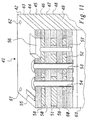
- a corresponding one The exemplary embodiment is excerpted in FIG. 11 played.
- the multilayer circuit board 41 has in this Fall a total of eight layers with three individual circuit boards 43, 45 and 47 and five insulating plates 42, 44, 46, 48 and 49.
- the individual circuit boards 43, 45 and 47 are relative complicated structures of metal plates 50, 51 and 52 housed that on the outer edge of appropriate insulating plates 58, 59 and 60 are surrounded.
- the individual layers of the multilayer printed circuit board 41 are different in this example thick.
- Recesses 56 can also be arranged here allow access to the underlying metal plate 50. It is also conceivable to pass through the stack Provide holes 57 through which, for example Wires or bolts are guided or pushed through can.
- isolated mounting holes 61, 62 are provided, by means of which the printed circuit board 41 together with an underlying cooling element 63 at the place of use can be attached.
Description
- hohe Festigkeit gegenüber thermischen Wechselbelastungen
- Teilentladungsfreiheit
- hohe Spannungsfestigkeit
- Beständigkeit gegenüber Umwelteinflüssen
- luftfreie Umschliessung der Leiterstrukturen
- hohe Delaminationsfestigkeit bei Kurzschlüssen
- gleicher thermischer Ausdehnungskoeffizient wie Leiterstrukturen
- hohe Kriechstromfestigkeit (hoher CTI-Wert)
- Material mit halogenfreiem Flammschutzmittel (UL VO)
- Fig. 1a,b
- ein erstes Exemplar einer für ein erstes bevorzugtes Ausführungsbeispiel der Erfindung vorgesehenen zweiten Isolierplatte vor (Fig. 1a) und nach (Fig. 1b) dem Einbringen des Ausschnitts, welcher für die formschlüssige Aufnahme einer Metallplatte vorgesehen ist;
- Fig. 2a,b
- eine für die Aufnahme in die Isolierplatte nach Fig. 1 vorgesehene Metallplatte mit angepasster Randkontur (Fig. 2a) und zusätzlich eingebrachten Ausschnitten (Fig. 2b);
- Fig. 3a-c
- ausgehend von der vorbereiteten Metallplatte nach Fig. 2b (Fig. 3a) die einzelnen Isolierplatten (Fig. 3b), welche zur Isolierung des Innenrandes in die Ausschnitte der Metallplatte formschlüssig eingesetzt werden (Fig. 3c);
- Fig. 4
- die mit den Isolierplatten nach Fig. 1b und Fig. 3b und der Metallplatte nach Fig. 2b gebildete einzelne Leiterplatte;
- Fig. 5a,b
- ein zweites Exemplar einer für erste bevorzugte Ausführungsbeispiel der Erfindung vorgesehenen zweiten Isolierplatte vor (Fig. 5a) und nach (Fig. 5b) dem Einbringen des Ausschnitts, welcher für die formschlüssige Aufnahme einer Metallplatte vorgesehen ist;
- Fig. 6a,b
- eine für die Aufnahme in die Isolierplatte nach Fig. 5 vorgesehene Metallplatte mit angepasster Randkontur (Fig. 6a) und zusätzlich eingebrachten Ausschnitten (Fig. 6b);
- Fig. 7a-c
- ausgehend von der vorbereiteten Metallplatte nach Fig. 6b (Fig. 7a) die einzelnen Isolierplatten (Fig. 7b), welche zur Isolierung des Innenrandes in die Ausschnitte der Metallplatte formschlüssig eingesetzt werden (Fig. 7c);
- Fig. 8
- die mit den Isolierplatten nach Fig. 5b und Fig. 7b und der Metallplatte nach Fig. 6b gebildete einzelne Leiterplatte;
- Fig. 9
- in der perspektivischen Explosionsdarstellung die den Stapel des Ausführungsbeispiels bildenden einzelnen Leiterplatten gemäss Fig. 4 und Fig. 8 und ersten Isolierplatten;
- Fig. 10
- im Schnitt den Aufbau eines zur EP-A1-0 597 144 vergleichbaren Hybridmoduls mit der mehrlagigen Leiterplatte gemäss Fig. 9, und
- Fig. 11
- in der perspektivischen Schnittansicht ein anderes Ausführungsbeispiel für eine Leiterplatte nach der Erfindung mit zusätzlichen Durchkontaktierungen, isolierten Befestigungsbohrungen und einem Kühlelement.
- es wird eine vollständige Isolation der Leiterbahnen nach aussen erreicht
- es wird eine hohe Teilentladungsaussetzspannung erreicht
- es wird eine hohe Zuverlässigkeit gegenüber Umwelteinflüssen (Temperatur, Luftfeuchtigkeit, Chemikalien) erreicht
- die geometrischen Abmasse sind genau einstellbar, so dass sich berechenbare konstante und induktionsarme elektrische Verbindungen ergeben
- es wird eine hohe Stabilität und Beständigkeit erreicht
- Gewebeverstärkungen in den Isolierplatten ergeben an die Cu-Leiter angepasste Ausdehnungskoeffizienten und verhindern Delaminationen
- ein zusätzliches Gehäuse kann bei Modulaufbauten unter Umständen entfallen
- viele Vorteile von Standard-Multilayer-Leiterplatten (Durchmetallisierungen, Einpresstechnik, Bestückung, Schriftdruck, Entwicklung mit Leiterplatten-CAD-Systemen) können übernommen werden
- es können zusätzliche Metallagen zur Verbesserung des EMC-Verhaltens (Abschirmung) vorgesehen werden.
- 1
- Isolierplatte
- 2
- Ausschnitt (Isolierplatte 1)
- 3
- Innenrand (Ausschnitt 2)
- 4
- Metallplatte (Cu)
- 5
- Aussenrand (Metallplatte 4)
- 6
- Anschlussbereich
- 7
- Ausschnitt (Metallplatte 4)
- 8
- Innenrand (Ausschnitt 7)
- 9
- Isolierplatte
- 10
- Ausschnitt (Isolierplatte 9)
- 11
- Aussenrand (Isolierplatte 9)
- 12
- Innenrand (Ausschnitt 10)
- 13
- Isolierplatte
- 14
- Ausschnitt (Isolierplatte 13)
- 15
- Innenrand (Ausschnitt 14)
- 16
- Metallplatte (Cu)
- 17
- Aussenrand (Metallplatte 16)
- 18
- Anschlussbereich
- 19
- Ausschnitt (Metallplatte 16)
- 20
- Innenrand (Ausschnitt 19)
- 21
- Isolierplatte
- 22
- Ausschnitt (Isolierplatte 21)
- 23
- Aussenrand (Isolierplatte 21)
- 24
- Innenrand (Ausschnitt 22)
- 25,26
- Leiterplatte
- 27,30,33
- Isolierplatte
- 28,31,34
- Ausschnitt
- 29, 32, 35
- Innenrand (Ausschnitt)
- 36,41
- mehrlagige Leiterplatte
- 37
- Kühlkörper
- 38,39
- Leistungsmodul (Halbleiter)
- 40
- Anschlusslasche
- 42,44,46
- Isolierplatte
- 43,45,47
- Leiterplatte
- 48,49
- Isolierplatte
- 50, 51, 52
- Metallplatte
- 53,54
- Durchkontaktierung
- 55
- Leiterbahn
- 56
- Ausnehmung
- 57
- Bohrung
- 58, 59, 60
- Isolierplatte
- 61,62
- Befestigungsbohrung (isoliert)
- 63
- Kühlelement
- D
- Dicke (Leiterplatte, Metallplatte)
Claims (12)
- Mehrlagige Leiterplatte (36, 41) für hohe Spannungen und hohe Ströme, bei welcher Leiterplatte (36, 41) eine Mehrzahl von einzelnen Leiterplatten (25, 26; 43, 45, 47) und ersten Isolierplatten (27, 30, 33; 42, 44, 46, 48, 49) in einem Stapel übereinander angeordnet und miteinander fest verbunden sind, wobei innerhalb einer einzelnen Leiterplatte (25, 26; 43, 45, 47) als Leiter jeweils wenigstens eine Metallplatte (4, 16; 50, 51, 52) vorgesehen ist, dadurch gekennzeichnet, dass die wenigstens eine Metallplatte (4, 16; 50, 51, 52) jeweils an ihrem Aussenrand (5, 17) über den gesamten Umfang von einer zweiten Isolierplatte (1 13; 58, 59, 60) formschlüssig umgeben ist.
- Leiterplatte nach Anspruch 1, dadurch gekennzeichnet, dass die wenigstens eine Metallplatte (4, 16) wenigstens einen von einem Innenrand (8 bzw. 20) begrenzten Ausschnitt (7 bzw. 19) aufweist, und dass der Innenrand (8 bzw. 20) des wenigstens einen Ausschnitts (7 bzw. 19) eine dritte Isolierplatte (9 bzw. 21) formschlüssig umschliesst.
- Leiterplatte nach einem der Ansprüche 1 und 2, dadurch gekennzeichnet, dass die zweiten bzw. dritten Isolierplatten (1, 13; 58, 59, 60 bzw. 9, 21) einstückig ausgebildet sind.
- Leiterplatte nach einem der Ansprüche 1 bis 3, dadurch gekennzeichnet, dass die zweiten bzw. dritten Isolierplatten (1, 13; 58, 59, 60 bzw. 9, 21) dieselbe Dicke (D2) aufweisen wie die Metallplatten (4, 16; 50, 51, 52).
- Leiterplatte nach einem der Ansprüche 1 bis 4, dadurch gekennzeichnet, dass die Metallplatten (4, 16; 50, 51, 52) aus Cu und die ersten und zweiten bzw. dritten Isolierplatten (27, 30, 33 bzw. 1, 13; 58, 59, 60 bzw. 9, 21) aus einem faserverstärkten Isoliermaterial, vorzugsweise einem gewebeverstärkten Epoxydharz oder einer gewebeverstärkten Keramik, bestehen.
- Leiterplatte nach einem der Ansprüche 1 bis 5, dadurch gekennzeichnet, dass die Metallplatten (4, 16; 50, 51, 52) an ihrem Aussenrand (5, 17) bzw. Innenrand (8, 20) mit den zweiten Isolierplatten (1, 13; 58, 59, 60) bzw. dritten Isolierplatten (9, 21) fest verbunden, insbesondere verklebt, sind.
- Leiterplatte nach einem der Ansprüche 1 bis 6, dadurch gekennzeichnet, dass zwischen den Metallplatten (50, 51, 52) unterschiedlicher Lagen der Leiterplatte (41) bzw. zwischen den Metallplatten (50, 51, 52) und den Oberflächen der Leiterplatte (41) Durchkontaktierungen (53, 54) vorgesehen sind.
- Verfahren zum Herstellen einer mehrlagigen Leiterplatte nach einem der Ansprüche 1 bis 7, dadurch gekennzeichnet, dass in einem ersten Schritt die durch einen Aussenrand (5, 17) mit vorgegebener Randkontur begrenzten Metallplatten (4, 16) und die mit einem durch einen Innenrand (3, 15) mit entsprechender Randkontur begrenzten Ausschnitt (2, 14) zur formschlüssigen Aufnahme der Metallplatten (4, 16) versehenen zweiten Isolierplatten (1, 13) bereitgestellt werden, dass in einem zweiten Schritt die Metallplatten (4 bzw. 16) jeweils in den dafür vorgesehenen Ausschnitt (2 bzw. 14) der entsprechenden zweiten Isolierplatte (1 bzw. 13) eingepasst werden und zusammen mit der entsprechenden zweiten Isolierplatte (1 bzw. 13) jeweils eine einzelne Leiterplatte (25 bzw. 26) bilden, und dass in einem dritten Schritt die so gebildeten einzelnen Leiterplatten (25, 26) zusammen mit ersten Isolierplatten (27, 30, 33) in einem Stapel angeordnet und miteinander fest verbunden werden.
- Verfahren nach Anspruch 8, dadurch gekennzeichnet, dass in dem ersten Schritt Metallplatten (4, 16) bereitgestellt werden, die zusätzlich wenigstens einen von einem Innenrand (8 bzw. 20) mit vorgegebener Randkontur begrenzten Ausschnitt (7 bzw. 19) aufweisen, dass in dem ersten Schritt weiterhin dritte Isolierplatten (9 bzw. 21) mit einem Aussenrand (11 bzw. 23) mit einer der Randkontur der Ausschnitte (7 bzw. 19) angepassten Randkontur bereitgestellt werden, und dass in dem zweiten Schritt die dritten Isolierplatten (9 bzw. 21) jeweils in den dafür vorgesehenen Ausschnitt (7 bzw. 19) der Metallplatten (4 bzw. 16) formschlüssig eingepasst werden.
- Verfahren nach einem der Ansprüche 8 und 9, dadurch gekennzeichnet, dass die Metallplatten (4, 16) mit den zweiten bzw. dritten Isolierplatten (1, 13 bzw. 9, 21) vor dem dritten Schritt zur Bildung einer einheitlichen einzelnen Leiterplatte (25 bzw. 26) randseitig miteinander verklebt werden.
- Verfahren nach Anspruch 10, dadurch gekennzeichnet, dass die randseitige Verklebung unter Vakuum erfolgt.
- Verfahren nach einem der Ansprüche 8 bis 11, dadurch gekennzeichnet, dass der Stapel aus den einzelnen Leiterplatten (25, 26) und ersten Isolierplatten (27, 30, 33) im dritten Schritt miteinander ganzflächig verklebt wird.
Applications Claiming Priority (3)
| Application Number | Priority Date | Filing Date | Title |
|---|---|---|---|
| CH00740/97A CH690806A5 (de) | 1997-03-27 | 1997-03-27 | Mehrlagiger Leiterplattenkörper für hohe Spannungen und hohe Ströme sowie Verfahren zur Herstellung eines solchen Leiterplattenkörpers. |
| CH74097 | 1997-03-27 | ||
| PCT/CH1998/000119 WO1998044557A1 (de) | 1997-03-27 | 1998-03-26 | Mehrlagige leiterplatte für hohe spannungen und hohe ströme sowie verfahren zur herstellung einer solchen |
Publications (2)
| Publication Number | Publication Date |
|---|---|
| EP0976155A1 EP0976155A1 (de) | 2000-02-02 |
| EP0976155B1 true EP0976155B1 (de) | 2002-09-04 |
Family
ID=4194109
Family Applications (1)
| Application Number | Title | Priority Date | Filing Date |
|---|---|---|---|
| EP98907806A Expired - Lifetime EP0976155B1 (de) | 1997-03-27 | 1998-03-26 | Mehrlagige leiterplatte für hohe spannungen und hohe ströme sowie verfahren zur herstellung einer solchen |
Country Status (7)
| Country | Link |
|---|---|
| EP (1) | EP0976155B1 (de) |
| JP (1) | JP2001516508A (de) |
| AT (1) | ATE223617T1 (de) |
| AU (1) | AU6606898A (de) |
| CH (1) | CH690806A5 (de) |
| DE (1) | DE59805420D1 (de) |
| WO (1) | WO1998044557A1 (de) |
Cited By (1)
| Publication number | Priority date | Publication date | Assignee | Title |
|---|---|---|---|---|
| RU2630680C2 (ru) * | 2015-09-21 | 2017-09-12 | Акционерное общество "Концерн "Моринформсистема - Агат" | Сильноточная многослойная печатная плата, содержащая слаботочные цепи управления |
Families Citing this family (2)
| Publication number | Priority date | Publication date | Assignee | Title |
|---|---|---|---|---|
| DE10051337A1 (de) * | 2000-10-17 | 2002-04-18 | Daimlerchrysler Rail Systems | Halbleitermodul mit Potentialabsteuerung |
| WO2017144599A1 (en) | 2016-02-24 | 2017-08-31 | Abb Schweiz Ag | Power module based on multi-layer circuit board |
Family Cites Families (6)
| Publication number | Priority date | Publication date | Assignee | Title |
|---|---|---|---|---|
| JPS57126154A (en) * | 1981-01-30 | 1982-08-05 | Nec Corp | Lsi package |
| DE3679627D1 (de) * | 1985-09-24 | 1991-07-11 | Contraves Ag | Mehrschichtige gedruckte schaltungsplatte. |
| US5223676A (en) * | 1989-11-27 | 1993-06-29 | The Furukawa Electric Co., Ltd. | Composite circuit board having means to suppress heat diffusion and manufacturing method of the same |
| WO1992017045A1 (en) * | 1991-03-25 | 1992-10-01 | Richard Hiram Womack | Multi-level/multi-layered hybrid package |
| US5285018A (en) * | 1992-10-02 | 1994-02-08 | International Business Machines Corporation | Power and signal distribution in electronic packaging |
| EP0597144A1 (de) * | 1992-11-12 | 1994-05-18 | IXYS Semiconductor GmbH | Hybride leistungselektronische Anordnung |
-
1997
- 1997-03-27 CH CH00740/97A patent/CH690806A5/de not_active IP Right Cessation
-
1998
- 1998-03-26 AT AT98907806T patent/ATE223617T1/de not_active IP Right Cessation
- 1998-03-26 JP JP54102598A patent/JP2001516508A/ja active Pending
- 1998-03-26 DE DE59805420T patent/DE59805420D1/de not_active Expired - Fee Related
- 1998-03-26 EP EP98907806A patent/EP0976155B1/de not_active Expired - Lifetime
- 1998-03-26 WO PCT/CH1998/000119 patent/WO1998044557A1/de active IP Right Grant
- 1998-03-26 AU AU66068/98A patent/AU6606898A/en not_active Abandoned
Cited By (1)
| Publication number | Priority date | Publication date | Assignee | Title |
|---|---|---|---|---|
| RU2630680C2 (ru) * | 2015-09-21 | 2017-09-12 | Акционерное общество "Концерн "Моринформсистема - Агат" | Сильноточная многослойная печатная плата, содержащая слаботочные цепи управления |
Also Published As
| Publication number | Publication date |
|---|---|
| JP2001516508A (ja) | 2001-09-25 |
| ATE223617T1 (de) | 2002-09-15 |
| DE59805420D1 (de) | 2002-10-10 |
| EP0976155A1 (de) | 2000-02-02 |
| CH690806A5 (de) | 2001-01-15 |
| AU6606898A (en) | 1998-10-22 |
| WO1998044557A1 (de) | 1998-10-08 |
Similar Documents
| Publication | Publication Date | Title |
|---|---|---|
| EP0976165B1 (de) | Piezoaktor mit neuer kontaktierung und herstellverfahren | |
| DE69633848T2 (de) | Leiterplattenfunkenstrecke | |
| EP0920055B1 (de) | Kühlvorrichtung für ein auf einer Leiterplatte angeordnetes, wärmeerzeugendes Bauelement | |
| EP0022176B1 (de) | Modul für Schaltungschips | |
| EP3231261B1 (de) | Leiterplatte mit einem asymmetrischen schichtenaufbau | |
| EP2724597B1 (de) | Elektronische baugruppe und verfahren zu deren herstellung | |
| WO2005089033A1 (de) | Steuergerät | |
| DE19928788A1 (de) | Elektronische Keramikkomponente | |
| EP3231262B1 (de) | Semiflexible leiterplatte mit eingebetteter komponente | |
| EP3815221A1 (de) | Aktiv gekühlte spule | |
| EP1060513B1 (de) | Halbleiterbauelement mit mehreren halbleiterchips | |
| DE3211538A1 (de) | Mehrschichten-stromschiene | |
| EP3095307B1 (de) | Leiterplatte, schaltung und verfahren zur herstellung einer schaltung | |
| EP1445799A2 (de) | Kühleinrichtung für Halbleiter auf Leiterplatte | |
| DE102011080153A1 (de) | Flexible verbindung von substraten in leistungshalbleitermodulen | |
| EP2649864A1 (de) | Leiterplatte | |
| DE4335946A1 (de) | Anordnung bestehend aus einer Leiterplatte | |
| EP0451541B1 (de) | Herstellung von mehrschichtigen Leiterplatten mit erhöhter Leiterbahnendichte | |
| EP0376100B1 (de) | Verfahren und Leiterplatte zum Montieren eines Halbleiter-Bauelements | |
| EP0976155B1 (de) | Mehrlagige leiterplatte für hohe spannungen und hohe ströme sowie verfahren zur herstellung einer solchen | |
| EP1480500B1 (de) | Leistungsversorgungsschaltung mit dreidimensional angeordneten Schaltungsträgern sowie Herstellungsverfahren | |
| DE102017109515A1 (de) | Halbleiteranordnung und Verfahren zu deren Herstellung | |
| DE102020133161A1 (de) | Drosselmodul und Verfahren zur Herstellung eines Drosselmoduls | |
| EP2964004A2 (de) | Elektronische bauteilanordnung | |
| DE19648492A1 (de) | Multi-Chip-Modul |
Legal Events
| Date | Code | Title | Description |
|---|---|---|---|
| PUAI | Public reference made under article 153(3) epc to a published international application that has entered the european phase |
Free format text: ORIGINAL CODE: 0009012 |
|
| 17P | Request for examination filed |
Effective date: 19990901 |
|
| AK | Designated contracting states |
Kind code of ref document: A1 Designated state(s): AT BE CH DE DK ES FI FR GB GR IE IT LI LU MC NL PT SE |
|
| GRAG | Despatch of communication of intention to grant |
Free format text: ORIGINAL CODE: EPIDOS AGRA |
|
| 17Q | First examination report despatched |
Effective date: 20010718 |
|
| GRAG | Despatch of communication of intention to grant |
Free format text: ORIGINAL CODE: EPIDOS AGRA |
|
| GRAH | Despatch of communication of intention to grant a patent |
Free format text: ORIGINAL CODE: EPIDOS IGRA |
|
| GRAH | Despatch of communication of intention to grant a patent |
Free format text: ORIGINAL CODE: EPIDOS IGRA |
|
| GRAA | (expected) grant |
Free format text: ORIGINAL CODE: 0009210 |
|
| AK | Designated contracting states |
Kind code of ref document: B1 Designated state(s): AT BE CH DE DK ES FI FR GB GR IE IT LI LU MC NL PT SE |
|
| PG25 | Lapsed in a contracting state [announced via postgrant information from national office to epo] |
Ref country code: NL Free format text: LAPSE BECAUSE OF FAILURE TO SUBMIT A TRANSLATION OF THE DESCRIPTION OR TO PAY THE FEE WITHIN THE PRESCRIBED TIME-LIMIT Effective date: 20020904 Ref country code: IT Free format text: LAPSE BECAUSE OF FAILURE TO SUBMIT A TRANSLATION OF THE DESCRIPTION OR TO PAY THE FEE WITHIN THE PRE;WARNING: LAPSES OF ITALIAN PATENTS WITH EFFECTIVE DATE BEFORE 2007 MAY HAVE OCCURRED AT ANY TIME BEFORE 2007. THE CORRECT EFFECTIVE DATE MAY BE DIFFERENT FROM THE ONE RECORDED.SCRIBED TIME-LIMIT Effective date: 20020904 Ref country code: IE Free format text: LAPSE BECAUSE OF FAILURE TO SUBMIT A TRANSLATION OF THE DESCRIPTION OR TO PAY THE FEE WITHIN THE PRESCRIBED TIME-LIMIT Effective date: 20020904 Ref country code: GR Free format text: LAPSE BECAUSE OF FAILURE TO SUBMIT A TRANSLATION OF THE DESCRIPTION OR TO PAY THE FEE WITHIN THE PRESCRIBED TIME-LIMIT Effective date: 20020904 Ref country code: GB Free format text: LAPSE BECAUSE OF FAILURE TO SUBMIT A TRANSLATION OF THE DESCRIPTION OR TO PAY THE FEE WITHIN THE PRESCRIBED TIME-LIMIT Effective date: 20020904 Ref country code: FR Free format text: LAPSE BECAUSE OF NON-PAYMENT OF DUE FEES Effective date: 20020904 Ref country code: FI Free format text: LAPSE BECAUSE OF FAILURE TO SUBMIT A TRANSLATION OF THE DESCRIPTION OR TO PAY THE FEE WITHIN THE PRESCRIBED TIME-LIMIT Effective date: 20020904 |
|
| REF | Corresponds to: |
Ref document number: 223617 Country of ref document: AT Date of ref document: 20020915 Kind code of ref document: T |
|
| REG | Reference to a national code |
Ref country code: GB Ref legal event code: FG4D Free format text: NOT ENGLISH |
|
| REG | Reference to a national code |
Ref country code: CH Ref legal event code: EP |
|
| REG | Reference to a national code |
Ref country code: CH Ref legal event code: NV Representative=s name: ISLER & PEDRAZZINI AG |
|
| REG | Reference to a national code |
Ref country code: IE Ref legal event code: FG4D Free format text: GERMAN |
|
| REF | Corresponds to: |
Ref document number: 59805420 Country of ref document: DE Date of ref document: 20021010 |
|
| PG25 | Lapsed in a contracting state [announced via postgrant information from national office to epo] |
Ref country code: SE Free format text: LAPSE BECAUSE OF FAILURE TO SUBMIT A TRANSLATION OF THE DESCRIPTION OR TO PAY THE FEE WITHIN THE PRESCRIBED TIME-LIMIT Effective date: 20021204 Ref country code: DK Free format text: LAPSE BECAUSE OF FAILURE TO SUBMIT A TRANSLATION OF THE DESCRIPTION OR TO PAY THE FEE WITHIN THE PRESCRIBED TIME-LIMIT Effective date: 20021204 |
|
| PG25 | Lapsed in a contracting state [announced via postgrant information from national office to epo] |
Ref country code: PT Free format text: LAPSE BECAUSE OF FAILURE TO SUBMIT A TRANSLATION OF THE DESCRIPTION OR TO PAY THE FEE WITHIN THE PRESCRIBED TIME-LIMIT Effective date: 20021213 |
|
| NLV1 | Nl: lapsed or annulled due to failure to fulfill the requirements of art. 29p and 29m of the patents act | ||
| GBV | Gb: ep patent (uk) treated as always having been void in accordance with gb section 77(7)/1977 [no translation filed] |
Effective date: 20020904 |
|
| PG25 | Lapsed in a contracting state [announced via postgrant information from national office to epo] |
Ref country code: LU Free format text: LAPSE BECAUSE OF NON-PAYMENT OF DUE FEES Effective date: 20030326 |
|
| PG25 | Lapsed in a contracting state [announced via postgrant information from national office to epo] |
Ref country code: ES Free format text: LAPSE BECAUSE OF FAILURE TO SUBMIT A TRANSLATION OF THE DESCRIPTION OR TO PAY THE FEE WITHIN THE PRESCRIBED TIME-LIMIT Effective date: 20030328 |
|
| PG25 | Lapsed in a contracting state [announced via postgrant information from national office to epo] |
Ref country code: MC Free format text: LAPSE BECAUSE OF NON-PAYMENT OF DUE FEES Effective date: 20030331 Ref country code: BE Free format text: LAPSE BECAUSE OF NON-PAYMENT OF DUE FEES Effective date: 20030331 |
|
| EN | Fr: translation not filed | ||
| PLBE | No opposition filed within time limit |
Free format text: ORIGINAL CODE: 0009261 |
|
| STAA | Information on the status of an ep patent application or granted ep patent |
Free format text: STATUS: NO OPPOSITION FILED WITHIN TIME LIMIT |
|
| REG | Reference to a national code |
Ref country code: IE Ref legal event code: FD4D Ref document number: 0976155E Country of ref document: IE |
|
| 26N | No opposition filed |
Effective date: 20030605 |
|
| BERE | Be: lapsed |
Owner name: *PPC ELECTRONIC A.G. Effective date: 20030331 |
|
| PGFP | Annual fee paid to national office [announced via postgrant information from national office to epo] |
Ref country code: CH Payment date: 20070117 Year of fee payment: 10 |
|
| PGFP | Annual fee paid to national office [announced via postgrant information from national office to epo] |
Ref country code: AT Payment date: 20070208 Year of fee payment: 10 |
|
| PGFP | Annual fee paid to national office [announced via postgrant information from national office to epo] |
Ref country code: DE Payment date: 20070226 Year of fee payment: 10 |
|
| REG | Reference to a national code |
Ref country code: CH Ref legal event code: PCAR Free format text: ISLER & PEDRAZZINI AG;POSTFACH 1772;8027 ZUERICH (CH) |
|
| REG | Reference to a national code |
Ref country code: CH Ref legal event code: PL |
|
| PG25 | Lapsed in a contracting state [announced via postgrant information from national office to epo] |
Ref country code: AT Free format text: LAPSE BECAUSE OF NON-PAYMENT OF DUE FEES Effective date: 20080326 |
|
| PG25 | Lapsed in a contracting state [announced via postgrant information from national office to epo] |
Ref country code: LI Free format text: LAPSE BECAUSE OF NON-PAYMENT OF DUE FEES Effective date: 20080331 Ref country code: DE Free format text: LAPSE BECAUSE OF NON-PAYMENT OF DUE FEES Effective date: 20081001 Ref country code: CH Free format text: LAPSE BECAUSE OF NON-PAYMENT OF DUE FEES Effective date: 20080331 |