EP0976055B1 - Datenwegarchitektur für schnellheit - Google Patents
Datenwegarchitektur für schnellheit Download PDFInfo
- Publication number
- EP0976055B1 EP0976055B1 EP96941436A EP96941436A EP0976055B1 EP 0976055 B1 EP0976055 B1 EP 0976055B1 EP 96941436 A EP96941436 A EP 96941436A EP 96941436 A EP96941436 A EP 96941436A EP 0976055 B1 EP0976055 B1 EP 0976055B1
- Authority
- EP
- European Patent Office
- Prior art keywords
- path
- cpu
- write
- read
- memory
- Prior art date
- Legal status (The legal status is an assumption and is not a legal conclusion. Google has not performed a legal analysis and makes no representation as to the accuracy of the status listed.)
- Expired - Lifetime
Links
Images

Classifications
-
- G—PHYSICS
- G06—COMPUTING; CALCULATING OR COUNTING
- G06F—ELECTRIC DIGITAL DATA PROCESSING
- G06F13/00—Interconnection of, or transfer of information or other signals between, memories, input/output devices or central processing units
- G06F13/38—Information transfer, e.g. on bus
- G06F13/40—Bus structure
- G06F13/4004—Coupling between buses
- G06F13/4022—Coupling between buses using switching circuits, e.g. switching matrix, connection or expansion network
Definitions
- This invention relates generally to microprocessor systems and more particularly, to microprocessor systems having first and second read paths and first and second write paths and buffers to isolate the first and second read paths and the first and second write paths.
- the semiconductor industry is increasingly characterized by a growing trend toward fabricating more circuits on a given semiconductor chip.
- the circuits are more complex in order to provide the higher performance required by end users of the semiconductor chips.
- To achieve the higher performance demanded by the end users it is necessary to not only provide more complexity in the circuits and functions, but also to ensure that the circuits are smaller and faster. This is being achieved not only by reducing the size of individual devices but by placing the circuits closer together. In turn, this means that more circuits have to be interconnected. The method of interconnection must not detract from the performance and speed of the various functions on the semiconductor chip.
- An interconnect provides a path or a medium for an electrical signal that is delivered from a source device to a destination or load device as illustrated in Figure 1, in which CPU 12 is a source device when writing to a load device such as PIC 24, SCU 26, or MCU 28, for example.
- the interconnect 40 connects CPU 40 to the load devices. As shown in Figure 1 there are usually more than one load device physically connected to the same interconnect.
- the capacitance relates to the amount of electrical charge that needs to be added to or taken out from the interconnect as the source voltage changes from a low to high or from a high to a low. The amount of charge depends upon the width and length of the interconnect as well as on the interconnects distance from other signal interconnects and power paths. Additionally, the input nodes of any load or distribution device also add to the capacitance load. These capacitance loads are generally higher than interconnect capacitance loads.
- This invention is a solution to this problem and is accomplished by physically isolating the bigger capacitance loads.
- the devices used for the isolation are multiplexors (muxes) and buffers.
- the muxes help to keep the capacitive loads of the driver ports separated and in this way signals from an active driver is not impeded by the capacitive loads for non-active drivers.
- the buffers isolate the capacitive loads of branches from the main trunk. As a result, the signals through the main trunk moves faster but still get transmitted to the branches. This ensures that regardless of how many branches there are, the signal transition times on the main trunk is not influenced the number of branches.
- EP-A-588 607 discloses a data processing apparatus having first and second read paths and first and second write paths.
- the respective first and second paths are each connectable by a switch.
- the active bus length can be reduced which, in turn, reduces the load capacity which thereby decreases wave form distortion and heightens the possible clock frequency.
- the present invention provides a microprocessor system having a CPU, a DMA unit, a memory, and at least one peripheral unit, wherein said microprocessor system comprises:
- FIG. 1 shows a prior art microprocessor system 10 having a CPU (central processing unit) 12, a DMA (direct memory access unit) 14, memory 16, and a bus interface unit 18 and steer logic 20 which comprises the basic microprocessor system.
- a number of peripheral units indicated at 22 are included in many microprocessor systems.
- Peripherals shown in Figure 1 are a PIC (Programmable Interrupt Controller) 24, an SCU (Serial Communications Unit) 26, an MCU (Memory Controller Unit) 28, a PCB (Peripheral Control Block) 30, a PMB (Power Management Unit) 32, a WDT (Watchdog Timer) 34, a TMR (Timer unit) 36, and a DMAC (Direct Memory Access Controller) 38.
- Bus 40 provides read and write capabilities between the CPU 12 and DMA 14, with peripherals 22 or memory 16.
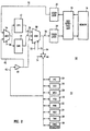
- Figure 2 shows an embodiment of the present invention. Elements in Figure 2 that are the same as elements in Figure 1 have the same numerical indicators as Figure 1.
- Figure 2 shows a microprocessor system 50 with a CPU 12, a DMA 14, a memory 16, a bus interface unit 18 and steer logic 20 and 20'.
- the steer logic 20 and 20' in Figure 2 is shown as two elements for discussion purposes, however, it should be understood that steer logic 20 and 20' can be a single element in microprocessor 50.
- the microprocessor system 50 also has a number of peripherals indicated at 22 that are shown as the same as those shown in Figure 1.
- isolation buffers isolate the basic read and write buses from the peripheral so that capacitances caused by the peripherals do not degrade the performance of the microprocessor system.
- Microprocessor system 50 in Figure 2 has a first read path 52 from memory 16 via bus interface unit 18 and steer logic unit 20 to CPU 12 and DMA 14 via a multiplexor 54.
- a first write path 56 connects CPU 12 and DMA 14 to memory 16 via multiplexor 58, steer logic 20', and bus interface unit 18.
- Multiplexor 58 is a three input multiplexor with an input from CPU 12, DMA 14 and an input from peripherals 22 via isolation buffer 60.
- the input from peripherals 22 via isolation buffer 60 provides internal peripheral read cycle data to an external data bus for program monitoring purposes. Program monitoring is used during the program development phase during which it helps to debug if internal peripheral read/write cycle data is observable at the outside pins of the semiconductor chip.
- a second read path 62 connects peripherals 22 to multiplexor 54 via isolation buffer 60.
- a second write path 64 connects CPU 12 and DMA 14 to peripherals 22 via isolation buffer 66.
- microprocessor system 50 The operation of microprocessor system 50 is as follows. First, for a memory read cycle, CPU 12 or DMA 14 initiates a data read cycle to fetch data from memory 16. A control unit (not shown) sends a select control signal to multiplexor 54 via select line 68 to select input from line 52. CPU 12 or DMA 14, whichever initiates the read cycle, uses the fetched data. During the write cycle, the control unit sends select control signals to multiplexor 58 via select lines 70 and 72. During this write cycle to memory, the control unit does not activate the control signal 74 to isolation buffer 66 which instructs isolation buffer 66 to not pass the data being sent on write path 56 to peripherals 22.
- control unit will instruct isolation buffer 66 to allow the data on write path 56 to be communicated to peripherals 22 via write path 64.
- peripherals 22 if monitoring is to be done, data from peripherals 22 is communicated to an external data bus (not shown) via isolation buffer 60 and multiplexor 58.
- the control unit sends select control information to multiplexor 58 via select control lines 70 and 72 and, at the same time, instructs isolation buffer 66 to not transmit data on write path 56 to peripherals 22.
- Isolation buffers 60 and 66 can be two logic gate inverters connected back-to-back. Because an inverter is a logic gate that delivers an output signal which is a logical inversion of the input the output of the two back-to-back inverters is in the same logic state as the input and hence there is no logic inversion in the signal as it passes through the buffer. The inverters also provide gains to the signal which influences its transition time. The main advantage of using a MOS buffer is because it isolates the input from the output and therefore the capacitance on the output interconnect does not load the input.
Landscapes
- Engineering & Computer Science (AREA)
- Physics & Mathematics (AREA)
- General Engineering & Computer Science (AREA)
- Theoretical Computer Science (AREA)
- Mathematical Physics (AREA)
- Computer Hardware Design (AREA)
- General Physics & Mathematics (AREA)
- Microcomputers (AREA)
- Bus Control (AREA)
Claims (3)
- Mikroprozessorsystem mit einer CPU, einer DMA-Einheit, einem Speicher und mindestens einer Peripherieeinheit, wobei das Mikroprozessorsystem aufweist:einen den Speicher mit der CPU und der DMA-Einheit verbindenden ersten Leseweg (52);einen die mindestens eine Peripherieeinheit und die CPU verbindenden zweiten Leseweg (62);einen den ersten Leseweg (52) vom zweiten Leseweg (62) trennenden ersten Puffer (60);einen im ersten und im zweiten Leseweg zwischen dem Speicher sowie der CPU und der DMA-Einheit angeordneten ersten Multiplexer, der den ersten Leseweg oder den zweiten Leseweg wählt;einen die CPU und den Speicher verbindenden ersten Schreibweg (56);einen die CPU und die DMA-Einheit mit der mindestens einen Peripherieeinheit verbindenden zweiten Schreibweg (64);einen den ersten Schreibweg vom zweiten Schreibweg trennenden zweiten Puffer (66), undeinen im ersten und im zweiten Schreibweg zwischen der CPU und der DMA-Einheit sowie dem Speicher angeordneten zweiten Multiplexer, der den ersten Schreibweg oder den zweiten Schreibweg wählt.
- Mikroprozessorsystem nach Anspruch 1, ferner mit einem die mindestens eine Peripherieeinheit über den ersten Schreibweg mit einem externen Datenbus verbindenden Überwachungsweg.
- Mikroprozessorsystem nach Anspruch 2, bei dem der zweite Multiplexer den ersten Schreibweg, den zweiten Schreibweg oder den Überwachungsweg wählt.
Applications Claiming Priority (3)
| Application Number | Priority Date | Filing Date | Title |
|---|---|---|---|
| US648523 | 1996-05-13 | ||
| US08/648,523 US5862408A (en) | 1996-05-13 | 1996-05-13 | Microprocessor system having multiplexor disposed in first and second read paths between memory CPU and DMA for selecting data from either read path |
| PCT/US1996/018717 WO1997043719A1 (en) | 1996-05-13 | 1996-11-22 | Data-path architecture for speed |
Publications (2)
| Publication Number | Publication Date |
|---|---|
| EP0976055A1 EP0976055A1 (de) | 2000-02-02 |
| EP0976055B1 true EP0976055B1 (de) | 2001-05-16 |
Family
ID=24601127
Family Applications (1)
| Application Number | Title | Priority Date | Filing Date |
|---|---|---|---|
| EP96941436A Expired - Lifetime EP0976055B1 (de) | 1996-05-13 | 1996-11-22 | Datenwegarchitektur für schnellheit |
Country Status (4)
| Country | Link |
|---|---|
| US (1) | US5862408A (de) |
| EP (1) | EP0976055B1 (de) |
| DE (1) | DE69612881T2 (de) |
| WO (1) | WO1997043719A1 (de) |
Families Citing this family (2)
| Publication number | Priority date | Publication date | Assignee | Title |
|---|---|---|---|---|
| US20050038946A1 (en) * | 2003-08-12 | 2005-02-17 | Tadpole Computer, Inc. | System and method using a high speed interface in a system having co-processors |
| US7660916B2 (en) * | 2005-06-16 | 2010-02-09 | Agere Systems Inc. | Emulation of independent active DMA channels with a single DMA capable bus master hardware and firmware |
Family Cites Families (13)
| Publication number | Priority date | Publication date | Assignee | Title |
|---|---|---|---|---|
| US4490785A (en) * | 1982-05-07 | 1984-12-25 | Digital Equipment Corporation | Dual path bus structure for computer interconnection |
| US4982321A (en) * | 1987-10-23 | 1991-01-01 | Honeywell Inc. | Dual bus system |
| US5289586A (en) * | 1988-11-29 | 1994-02-22 | Hitachi, Ltd. | Digital information transmission apparatus and method of driving information transmission bus system thereof |
| US5307468A (en) * | 1989-08-23 | 1994-04-26 | Digital Equipment Corporation | Data processing system and method for controlling the latter as well as a CPU board |
| US5185876A (en) * | 1990-03-14 | 1993-02-09 | Micro Technology, Inc. | Buffering system for dynamically providing data to multiple storage elements |
| US5333274A (en) * | 1991-10-15 | 1994-07-26 | International Business Machines Corp. | Error detection and recovery in a DMA controller |
| US5313627A (en) * | 1992-01-02 | 1994-05-17 | International Business Machines Corp. | Parity error detection and recovery |
| US5428746A (en) * | 1992-03-23 | 1995-06-27 | Zilog, Inc. | Integrated microprocessor unit generating separate memory and input-output device control signals |
| JP3226055B2 (ja) * | 1992-09-16 | 2001-11-05 | 松下電器産業株式会社 | 情報処理装置 |
| US5499384A (en) * | 1992-12-31 | 1996-03-12 | Seiko Epson Corporation | Input output control unit having dedicated paths for controlling the input and output of data between host processor and external device |
| US5426769A (en) * | 1993-08-26 | 1995-06-20 | Metalink Corp. | System and method for producing input/output expansion for single chip microcomputers |
| US5446845A (en) * | 1993-09-20 | 1995-08-29 | International Business Machines Corporation | Steering logic to directly connect devices having different data word widths |
| US5495573A (en) * | 1994-08-05 | 1996-02-27 | Unisys Corporation | Error logging system with clock rate translation |
-
1996
- 1996-05-13 US US08/648,523 patent/US5862408A/en not_active Expired - Lifetime
- 1996-11-22 WO PCT/US1996/018717 patent/WO1997043719A1/en active IP Right Grant
- 1996-11-22 EP EP96941436A patent/EP0976055B1/de not_active Expired - Lifetime
- 1996-11-22 DE DE69612881T patent/DE69612881T2/de not_active Expired - Lifetime
Also Published As
| Publication number | Publication date |
|---|---|
| EP0976055A1 (de) | 2000-02-02 |
| DE69612881D1 (de) | 2001-06-21 |
| WO1997043719A1 (en) | 1997-11-20 |
| US5862408A (en) | 1999-01-19 |
| DE69612881T2 (de) | 2002-03-28 |
Similar Documents
| Publication | Publication Date | Title |
|---|---|---|
| US5546563A (en) | Single chip replacement upgradeable computer motherboard with enablement of inserted upgrade CPU chip | |
| KR100288038B1 (ko) | 초대규모집적에 적합한 파이프라인 반도체장치 | |
| US5025412A (en) | Universal bus interface | |
| KR100309723B1 (ko) | 집적 회로 장치 | |
| US5101498A (en) | Pin selectable multi-mode processor | |
| US6980024B1 (en) | I/O circuitry shared between processor and programmable logic portions of an integrated circuit | |
| US5418911A (en) | Data path switch method and apparatus that provides capacitive load isolation | |
| US4057846A (en) | Bus steering structure for low cost pipelined processor system | |
| US20070247952A1 (en) | Semiconductor memory device and semiconductor integrated circuit device | |
| US5847450A (en) | Microcontroller having an n-bit data bus width with less than n I/O pins | |
| US6175886B1 (en) | Semiconductor integrated circuit with low-power bus structure and system for composing low-power bus structure | |
| EP1345126B1 (de) | Logikschaltung-implementierter Bustreiber | |
| JP2000039985A (ja) | レジスタファイル | |
| JP4015986B2 (ja) | 半導体集積回路装置 | |
| EP0976055B1 (de) | Datenwegarchitektur für schnellheit | |
| US6580288B1 (en) | Multi-property microprocessor with no additional logic overhead to shared pins | |
| US20040006664A1 (en) | System and method for efficient chip select expansion | |
| US5577215A (en) | Data transmission circuit for digital signal processor chip and method therefor | |
| JP3574061B2 (ja) | プロセッサ・バス構造 | |
| US6177808B1 (en) | Integration of bidirectional switches with programmable logic | |
| JPS62212860A (ja) | デ−タ転送回路 | |
| EP0929042B1 (de) | Bussteuerung in einem Datenprozessor | |
| JP2003085128A (ja) | 半導体装置 | |
| JPH04169982A (ja) | マイクロコンピュータ | |
| JPS58199490A (ja) | 半導体集積回路 |
Legal Events
| Date | Code | Title | Description |
|---|---|---|---|
| PUAI | Public reference made under article 153(3) epc to a published international application that has entered the european phase |
Free format text: ORIGINAL CODE: 0009012 |
|
| 17P | Request for examination filed |
Effective date: 19980921 |
|
| AK | Designated contracting states |
Kind code of ref document: A1 Designated state(s): DE ES GB |
|
| GRAG | Despatch of communication of intention to grant |
Free format text: ORIGINAL CODE: EPIDOS AGRA |
|
| 17Q | First examination report despatched |
Effective date: 20000809 |
|
| GRAG | Despatch of communication of intention to grant |
Free format text: ORIGINAL CODE: EPIDOS AGRA |
|
| GRAH | Despatch of communication of intention to grant a patent |
Free format text: ORIGINAL CODE: EPIDOS IGRA |
|
| GRAH | Despatch of communication of intention to grant a patent |
Free format text: ORIGINAL CODE: EPIDOS IGRA |
|
| GRAA | (expected) grant |
Free format text: ORIGINAL CODE: 0009210 |
|
| AK | Designated contracting states |
Kind code of ref document: B1 Designated state(s): DE ES GB |
|
| REF | Corresponds to: |
Ref document number: 69612881 Country of ref document: DE Date of ref document: 20010621 |
|
| PG25 | Lapsed in a contracting state [announced via postgrant information from national office to epo] |
Ref country code: ES Free format text: LAPSE BECAUSE OF FAILURE TO SUBMIT A TRANSLATION OF THE DESCRIPTION OR TO PAY THE FEE WITHIN THE PRESCRIBED TIME-LIMIT Effective date: 20011130 |
|
| REG | Reference to a national code |
Ref country code: GB Ref legal event code: IF02 |
|
| PLBE | No opposition filed within time limit |
Free format text: ORIGINAL CODE: 0009261 |
|
| STAA | Information on the status of an ep patent application or granted ep patent |
Free format text: STATUS: NO OPPOSITION FILED WITHIN TIME LIMIT |
|
| 26N | No opposition filed | ||
| PGFP | Annual fee paid to national office [announced via postgrant information from national office to epo] |
Ref country code: DE Payment date: 20151118 Year of fee payment: 20 Ref country code: GB Payment date: 20151118 Year of fee payment: 20 |
|
| REG | Reference to a national code |
Ref country code: DE Ref legal event code: R071 Ref document number: 69612881 Country of ref document: DE |
|
| REG | Reference to a national code |
Ref country code: GB Ref legal event code: PE20 Expiry date: 20161121 |
|
| PG25 | Lapsed in a contracting state [announced via postgrant information from national office to epo] |
Ref country code: GB Free format text: LAPSE BECAUSE OF EXPIRATION OF PROTECTION Effective date: 20161121 |