EP0970503B1 - Gasgefülter rückstrevelektronendetektor für rasterelektronenmikroskop unterkontrollierter umgebung - Google Patents
Gasgefülter rückstrevelektronendetektor für rasterelektronenmikroskop unterkontrollierter umgebung Download PDFInfo
- Publication number
- EP0970503B1 EP0970503B1 EP99900089A EP99900089A EP0970503B1 EP 0970503 B1 EP0970503 B1 EP 0970503B1 EP 99900089 A EP99900089 A EP 99900089A EP 99900089 A EP99900089 A EP 99900089A EP 0970503 B1 EP0970503 B1 EP 0970503B1
- Authority
- EP
- European Patent Office
- Prior art keywords
- electron
- backscattered
- specimen
- signals
- detector
- Prior art date
- Legal status (The legal status is an assumption and is not a legal conclusion. Google has not performed a legal analysis and makes no representation as to the accuracy of the status listed.)
- Expired - Lifetime
Links
Images
Classifications
-
- H—ELECTRICITY
- H01—ELECTRIC ELEMENTS
- H01J—ELECTRIC DISCHARGE TUBES OR DISCHARGE LAMPS
- H01J37/00—Discharge tubes with provision for introducing objects or material to be exposed to the discharge, e.g. for the purpose of examination or processing thereof
- H01J37/02—Details
- H01J37/244—Detectors; Associated components or circuits therefor
-
- H—ELECTRICITY
- H01—ELECTRIC ELEMENTS
- H01J—ELECTRIC DISCHARGE TUBES OR DISCHARGE LAMPS
- H01J2237/00—Discharge tubes exposing object to beam, e.g. for analysis treatment, etching, imaging
- H01J2237/26—Electron or ion microscopes
- H01J2237/2602—Details
- H01J2237/2605—Details operating at elevated pressures, e.g. atmosphere
- H01J2237/2608—Details operating at elevated pressures, e.g. atmosphere with environmental specimen chamber
Definitions
- This invention relates to the field of environmental scanning electron microscopes ("ESEM”), and more particularly to a gaseous backscattered electron detector for an environmental scanning electron microscope which is intended to collect only a backscattered electron signal in the gaseous environment of the ESEM.
- ESEM environmental scanning electron microscopes
- the advantages of an environmental scanning electron microscope over the standard scanning electron microscope (“SEM”) lie in its ability to produce high-resolution electron images of moist or non-conductive specimens (e.g., biological materials, plastics, ceramics, fibers) which are extremely difficult to image in the usual vacuum environment of the SEM.
- the environmental scanning electron microscope allows the specimen to be maintained in its "natural” state, without subjecting it to the distortions caused by drying, freezing, or vacuum coating normally required for high-vacuum electron beam observation.
- the relatively high gas pressure easily tolerated in the ESEM specimen chamber acts effectively to dissipate the surface charge that would normally build up on a non-conductive specimen, blocking high quality image acquisition.
- the environmental scanning electron microscope also permits direct, real-time observation of liquid transport, chemical reaction, solution, hydration, crystallization, and other processes occurring at relatively high vapor pressures, far above those that can be permitted in the normal SEM specimen chamber.
- the electron beam is emitted by an electron gun and passes through an electron optical column with an objective lens assembly having a final pressure limiting aperture at its lower end thereof.
- the electron beam passes through magnetic lenses which are used to focus the beam and direct the electron beam through the final pressure limiting aperture.
- the beam is subsequently directed into a specimen chamber through the final pressure limiting aperture wherein it impinges upon a specimen supported upon the specimen stage.
- the specimen stage is positioned for supporting the specimen approximately 1 to 25 mm below the final pressure limiting aperture so as to allow the beam of electrons to interact with the specimen.
- the specimen chamber is disposed below the optical vacuum column and is capable of maintaining the sample enveloped in gas, typically water vapor, at a pressure of approximately between 1,3 N/m 2 and 6,6 kN/m 2 (10 -2 and 50 Torr) in registration with the final pressure limiting aperture such that a surface of the specimen may be exposed to the charged particle beam emitted from the electron gun and directed through the final pressure limiting aperture.
- U.S. Pat. No. 4,880,976 describes the design and need for a gaseous secondary electron detector for an ESEM. Subsequent prior art describe improved secondary electron detectors and detectors that detect backscattered electrons, such as in U.S. Pat. No. 4,897,545.
- the conventional high vacuum SEM has an SE detector as standard and most users also purchase a separate BSE detector.
- a fundamental aspect of an ESEM detector is the amplification of the electron signal in the gaseous environment of the specimen chamber. This is important because the electron signal levels used in an SEM are normally too small to be directly connected to an amplifier. The noise from the amplifier would be too high to make the SEM a practical instrument.
- the secondary electron signal is amplified (with negligible added noise) by a photomultiplier as part of a complex arrangement originally described by Everhart and Thomley.
- this type of detector is commonly called the Everhart-Thomley (E-T) detector.
- the E-T detector will not function in the ESEM because the high voltages used will discharge in the gas environment of the ESEM.
- an environmental scanning electron microscope provides a device for generating, amplifying and detecting secondary and backscattered electrons emanating from a surface of a sample being examined.
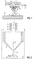
- a beam of electrons 10 is emitted through an electron optical column of an objective lens assembly 11 by an electron gun (not shown).
- the vacuum optical column includes a final limiting pressure aperture 14 at its lower end thereof.
- a beam 10 is directed into a specimen chamber 16 wherein it impinges upon a specimen 18 supported on a specimen stage 20.
- the specimen mount or stage 20 is located within the specimen chamber 16 and is positioned for supporting specimen 18 approximately 1 to 25mm, and preferably 1 to 10mm, below final pressure limiting aperture 14 so as to allow the beam of electrons to interact with the specimen.
- the specimen chamber is disposed below the optical vacuum column and is capable of maintaining the sample 18 enveloped in gas, preferably nitrogen or water vapor, at a pressure of approximately between 1,3 N/m 2 and 6,6 kN/m 2 (10 -2 and 50 Torr) in registration with the pressure limiting aperture such that a surface of the specimen may be exposed to the charged particle beam emitted from the electron gun and emitted through the pressure limiting aperture 14.
- the ESEM detectors use an electric field in the gas to amplify an electron signal.
- the electron field between the sample 18 and the detector electrode 22, held at a positive voltage accelerates a signal electron, as at 24 until it has enough energy to ionize a gas molecule which also liberates another electron, as represented by reference numeral 27 in Fig. 1.
- the two electrons will be further accelerated to thereby generate more electrons, as at 28.
- This process can generate enough amplification for the electron current to be passed directly to a low noise amplifier 30.
- the amplification is typically in the range of 100 to 2,000.
- the amplification principle applies to any electron that is in the gas.
- Figure 1 illustrates amplification of the low energy "secondary electrons" generated at the surface of the specimen.
- Electrons can also be generated in the gas by backscattered electrons ("BSE"). These are high-energy electrons from the primary beam that are reflected from the sample.
- BSEs have a high velocity and this high velocity reduces the chance that the BSE will strike a molecule in the gas between the sample and the detector. Hence, it has been found that only a small fraction of the BSE will generate a useful gas interaction. Accordingly, most of the signals collected by the detector electrode are generated by amplification of the secondary electrons.
- U.S. Pat. No. 5,362,964 describes improvements in the design of a gaseous detector for an ESEM to maximize the SE collection while minimizing the collection of signals generated by other sources such as BSE. It has therefore been found desirable to provide a detector configuration for an ESEM that is designed to collect only signals generated by the BSE.
- U.S. Pat. 4,897,545 to Danilatos describes a multi-electrode structure wherein the different electrodes will collect different proportions of SE and BSE information. Some electrodes collect a signal that is rich in SE, and some collect a signal that is rich in BSE.
- the '545 patent does not relate to an electrode detector that collects only the BSE signal.
- prior art exists which converts backscattered electrons (BSE) into secondary electrons (SE) and then collects the resulting SE signal -- but only in high-vacuum SEMs.
- BSE backscattered electrons
- SE secondary electrons
- a dedicated gaseous electron detector for an environmental scanning electron microscope that is intended to collect only backscattered electron signals.
- an electron detector is employed and electron beam is generated by an electron gun which passes through an electron optical column until the electron beam is focused and scanned across the diameter of the final pressure limiting aperture provided at the lower end of the electron optical column.
- the final pressure limiting aperture separates the relatively high vacuum of the electron optical column from the relatively low vacuum of the specimen chamber.
- the specimen chamber is positioned below the electron optical column and is capable of maintaining the specimen enveloped in gas in registration with the final pressure limiting aperture such that a surface of the specimen may be exposed to the focused beam of electrons.
- a specimen stage is located within the specimen chamber and is positioned for supporting the specimen approximately 1 to 10 mm below the final pressure limiting aperture so as to allow the focused beam of electrons to interact with the specimen.
- the specimen is maintained at a pressure between about 1,3 N/m 2 and 6,6 kN/m 2 (10 -2 and 50 Torr), and preferable approximately 0,13 to 1,3 kN/m 2 (1 to 10 Torr).
- the present invention includes a detector assembly including a negatively biased converter plate upon which backscattered electrons emanating from the surface of the sample impinge to thereby generate secondary electrons at the surface thereof. These secondary electrons are referred to as "converted backscattered electrons.”
- the converter plate also serves as the final pressure limiting aperture between the specimen chamber and the electron column.
- the detector assembly further includes a detector member which collects only the converted backscattered electrons generated by the converter plate.
- this detector member can be in the form of a collection grid, a collection plate or a collector ring.
- the electron beam passes through a central opening in the converter plate and then through an aperture in the detector member before striking the specimen in the specimen chamber.
- the detector member is held at zero potential and accordingly does not collect the secondary electron signal generated at the specimen.
- the backscattered electrons will pass through an aperture arrangement in the detector member and strike the converter plate.
- secondary electrons are generated at the surface of the converter plate (the "converted backscattered electrons").
- the converted backscattered electrons are then amplified in the gas of the specimen chamber by the electric field created between the converter plate and the detector member, in the same way that the secondary electrons are amplified in the conventional gaseous secondary electron detectors.
- the spacing between the converter plate and the collector grid/plate/ring is preferably in the range of approximately 1 to 5mm. Therefore, the detector member configuration (i.e., the collection grid, the collection plate or the collector ring) does not collect a secondary electron signal from the sample but only collects an amplified converted backscattered electron signal.
- the efficiency of the converter plate may be increased by making the converter plate from a material that converts the backscattered electrons to secondary electrons efficiently. Therefore, in the preferred embodiments, the converter plate is preferably made from gold or coated with magnesium or other materials known to generate a high yield of secondary electrons from the backscattered electrons.
- the present invention also relates to an environmental scanning electron microscope comprising means for generating and directing an electron beam from an electron column towards a specimen enveloped in a gaseous environment of a specimen chamber, and dual detector means for detecting both secondary electron signals and backscattered electron signals emanating from the specimen and being capable of switching between the detection of secondary electron signals and backscattered electron signals with said detector means being positioned in the gaseous environment of the specimen.
- said dual detector means includes a converter plate biased at a voltage V2 upon which backscattered electrons emanating from the surface of the specimen impinge upon to thereby create converted backscattered electrons and further includes means for collecting secondary and backscattered electron signals biased at a voltage V1 which is positioned below said converter plate in said specimen chamber and wherein Vg is the voltage to obtain the required amplification of the electron signals in the gaseous environment of the specimen chamber so that secondary electron signals are only detected by said dual detector means if V1 is equal to +Vg and V2 is equal to +Vg, backscattered electron signals are only detected if V1 is 0 V and V2 is -Vg, and both secondary and backscattered electron signals are detected if V1 is +Vg and V2 is between -Vg and +Vg.
- Vg is the voltage to obtain the required amplification of the electron signal
- secondary electron signals are only detected by the dual detector if the converter plate is biased at the voltage of +Vg and the detector member is biased at a voltage of +Vg.
- backscattered electron signals are only detected if the converter plate is biased at a voltage of -Vg and the detector member is biased at OV.
- both secondary and backscattered electron signals can be detected if the voltage applied to the detector member is +Vg and the voltage applied to the converter plate is between -Vg and +Vg. Accordingly, a dual electron detector arrangement has been designed that can be easily switched between secondary electron detection, backscattered electron detection or both together.
- an insulating cone is sealed underneath the converter plate.
- the aperture of the insulating cone forms the pressure limiting aperture which is thereby much closer to the sample.
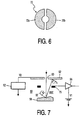
- the detector member is formed to be symmetrical about the electron beam axis. Therefore, the detector member is in the form of a split collecting device. The signals from the two segments of the split collecting device are added to give the normal material contrast and subtracted to obtain a topographic image.
- FIG. 2 the prior environmental scanning electron microscope of U.S. Patent Nos. 5,362,964 and 5,412,211 is illustrated.
- a device for generating, amplifying and detecting secondary and backscattered electrons emanating from a surface of a sample being examined is provided. More specifically, a beam of electrons 32 is emitted through an electron optical column 34 and the objective lens assembly 31 by an electron gun (not shown). Within the electron optical column 34, the electron beam is subjected to a differential pumping system as is disclosed in U.S. Patent Nos. 4,823,006 and 5,250,808.
- the electron optical column 34 includes a final pressure limiting aperture 36 at its lower end.
- the beam is subsequentially directed into a specimen chamber 42 through final pressure limiting aperture 36 wherein it impinges upon a specimen 44 supported on a specimen stage 46.
- the specimen mount or stage 46 is located within the specimen chamber 42 and is positioned for supporting specimen 44 approximately 1 to 25 mm, and preferably 1 to 10 mm, below final pressure limiting aperture 36 so as to allow the beam of electrons to interact with the specimen.
- the specimen chamber 42 is disposed below the electron optical column 34 and is capable of maintaining the sample 44 enveloped in gas, preferably nitrogen or water vapor, at a pressure of approximately between 1,3 N/m 2 and 6,6 kN/m 2 (10 -2 to 50 Torr) in registration with the final pressure limiting aperture 36 such that a surface of the specimen may be exposed to the charged particle beam emitted from the electron gun and directed through the final pressure limiting aperture 36.
- gas preferably nitrogen or water vapor
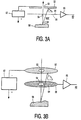
- FIG. 3A A preferred embodiment of a dedicated gaseous backscattered electron detector which collects only backscattered electron signals is illustrated in Figure 3A.
- the electron beam from the electron optical column passes through a central opening 50 in a convertor plate 52 and then through a central aperture 54 of a detector member 56 before the sample 58.
- the converter plate 52 also serves as the pressure limiting aperture between the specimen chamber and the electron column (corresponding with 36 in Fig. 2).
- the detector member 56 is in the form of a collection grid having a wire mesh structure.
- the converter plate 52 and the collection grid 56 are supported in the gaseous environment of the ESEM specimen chamber 60.
- the collection grid 56 is held at ground potential and accordingly does not collect the secondary electron signal generated at the specimen.
- the converter plate 52 is held at a negative voltage by a power supply 62.
- the backscattered electrons (or BSE) 63 will pass through perforations 64 provided in the wire mesh structure of the collection grid 56 and strike the converter plate 52. This will generate secondary electrons at the surface of the converter plate 52. For sake of simplification, these secondary electrons generated at the surface of the converter plate 52 are referred to herein as "converted backscattered electrons". These converted backscattered electrons are amplified in the gas of the specimen chamber by the electric field created between the converter plate 52 and the collection grid 56 in the same way that secondary electrons emanating from the surface of the sample are amplified in the conventional gaseous secondary electron detectors.
- an electron detector configuration is designed that does not collect any secondary electron signals but instead collects only an amplified converted BSE signal.
- the collection grid 56 is replaced by a collection plate 66.
- the collection plate 66 has a relatively large central aperture 68 to allow the BSE to pass therethrough, but is small enough that the converted BSE are adequately collected.
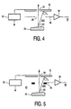
- FIG. 5 illustrates an alternative dedicated gaseous electron detector wherein a collector ring 70 is utilized to collect the amplified converted BSE signals.
- the collector ring 70 is preferably circular and the area thereof is small enough to allow most of the backscattered electron to pass unobstructed to the converter plate 52.
- the signal electrodes may become dirty with material generated by sample experimentation. It is therefore desirable that the signal electrodes can be cleaned without damage. Therefore, the collection plate of Figure 3A and the collector ring of Figure 4 are advantageous in this respect as it is difficult to clean the collection grid and maintain the open structure for high transmission of the BSE.
- the signal collected by the collection electrode can be increased by making the converter plate 52 from a material that converts the backscattered electrons to secondary electrons efficiently.
- Gold is known to generate a high yield of SE from the BSE, and certain other materials, such as magnesium oxide, may be used.
- the predominant use for backscattered electron detector imaging is to produce images that show material contrast with minimal topographic information.
- the detector needs to be symmetrical about the primary beam axis as shown above.
- the split collecting device 72 includes two segments 72a and 72b -- the signals of which are added to obtain normal material contrast and subtracted to obtain a topographic image.
- the dedicated gaseous backscattered electron detector configuration of Figures 3A, 3B, 4 and 5 can also be used to create a simple low cost detector that can easily be switched between secondary electron detection, backscattered electron detection or both together.
- This dual detector for collecting secondary electron and backscattered electron signals is illustrated in Figure 7.
- the collector plate/grid/grid is biased at a voltage of V1 in Figure 7.
- the converter plate 52 is biased at a voltage of V2. If Vg is the voltage needed to obtain the required amplification of the electron signal, the following chart sets forth the electron signals which will be collected on the collection grid/collection plate/collector ring as follows: Signal collected on collection plate/grid/ring V1 V2 Secondary electrons +Vg +Vg Backscattered electrons 0V -Vg Both secondary electrons and backscattered electrons +Vg -Vg to +Vg
- Vg is typically in the range of approximately 100 to 500 volts.
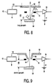
- Figure 8 illustrates the dual electron detector with a relatively long gas path for the primary beam.
- the specimen 58 needs to be placed approximately 1 to 5mm below the collector ring 70 in order to generate adequate amplification of the secondary electron signals.
- the collector ring 70 is positioned approximately 1 to 5mm from the converter plate 52 to obtain sufficient amplification of the backscattered electron signal.
- the primary electron beam has to travel through approximately 2-10mm of gas. This may generate significant beam loss and lead to reduced performance.
- an improved dual electron detector has been designed which shortens the gas path for the primary beam.
- This improved dual detector configuration is illustrated in Figure 9.
- an insulated cone 80 is sealed underneath the converter plate 52.
- the lower opening 81 of the insulated cone 80 forms the pressure limiting aperture which is much closer to the sample.
- the cone 80 must be electrically insulating because of the high voltages that may be present between the detector ring 70 and the converter plate 52.
- the present invention also addresses the effect of the gas path on the primary beam.
- U.S. Pat. No. 5,250,808 previously describes integrating the gaseous detector with a differential pumping system to allow a high vacuum in the electron column even with high gas pressure in the specimen chamber.
- the primary beam passes through the same high pressure gas zone that is used for amplification. This causes some loss of the primary beam due to interaction between the primary beam and the gas. With a 1 to 5mm spacing, the loss is usually acceptable.
- the primary beam has to travel through the gas between the converter plate and the collection plate/grid/ring.
- the sample can advantageously be placed close to the collector grid for the backscattered electron detection since the collector ring is at zero voltage. Therefore, in order to minimize the gas path for the primary beam in the gaseous backscattered electron detector of the present invention, the sample can be placed close to the collection grid and the required gaseous amplification can still be obtained.
- an improved electron detector for an environmental scanning electron microscope which is in the form of a dedicated gaseous detector that is intended to collect only backscattered electron signals.
- This dedicated gaseous detector also causes amplification of the signals to a high enough level to make the noise of the following electronic detectors low.
- the present invention also allows for a simple, low cost, electron detector that can easily be switched between secondary electron detection, backscattered electron detection or both together.
Claims (12)
- Atmosphärisches Rasterelektronenmikroskop mit:dadurch gekennzeichnet, daß die Detektoreinrichtung eine negativ vorgespannte Wandlerplatte (52) aufweist, auf die Rückstreuelektronen (63)auftreffen, die von der Oberfläche der Probe (58) ausgehen, um dadurch Sekundärelektronen an der Oberfläche der Wandlerplatte zu erzeugen, die umgewandelte Rückstreuelektronen bilden.(a) einer Einrichtung zum Erzeugen und Richten eines Elektronenstrahls aus einer Elektronensäule auf eine Probe, die von einer gasförmigen Umgebung in einer Probenkammer eingehüllt ist; und(b) einer Detektoreinrichtung, um nur Rückstreusignale (63) zu detektieren, die von der Probe (58) ausgehen, wobei die Detektoreinrichtung in der gasförmigen Umgebung in der Probenkammer angeordnet ist,
- Atmosphärisches Rasterelektronenmikroskop nach Anspruch 1, wobei die Wandlerplatte eine zentrale Öffnung (50) aufweist, durch die der Elektronenstrahl geht.
- Atmosphärisches Rasterelektronenmikroskop nach Anspruch 2, wobei die zentrale Öffnung der Wandlerplatte eine Enddruckbegrenzungsöffnung zwischen der Elektronensäule und der Probenkammer definiert.
- Atmosphärisches Rasterelektronenmikroskop nach Anspruch 1, wobei die Detektoreinrichtung ferner eine Einrichtung zur Sammlung nur der umgewandelten Rückstreuelektronen aufweist, die durch die Wandlerplatte (66,56,70) erzeugt werden.
- Atmosphärisches Rasterelektronenmikroskop nach Anspruch 4, wobei die Sammeleinrichtung für umgewandelte Rückstreuelektronen in der Form eines Sammelgitters (56) vorliegt, wobei das Sammelgitter mit einem Signalverstärker verbunden ist.
- Atmosphärisches Rasterelektronenmikroskop nach Anspruch 5, wobei das Sammelgitter auf Masse vorgespannt ist, so daß das Gitter nicht die Sekundärelektronen sammelt, die an der Probe erzeugt werden.
- Atmosphärisches Rasterelektronenmikroskop nach Anspruch 4, wobei die Sammeleinrichtung für umgewandelte Rückstreuelektronen eine geteilte Sammelvorrichtung ist, die ein Paar Sammelsegmente aufweist, die symmetrisch um die Elektronenstrahlachse angeordnet sind.
- Atmosphärisches Rasterelektronenmikroskop nach Anspruch 4, wobei die Wandlerplatte und die Sammeleinrichtung für umgewandelte Rückstreuelektronen im Bereich von annähernd 1 bis 5 mm voneinander beabstandet sind.
- Atmosphärisches Rasterelektronenmikroskop nach Anspruch 4, das ferner einen Isolierkegel (80) aufweist, der an einer Unterseite der Wandlerplatte abgedichtet ist und sich von ihr erstreckt und eine Enddruckbegrenzungsöffnung an seinem unteren Ende (81) aufweist, um einen verkürzten Elektronenstrahlweg in der Probenkammer bereitzustellen.
- Atmosphärisches Rasterelektronenmikroskop nach Anspruch 1, wobei die Wandlerplatte mindestens teilweise aus einem Material bestehen kann, das den Wirkungsgrad der Umwandlung der Rückstreuelektronen in Sekundärelektronen erhöht und aus der Gruppe ausgewählt ist, die aus Gold und Magnesiumoxid besteht.
- Atmosphärisches Rasterelektronenmikroskop mit:dadurch gekennzeichnet, daß die Doppeldetektor-Einrichtung eine Wandlerplatte (52) aufweist, die auf eine Spannung V2 vorgespannt ist, auf die Rückstreuelektronen auftreffen, die von der Oberfläche der Probe (58) ausgehen, um dadurch umgewandelte Rückstreuelektronen zu erzeugen, und ferner eine Einrichtung zur Sammlung von Sekundär- und Rückstreuelektronensignalen (70) aufweist, die auf eine Spannung V1 vorgespannt ist und unter der Wandlerplatte (52) in der Probenkammer angeordnet ist, und wobei Vg die Spannung ist, um die erforderliche Verstärkung der Elektronensignale in der gasförmigen Umgebung der Probenkammer zu erhalten, so daß Sekundärelektronensignale nur dann durch die Doppeldetektor-Einrichtung detektiert werden, wenn V1 gleich +Vg ist und V2 gleich +Vg ist, Rückstreuelektronensignale nur dann detektiert werden, wenn V1 0 V und V2 -Vg ist, und sowohl Sekundär- als auch Rückstreuelektronensignale detektiert werden, wenn V1 +Vg ist und V2 zwischen -Vg und +Vg liegt.(a) einer Einrichtung zum Erzeugen und Richten eines Elektronenstrahls (32) aus einer Elektronensäule auf eine Probe (58), die von einer gasförmigen Umgebung in einer Probenkammer (42) eingehüllt ist; und(b) einer Doppeldetektor-Einrichtung zur Detektion von sowohl Sekundärelektronensignalen als auch Rückstreuelektronensignalen, die von der Probe (58) ausgehen, und die zum Umschalten zwischen der Detektion von Sekundärelektronensignalen und Rückstreuelektronensignalen imstande ist, wobei die Detektoreinrichtung in der gasförmigen Umgebung der Probe (58) angeordnet ist,
- Atmosphärisches Rasterelektronenmikroskop nach Anspruch 11, wobei Vg im Bereich von annähernd 100 bis 500 Volt liegt.
Applications Claiming Priority (3)
| Application Number | Priority Date | Filing Date | Title |
|---|---|---|---|
| US15362 | 1998-01-29 | ||
| US09/015,362 US5945672A (en) | 1998-01-29 | 1998-01-29 | Gaseous backscattered electron detector for an environmental scanning electron microscope |
| PCT/IB1999/000056 WO1999039367A1 (en) | 1998-01-29 | 1999-01-18 | Gaseous backscattered electron detector for an environmental scanning electron microscope |
Publications (2)
| Publication Number | Publication Date |
|---|---|
| EP0970503A1 EP0970503A1 (de) | 2000-01-12 |
| EP0970503B1 true EP0970503B1 (de) | 2005-03-23 |
Family
ID=21770969
Family Applications (1)
| Application Number | Title | Priority Date | Filing Date |
|---|---|---|---|
| EP99900089A Expired - Lifetime EP0970503B1 (de) | 1998-01-29 | 1999-01-18 | Gasgefülter rückstrevelektronendetektor für rasterelektronenmikroskop unterkontrollierter umgebung |
Country Status (6)
| Country | Link |
|---|---|
| US (1) | US5945672A (de) |
| EP (1) | EP0970503B1 (de) |
| JP (1) | JP2002516647A (de) |
| AU (1) | AU753825B2 (de) |
| DE (1) | DE69924325T2 (de) |
| WO (1) | WO1999039367A1 (de) |
Families Citing this family (25)
| Publication number | Priority date | Publication date | Assignee | Title |
|---|---|---|---|---|
| IL124333A0 (en) * | 1998-05-05 | 1998-12-06 | El Mul Technologies Ltd | Charges particle detector |
| DE19828476A1 (de) * | 1998-06-26 | 1999-12-30 | Leo Elektronenmikroskopie Gmbh | Teilchenstrahlgerät |
| GB0005717D0 (en) * | 2000-03-09 | 2000-05-03 | Univ Cambridge Tech | Scanning electron microscope |
| FR2806527B1 (fr) | 2000-03-20 | 2002-10-25 | Schlumberger Technologies Inc | Colonne a focalisation simultanee d'un faisceau de particules et d'un faisceau optique |
| AUPQ932200A0 (en) * | 2000-08-11 | 2000-08-31 | Danilatos, Gerasimos Daniel | Environmental scanning electron microscope |
| JP2003068241A (ja) * | 2000-11-08 | 2003-03-07 | Seiko Instruments Inc | 走査型電子線装置 |
| CZ20031455A3 (cs) * | 2000-12-01 | 2003-10-15 | Yeda Research And Development Co. Ltd. | Zařízení a způsob pro zkoumání vzorků v nevakuovém prostředí s použitím skenovacího elektronového mikroskopu |
| DE60118070T2 (de) * | 2001-09-04 | 2006-08-17 | Advantest Corp. | Partikelstrahlgerät |
| ATE524821T1 (de) * | 2002-05-31 | 2011-09-15 | Zeiss Carl Smt Ltd | Verbesserungen in einem teilchendetektor |
| EP1509761A2 (de) | 2002-06-05 | 2005-03-02 | Quantomix Ltd. | Verfahren zur sem-untersuchung von fluidhaltigen proben |
| IL150056A0 (en) * | 2002-06-05 | 2002-12-01 | Yeda Res & Dev | Low-pressure chamber for scanning electron microscopy in a wet environment |
| JP4520303B2 (ja) * | 2002-09-18 | 2010-08-04 | エフ・イ−・アイ・カンパニー | 荷電粒子ビームシステム |
| US20070125947A1 (en) * | 2003-02-20 | 2007-06-07 | David Sprinzak | Sample enclosure for a scanning electron microscope and methods of use thereof |
| JP4636897B2 (ja) | 2005-02-18 | 2011-02-23 | 株式会社日立ハイテクサイエンスシステムズ | 走査電子顕微鏡 |
| WO2007021163A1 (en) * | 2005-08-18 | 2007-02-22 | Cebt Co. Ltd. | Detector for electron column and method for detecting electrons for electron column |
| JP5075375B2 (ja) * | 2006-08-11 | 2012-11-21 | 株式会社日立ハイテクノロジーズ | 走査電子顕微鏡 |
| EP2109873B1 (de) * | 2007-02-06 | 2017-04-05 | FEI Company | Geladenes teilchenstrahlsystem unter hochdruck |
| EP2105944A1 (de) * | 2008-03-28 | 2009-09-30 | FEI Company | "Environmental Cell" für eine TeilchenoptischeVorrichtung |
| US7791020B2 (en) * | 2008-03-31 | 2010-09-07 | Fei Company | Multistage gas cascade amplifier |
| US8299432B2 (en) * | 2008-11-04 | 2012-10-30 | Fei Company | Scanning transmission electron microscope using gas amplification |
| US9679741B2 (en) | 2010-11-09 | 2017-06-13 | Fei Company | Environmental cell for charged particle beam system |
| EP2487703A1 (de) | 2011-02-14 | 2012-08-15 | Fei Company | Detektor zur Verwendung in der Mikroskopie mit geladenen Teilchen |
| EP2518755B1 (de) | 2011-04-26 | 2014-10-15 | FEI Company | In-Column-Detektor für eine teilchenoptische Säule |
| EP2555220A1 (de) | 2011-08-03 | 2013-02-06 | Fei Company | Detektionssystem für geladene Teilchen mit einer Wandlerelektrode |
| EP2682978B1 (de) * | 2012-07-05 | 2016-10-19 | ICT Integrated Circuit Testing Gesellschaft für Halbleiterprüftechnik mbH | Verunreinigungsverringerungselektrode für Partikeldetektor |
Family Cites Families (12)
| Publication number | Priority date | Publication date | Assignee | Title |
|---|---|---|---|---|
| DE2921151C2 (de) * | 1979-05-25 | 1982-12-02 | Ernst Leitz Wetzlar Gmbh, 6330 Wetzlar | Vorrichtung zum Nachweis von in einem Abtast-Elektronenstrahlmikroskop von einer Probe ausgehenden Rückstreuelektronen |
| AU534811B2 (en) * | 1979-07-03 | 1984-02-16 | Unisearch Limited | Atmospheric scanning electron microscope |
| US4720633A (en) * | 1986-01-17 | 1988-01-19 | Electro-Scan Corporation | Scanning electron microscope for visualization of wet samples |
| EP0275306B1 (de) * | 1986-08-01 | 1990-10-24 | Electro-Scan Corporation | Mehrzwecksgasdetektoranordnung fuer elektronmikroskopen |
| US5250808A (en) * | 1987-05-21 | 1993-10-05 | Electroscan Corporation | Integrated electron optical/differential pumping/imaging signal system for an environmental scanning electron microscope |
| US4880976A (en) * | 1987-05-21 | 1989-11-14 | Electroscan Corporation | Secondary electron detector for use in a gaseous atmosphere |
| US4823006A (en) * | 1987-05-21 | 1989-04-18 | Electroscan Corporation | Integrated electron optical/differential pumping/imaging signal detection system for an environmental scanning electron microscope |
| US4785182A (en) * | 1987-05-21 | 1988-11-15 | Electroscan Corporation | Secondary electron detector for use in a gaseous atmosphere |
| US4897545A (en) * | 1987-05-21 | 1990-01-30 | Electroscan Corporation | Electron detector for use in a gaseous environment |
| US4857743A (en) * | 1988-08-04 | 1989-08-15 | Electroscan Corporation | Disposable spray aperture |
| US5412211A (en) * | 1993-07-30 | 1995-05-02 | Electroscan Corporation | Environmental scanning electron microscope |
| US5362964A (en) * | 1993-07-30 | 1994-11-08 | Electroscan Corporation | Environmental scanning electron microscope |
-
1998
- 1998-01-29 US US09/015,362 patent/US5945672A/en not_active Expired - Lifetime
-
1999
- 1999-01-18 JP JP53908599A patent/JP2002516647A/ja active Pending
- 1999-01-18 AU AU17783/99A patent/AU753825B2/en not_active Ceased
- 1999-01-18 EP EP99900089A patent/EP0970503B1/de not_active Expired - Lifetime
- 1999-01-18 DE DE69924325T patent/DE69924325T2/de not_active Expired - Lifetime
- 1999-01-18 WO PCT/IB1999/000056 patent/WO1999039367A1/en active IP Right Grant
Also Published As
| Publication number | Publication date |
|---|---|
| DE69924325D1 (de) | 2005-04-28 |
| EP0970503A1 (de) | 2000-01-12 |
| AU1778399A (en) | 1999-08-16 |
| AU753825B2 (en) | 2002-10-31 |
| JP2002516647A (ja) | 2002-06-04 |
| DE69924325T2 (de) | 2005-09-08 |
| US5945672A (en) | 1999-08-31 |
| WO1999039367A1 (en) | 1999-08-05 |
Similar Documents
| Publication | Publication Date | Title |
|---|---|---|
| EP0970503B1 (de) | Gasgefülter rückstrevelektronendetektor für rasterelektronenmikroskop unterkontrollierter umgebung | |
| EP0444085B1 (de) | Elektronendetektor zur verwendung in einer gasförmigen umgebung | |
| US5828064A (en) | Field emission environmental scanning electron microscope | |
| EP0753200B1 (de) | Rasterelektronenmikroskop in kontrollierter atmosphäre | |
| US4785182A (en) | Secondary electron detector for use in a gaseous atmosphere | |
| EP1022766B1 (de) | Teilchenstrahlgerät | |
| US7541580B2 (en) | Detector for charged particle beam instrument | |
| US8299432B2 (en) | Scanning transmission electron microscope using gas amplification | |
| US4880976A (en) | Secondary electron detector for use in a gaseous atmosphere | |
| AU748781B2 (en) | Environmental SEM with a magnetic field for improved secondary electron detection | |
| KR20010080558A (ko) | 마이크로칼럼에서 효율적인 2차 전자 수집을 위한 검출기구성 | |
| JPH0935679A (ja) | 走査電子顕微鏡 | |
| JPH0982261A (ja) | 電子顕微鏡 | |
| JPH03295141A (ja) | 検出器 |
Legal Events
| Date | Code | Title | Description |
|---|---|---|---|
| PUAI | Public reference made under article 153(3) epc to a published international application that has entered the european phase |
Free format text: ORIGINAL CODE: 0009012 |
|
| AK | Designated contracting states |
Kind code of ref document: A1 Designated state(s): DE FR GB NL |
|
| RBV | Designated contracting states (corrected) |
Designated state(s): DE FR GB NL |
|
| 17P | Request for examination filed |
Effective date: 20000207 |
|
| 17Q | First examination report despatched |
Effective date: 20030217 |
|
| GRAP | Despatch of communication of intention to grant a patent |
Free format text: ORIGINAL CODE: EPIDOSNIGR1 |
|
| GRAS | Grant fee paid |
Free format text: ORIGINAL CODE: EPIDOSNIGR3 |
|
| GRAA | (expected) grant |
Free format text: ORIGINAL CODE: 0009210 |
|
| AK | Designated contracting states |
Kind code of ref document: B1 Designated state(s): DE FR GB NL |
|
| PG25 | Lapsed in a contracting state [announced via postgrant information from national office to epo] |
Ref country code: NL Free format text: LAPSE BECAUSE OF FAILURE TO SUBMIT A TRANSLATION OF THE DESCRIPTION OR TO PAY THE FEE WITHIN THE PRESCRIBED TIME-LIMIT Effective date: 20050323 |
|
| REG | Reference to a national code |
Ref country code: GB Ref legal event code: FG4D |
|
| REF | Corresponds to: |
Ref document number: 69924325 Country of ref document: DE Date of ref document: 20050428 Kind code of ref document: P |
|
| NLV1 | Nl: lapsed or annulled due to failure to fulfill the requirements of art. 29p and 29m of the patents act | ||
| PLBE | No opposition filed within time limit |
Free format text: ORIGINAL CODE: 0009261 |
|
| STAA | Information on the status of an ep patent application or granted ep patent |
Free format text: STATUS: NO OPPOSITION FILED WITHIN TIME LIMIT |
|
| ET | Fr: translation filed | ||
| 26N | No opposition filed |
Effective date: 20051227 |
|
| REG | Reference to a national code |
Ref country code: FR Ref legal event code: PLFP Year of fee payment: 18 |
|
| REG | Reference to a national code |
Ref country code: FR Ref legal event code: PLFP Year of fee payment: 19 |
|
| REG | Reference to a national code |
Ref country code: FR Ref legal event code: PLFP Year of fee payment: 20 |
|
| PGFP | Annual fee paid to national office [announced via postgrant information from national office to epo] |
Ref country code: FR Payment date: 20171211 Year of fee payment: 20 |
|
| PGFP | Annual fee paid to national office [announced via postgrant information from national office to epo] |
Ref country code: DE Payment date: 20180103 Year of fee payment: 20 Ref country code: GB Payment date: 20180117 Year of fee payment: 20 |
|
| REG | Reference to a national code |
Ref country code: DE Ref legal event code: R071 Ref document number: 69924325 Country of ref document: DE |
|
| REG | Reference to a national code |
Ref country code: GB Ref legal event code: PE20 Expiry date: 20190117 |
|
| PG25 | Lapsed in a contracting state [announced via postgrant information from national office to epo] |
Ref country code: GB Free format text: LAPSE BECAUSE OF EXPIRATION OF PROTECTION Effective date: 20190117 |