TECHNICAL FIELD
The present invention relates to an encoding method and
a memory apparatus applicable preferably to a multi-valued
recording flash memory, a memory card using that flash memory
and so on.
BACKGROUND ART
In recent years, as the memory apparatus, semiconductor
memories such as flash memories have been widely used. In the
flash memory, data are recorded by using cell arrays that comprise
a large number of memory cells (numbering usually about 65
million) comprising floating gates (charge storage layer) and
control gates arranged in layered fashion on a semiconductor
substrate (see Fig. 16). In this case, each of the cell arrays
retains data as charge quantities stored in floating gates.
Figs. 17A and 17B illustrate a structure of a memory cell
100 used in a flash memory. That is, the memory cell 100 is so
formed as to stack a charge storage layer (floating gate) 102
and a control gate 103 on a semiconductor substrate 101. When
a data item is to be written to the memory cell 100, the quantity
of charge held in the floating gate 102 is controlled so that
it is reached to one of two threshold voltages shown in Fig. 18
according to the data ("0" or "1") to be recorded. On the other
hand, when the data item is to be read from the memory cell 100,
by using a reference voltage set between the two threshold
voltages, it is determined that the data item in the memory cell
100 is judged to be "0" or "1" depending on whether the threshold
voltage of the memory cell 100 is higher or lower than the
reference voltage.
It is critical to semiconductor memories to prevent
declines in reliability stemming from diverse effects of
high-integration, high-density circuit implementation. As part
of the effort to preserve memory device reliability, an error
correcting circuit based on an error correcting code such as the
Hamming code is often incorporated in the semiconductor memory
in order to counter aging-induced failures such as faulty cells,
resulting in particular from an increasing number of write and
erase operations.
The error correcting code is a redundant code called check
data attached to information data and then the check data are
used to correct an error in the entire code. For example, 10-bit
check data as shown in Fig. 19 are added to an abbreviated Hamming
code for a 512-bit block of information data so that, even if
one error occurs in the 522-bit code, the error may be corrected.
Fig. 20 shows a structure of a flash memory 110
incorporating an error correcting circuit based on the Hamming
code therein. The flash memory 110 comprises cell arrays 111
having a plurality of memory cells, an encoder 112 converting
input data Din into an abbreviated Hamming code to provide write
data WD to be written to the cell arrays 111 and a Hamming code
decoder 113 providing output data Dout by subjecting read data
RD retrieved from the cell arrays 111 to an error correction
process. In this case, the encoder 112 and Hamming code decoder
113 constitute an error correcting circuit. The encoder 112 adds
10-bit check data to every 512-bit block of input data Din and
the abbreviated Hamming code for the 512-bit information data
is created.
In the flash memory 110 shown in Fig. 20, a data write
operation takes place as follows. That is, input data Din are
first inputted to the encoder 112. Then, the encoder 112
converts the input data Din into the abbreviated Hamming code
for 512-bit information data, thereby generating write data WD.
The write data WD outputted from the encoder 112 are fed and
written to the cell arrays 111.
On the other hand, a data read operation is carried out
as follows. Read data RD retrieved from the cell arrays 111 are
inputted to the Hamming code decoder 113. If one code of the
read data RD contains no error, the Hamming code decoder 113
outputs the information data unchanged as output data Dout. If
one code of the read data RD has one erroneous bit, the Hamming
code decoder 113 outputs the information data as the output data
Dout after correcting the error.
Next, an example in which an abbreviated BCH code
(Bose-Chaudhuri-Hocquenghem code) is used as an error correcting
code capable of correcting two errors in one code will be
described. The BCH code and techniques of code abbreviation are
discussed illustratively by Hideki Imai in "Code Theories"
(Institute of Electronics, Information and Communication
Engineers of Japan) among others. For example, 20-bit check data
are added to the abbreviated BCH code for 512-bit information
data as shown in Fig. 21, thereby enabling to correct two errors
in the 532-bit code.
Fig. 22 shows a structure of a flash memory 120
incorporating an error correcting circuit based on the BCH code.
The flash memory 120 comprises cell arrays 121 having a plurality
of memory cells, an encoder 122 for converting input data Din
into an abbreviated BCH code to provide write data WD to be written
to the cell arrays 121 and a BCH code decoder 123 for subjecting
read data RD retrieved from the cell arrays 121 to an error
correction process to provide output data Dout. In this case,
the encoder 122 and the BCH code decoder 123 constitute an error
correcting circuit. The encoder 122 adds 20-bit check data to
every 512-bit block of input data Din and the abbreviated BCH
code capable of correcting two errors regarding the 512-bit
information data is created.
In the flash memory 120 shown in Fig. 22, a data write
operation takes place as follows. That is, input data Din are
first inputted to the encoder 122. Then, the encoder 122
converts the input data Din into the abbreviated BCH code for
512-bit information data, thereby generating write data WD. The
write data WD outputted from the encoder 122 are fed and written
to the cell arrays 121.
On the other hand, a data read operation is carried out
as follows. Read data RD retrieved from the cell arrays 121 is
inputted to the BCH code decoder 123. If one code of the read
data RD contains no error, the BCH code decoder 123 outputs the
information data unchanged as output data Dout. If one code of
the read data RD has one or two erroneous bits, the information
data are outputted as the output data Dout after correcting the
error.
As shown in Figs. 20 and 22, the error correcting circuit
incorporated in the flash memory 110 or 120 can suppress errors
of written data despite a certain number of faulty cells caused
by aging. However, generally in the error correcting code, a
relatively large quantity of the check data, which are redundant
check data, are required to correct a fairly large number of
errors and thus, the number of memory cells to be used is increased
as well as the scale of the error correcting circuit to be
incorporated is enlarged.
Next, a memory card constituted by a plurality of flash
memories (flash memory chips) will be described. As a memory
device for storing quantities of data that cannot be handled by
a single-chip flash memory, the memory card includes multiple
flash memories and a controller.
Fig. 23 shows a structure of a memory card 130 with a
controller having an error correcting circuit based on the BCH
code. The memory card 130 includes two flash memories 131 and
132 and a controller 133 for writing and reading data to and from
these flash memories 131 and 132.
The controller 133 comprises a card interface 134 for
exchanging data with an entity outside the card, an encoder 135
for converting input data Din into an abbreviated BCH code to
provide write data WD to be written to the flash memories 131
and 132, a BCH code decoder 136 for subjecting read data RD from
the flash memories 131 and 132 to an error correction process
to provide output data Dout, and a flash interface 137 for
controlling the writing and reading of data to and from the flash
memories 131 and 132.
In the above structure, the encoder 135 and the BCH code
decoder 136 constitute an error correcting circuit. The encoder
135 adds 20-bit check data to every 512-bit block of input data
Din, thus creating an abbreviated BCH code capable of correcting
two errors regarding the 512-bit information data.
In the memory card 130 shown in Fig. 23, a data write
operation takes place as follows. That is, input data Din are
first taken into the card by the card interface 134 and supplied
to the encoder 135. Then, the encoder 135 converts the input
data Din into the abbreviated BCH code for 512-bit information
data, thereby generating write data WD. The write data WD
outputted from the encoder 135 are written to the flash memory
131 or 132 under control of the flash interface 137.
On the other hand, a data read operation is carried out
as follows. Read data RD retrieved from the flash memory 131
or 132 under control of the flash interface 137 are inputted to
the BCH code decoder 136. If one code of the read data RD contains
no error, the BCH code decoder 136 outputs the information data
unchanged as output data Dout. If one code of the read data RD
has one or two erroneous bits, the BCH code decoder 136 outputs
the information data as the output data Dout after correcting
the error(s). In this way, the output data Dout are outputted
from the BCH code decoder 136 to an entity outside the card via
the card interface 134.
As described above, the error correcting code is also used
in a memory card made of a plurality of flash memories. If a
controller is used for error correction, it is possible to have
a characteristic that error correcting circuit larger than an
error correcting circuit incorporated in the flash memory is
obtained so that the greater number of errors may be corrected.
Next, multi-value recording of a flash memory will be
described. In recent years, flash memories are proposed for
multi-bits recording per cell in an effort to increase storage
capacity of the flash memory. For example, as shown in Figs. 24A
through 24D, the quantity of charge accumulated in a floating
gate 102 in a memory cell 100 of a flash memory for four-value
recording is controlled so that it may attain one of four
threshold voltages shown in Fig. 25 representing a data item to
be stored ("11," "10," "01" or "00"). When data are read, three
reference voltages each established between the respective
adjacent threshold values are used. By comparing the threshold
value in the memory cell 100 with each of the reference voltages,
the data from the memory cell 100 are retrieved. This arrangement
allows each memory cell 100 to store two-bit information.
Multi-value recording flash memories may, as with their
binary recording counterparts, utilize an error correcting
circuit as well. Fig. 26 shows a structure of a flash memory 140
for 16-value (4-bit) recording incorporating an error correcting
circuit based on the BCH code. The flash memory 140 comprises
cell arrays 141 having a plurality of memory cells, an encoder
142 for converting input data Din into an abbreviated BCH code
to provide write data WD to be written to the cell arrays 141
and a one-bit/four-bit converter 143 for converting write data
WD outputted from the encoder 142 from serial data format to
four-bit parallel data format and supplying the converted data
to the cell arrays 141.
The flash memory 140 also includes a four-bit/one-bit
converter 144 for converting read data RD retrieved from the cell
arrays 141 from four-bit parallel data format to serial data
format and a BCH code decoder 145 for providing output data Dout
by subjecting to an error correction process the read data RD
converted to serial data by the four-bit/one-bit converter 144.
In this case, the encoder 142 and the BCH code decoder 145
constitute an error correcting circuit. The encoder 142 adds
20-bit check data to every 512-bit block of input data Din,
thereby creating an abbreviated BCH code capable of correcting
two errors regarding the 512-bit information data.
In the flash memory 140 shown in Fig. 26, a data write
operation takes place as follows. That is, input data Din are
first inputted to the encoder 142. Then, the encoder 142 converts
the input data Din into the abbreviated BCH code for 512-bit
information data, thereby generating write data WD. The write
data WD outputted from the encoder 142 are converted by the
one-bit/four-bit converter 143 from serial data format to
four-bit parallel data format (four-bit data for storage into
memory cells), thus supplying the write data WD to the cell arrays
141 and writing the data WD consecutively to each of memory cells
making up the cell arrays 141.
On the other hand, a data read operation is carried out
as follows. Read data RD retrieved from cell arrays 141 are
converted by the four-bit/one-bit converter 144 from four-bit
parallel data format to serial data format. The converted serial
data are supplied to the BCH code decoder 145. If one code of
the read data RD contains no error, the BCH code decoder 145
outputs the information data unchanged as output data Dout. If
one code of the read data RD has one or two erroneous bits, the
BCH code decoder 145 outputs the information data as the output
data Dout after correcting the error(s).
The multi-value recording flash memories such as the flash
memory 140 shown in Fig. 26 have such a characteristic that a
single faulty cell causes multiple erroneous bits. Since
conventional flash memories have stored one bit per memory cell,
these memories principally have used code systems for bit error
correction as their error correcting code. However, if a single
faulty memory cell results in a plurality of erroneous bits, the
error correcting code for bit-by-bit error correction is
inefficient.
For example, in a flash memory wherein each memory stores
four bits of data, if a single memory cell is found inaccessible,
four correcting codes have to be used to correct this error. As
described above, if the above error correcting code is used to
correct many such errors, a large error correcting circuit is
needed so that this causes a disadvantage of an expanded scale
of the error correcting circuit. Because an increasing amount
of redundant data needs to be added in order to correct many errors,
numerous memory cells are required, which poses another
disadvantage.
It is therefore an object of the present invention to
provide a memory apparatus having an error correcting circuit
of a small scale and a limited number of memory cells, wherein
it may maintain sufficient performance by a small number of
correcting errors. It is another object of the present invention
to provide an encoding method and a memory apparatus using that
method, whereby the length of a code is extended while data
exchanges with an outside entity are still carried out, for
example, in units of bytes.
DISCLOSURE OF INVENTION
In carrying out the invention and according to one aspect
thereof, there is provided a memory apparatus comprising cell
arrays having a plurality of memory cells each storing multi-bit
information, an encoder for converting input data into a
Reed-Solomon code to provide write data to be written to the cell
arrays and a Reed-Solomon code decoder for subjecting read data
retrieved from the cell arrays to an error correction process
to provide output data.
According to another aspect of the invention, there is
provided a memory apparatus comprising a memory portion having
cell arrays made of a plurality of memory cells each storing
multi-bit data and a controller for writing and reading data to
and from the memory portion wherein the controller includes an
encoder for converting input data into a Reed-Solomon code to
provide write data to be written to the memory portion and a
Reed-Solomon code decoder for subjecting read data retrieved
from the memory portion to an error correction process to provide
output data.
With the present invention, each memory cell of the cell
arrays stores multi-bit data. For a write operation, the encoder
converts input data into a Reed-Solomon code as write data to
be written to the cell arrays. The Reed-Solomon code reckons
a plurality of bits as one byte and is an error correction code
used for error correction in units of bytes. For a read operation,
multi-bit data are read from each memory cell of the cell arrays
and the read data are subjected to an error correction process
by the Reed-Solomon code decoder, thereby providing output data.
In this way, the Reed-Solomon code for error correction
in units of bytes is thus used as the error correcting code for
the memory apparatus made of memory cells each storing multi-bit
data so that it is possible to provide sufficient performance
involving a limited number of correcting errors. This makes it
possible to reduce the error correcting circuit in scale with
a smaller number of memory cells to be used than before.
Further, according to a further aspect of the invention,
there is provided an encoding method comprising the steps of
supplementing (n-m) bit data with m-bit data for conversion into
n-bit data, n being greater than m, encoding the n-bit data using
a Reed-Solomon code reckoning n bits as one symbol, and outputting
as information data the m-bit data before supplementing the (n-m)
bit data while outputting as check data the m-bit data after
having undergone n-bit/m-bit conversion.
Further, according to an even further aspect of the
invention, there is provided a memory apparatus comprising cell
arrays having a plurality of memory cells, an encoder for
converting input data into an error correcting code to provide
write data to be written to the cell arrays, and a decoder for
subjecting read data retrieved from the cell arrays to an error
correction process to provide output data, characterized in that
the encoder supplements (n-m) bit data with m-bit input data for
conversion into n-bit data, n being greater than m, encodes the
n-bit data using a Reed-Solomon code reckoning n bits as one
symbol and outputs as information data the m-bit data before
supplementing the (n-m) bit data while outputting as check data
the m-bit data after having undergone n-bit/m-bit conversion and
that the decoder supplements the (n-m) bit data relating to an
information data part thereof with the m-bit read data retrieved
from the cell arrays for conversion into n-bit data, subjects
a check data part to m-bit/n-bit conversion into n-bit data,
thereafter submits the converted n-bit data to an error
correction process and provides as the output data an m-bit data
part in the corrected n-bit information data.
Further, according to a still further aspect of the
invention, there is provided a memory apparatus comprising a
memory portion having cell arrays made of a plurality of memory
cells and a controller for writing and reading data to and from
the memory portion, characterized in that the controller
includes an encoder for converting input data into an error
correcting code to provide write data to be written to the memory
portion, and a decoder for subjecting read data retrieved from
the memory portion to an error correction process to provide
output data, wherein the encoder supplements (n-m) bit data with
m-bit input data for conversion into n-bit data, n being greater
than m, encodes the n-bit data using a Reed-Solomon code reckoning
n bits as one symbol and outputs as information data the m-bit
data before supplementing the (n-m) bit data while outputting
as check data the m-bit data after having undergone n-bit/m-bit
conversion, and wherein the decoder supplements the n-m bit
data with m-bit read data retrieved from the cell arrays for
conversion into n-bit data relating to an information data part
thereof, subjects a check data part of the m-bit read data to
m-bit/n-bit conversion into n-bit data, thereafter submits the
converted n-bit data to an error correction process and provides
as the output data an m-bit data part in the corrected n-bit
information data.
With the present invention, each memory cell of the cell
arrays stores data of one bit or plural bits. For a write
operation, m-bit input data are inputted to the encoder. The (n-m)
bit data (n > m) of, for example, 0 are supplemented with m-bit
input data for conversion into n-bit data. For example,
eight-bit input data are supplemented with two-bit zeros for
conversion into 10-bit data. The n-bit data are then converted
to a Reed-Solomon code reckoning n bites as one symbol. The m-bit
data before supplementing the (n-m) bit data are outputted as
information data, while the m-bit data after having undergone
n-bit/m-bit conversion are outputted as check data. Then, the
m-bit data outputted from the encoder are fed and written
successively to cells of the cell arrays.
The Reed-Solomon code is an error correcting code that
reckons a plurality of bits as one symbol for error correction
in units of symbols. For a read operation, the m-bit data
retrieved from the cell arrays are inputted to the decoder. Then,
the (n-m) bit data are supplemented with the m-bit data for an
information data part thereof for conversion into n-bit data,
and a check data part thereof is subjected to m-bit/n-bit
conversion into n-bit data, whereby the Reed-Solomon code
reckoning n bits as one symbol is reconstituted. Next, the
reconstituted Reed-Solomon code is subjected to an error
correction process. Then, an m-bit part of the corrected n-bit
information data is outputted as the output data.
As described above, the input and the output data are both
m-bit data whereas the encoder uses for its encoding operation
the Reed-Solomon code reckoning n bits (n > m) as one symbol.
Therefore, this makes it possible to extend the code length while
maintaining data exchanges with an external entity in units of
m bits. For this reason, there is no need to divide information
data of a predetermined length into segments for encoding
purposes. This makes it possible to reduce check data (redundant
data) while preserving the continuity of decoded data.
BRIEF DESCRIPTION OF DRAWINGS
Fig. 1 is a block diagram of a flash memory practiced as
a first embodiment of this invention;
Fig. 2 is a schematic view of a typical abbreviated
Reed-Solomon code;
Fig. 3 is an explanatory view showing how bit conversion
takes place;
Fig. 4 is a block diagram of a memory card practiced as
a second embodiment of the invention;
Fig. 5 is an explanatory view depicting how data are read
from a cell array;
Fig. 6 is a schematic view of four abbreviated Reed-Solomon
codes permitting correction of one error in 512-byte
information data;
Fig. 7 is an explanatory view illustrating the continuity
of decoded data;
Fig. 8 is a block diagram of a structure of flash memory
practiced as a third embodiment of the invention;
Fig. 9 is a block diagram of a structure of an encoder
in the flash memory;
Fig. 10 is an explanatory view depicting an operation of
eight-bit/10-bit conversion of an information data part upon
encoding and decoding;
Fig. 11 is an explanatory view showing an operation of
eight-bit/10-bit conversion of a check data part upon encoding
and decoding;
Fig. 12 is a block diagram showing a structure of a decoder
in the flash memory;
Fig. 13 is an explanatory view illustrating an operation
of 10-bit/eight-bit conversion upon decoding;
Fig. 14 is an explanatory view depicting the continuity
of decoded data;
Fig. 15 is a block diagram showing a structure of a memory
card practiced as a fourth embodiment of the invention;
Fig. 16 is a schematic view showing a structure of a cell
array;
Figs. 17A and 17B are schematic views showing a structure
of a memory cell;
Fig. 18 is a graphic representation showing voltage
distribution in memory cells;
Fig. 19 is a schematic view of a typical abbreviated
Hamming code;
Fig. 20 is a block diagram showing a structure of a flash
memory incorporating an error correcting circuit based on the
abbreviated Hamming code;
Fig. 21 is a schematic view of a typical abbreviated BCH
code;
Fig. 22 is a block diagram showing a structure of a flash
memory incorporating an error correcting circuit based on the
BCH code;
Fig. 23 is a block diagram showing a structure of a memory
card with a controller incorporating an error correcting circuit
based on the abbreviated BCH code;
Figs. 24A through 24D are schematic views showing how a
memory cell is electrically charged for multi-value recording;
Fig. 25 is a graphic representation illustrating voltage
distribution in memory cells for multi-value recording; and
Fig. 26 is a block diagram showing a structure of a
multi-value recording flash memory incorporating an error
correcting circuit based on the abbreviated BCH code.
BEST MODE FOR CARRYING OUT THE INVENTION
Fig. 1 shows a structure of a flash memory 10 practiced
as the first embodiment of the invention. The flash memory 10
designed for 16-value (4-bit) recording incorporates an error
correcting circuit based on the abbreviated Reed-Solomon code
capable of double-error correction. Each of the Reed-Solomon
code and the abbreviated Reed-Solomon code reckons a plurality
of bits as one byte to correct error in a unit of byte. Details
of the Reed-Solomon code are described illustratively in the
above-cited publication "Code Theories" by Hideki Imai
(Institute of Electronics, Information and Communication
Engineers of Japan) among others.
Now, consider an abbreviated Reed-Solomon code reckoning
eight bits as one byte to correct two errors in 128-byte
information data. In this case, as shown in Fig. 2, check data
are made of four bytes and the code as a whole is 132 bytes long
(=1056 bits).
In Fig. 1, the flash memory 10 comprises cell arrays 11
having a plurality of memory cells, an encoder 12 for converting
eight-bit parallel input data Din into an abbreviated Reed-Solomon
code to provide write data WD to be written to the cell
arrays 11 and an eight-bit/four-bit converter 13 for converting
one-byte (8-bit) parallel write data WD outputted by the encoder
12 into four-bit parallel data (four-bit data to be stored in
memory cell) that are fed to the cell arrays 11, as shown in Fig.
3.
The flash memory 10 further includes a four-bit/eight-bit
converter 14 for converting four-bit parallel read data RD
retrieved from the cell arrays 11 into one-byte (8-bit) parallel
data as shown in Fig. 3, and a Reed-Solomon code decoder 15 for
subjecting read data RD converted as one-byte parallel data in
the four-bit/eight-bit converter 14 to an error correction
process to provide output data Dout. In this structure, the
encoder 12 and the Reed-Solomon code decoder 15 constitute an
error correcting circuit. Then, the encoder 12 supplements each
128-byte block of input data Din with four-byte check data to
generate an abbreviated Reed-Solomon code for correcting two
errors in the 128-byte block of information data.
In the flash memory 10 shown in Fig. 1, a data write
operation is carried out as follows. That is, eight-bit parallel
input data Din are inputted to the encoder 12. Then, the encoder
12 converts the input data Din into an abbreviated Reed-Solomon
code for 128 bytes of information data to provide write data WD.
The one-byte (8-bit) parallel write data WD outputted by the
encoder 12 are converted by the eight-bit/four-bit converter 13
into four-bit parallel data to be fed to the cell arrays 11 so
that the converted data are written consecutively to memory cells
making up the cell arrays 11.
On the other hand, a data read operation takes place as
follows. Four-bit parallel read data RD retrieved from the cell
arrays 11 are converted by the four-bit/eight-bit converter 14
into one-byte (8-bit) parallel data that are supplied to the
Reed-Solomon code decoder 15. If one code of read data RD has
no error, the Reed-Solomon code decoder 15 outputs information
data unchanged as output data Dout in units of bytes. If one code
of the read data RD has one or two erroneous bytes, the
Reed-Solomon code decoder 15 outputs information data as the
output data Dout in units of bytes after correcting the error(s).
If the input data Din or output data Dout are not eight-bit
parallel data, a bit converter may be furnished upstream of the
encoder 12 to convert the input data Din into eight-bit parallel
data, or a bit converter may be installed downstream of the
Reed-Solomon code decoder 15 to convert the eight-bit parallel
data into parallel or serial data representing the output data
Dout.
In the first embodiment, the Reed-Solomon code is employed
as an error correcting code for correcting errors in units of
bytes in the cell arrays 11 made of memory cells each storing
four-bit data and then sufficient performance may be attained
with a limited number of correcting errors. Therefore, this
makes it possible to reduce the error correcting circuit in scale
and make smaller a number of memory cells to be used.
Effects of the first embodiment are illustrated below.
For purposes of illustration, it is assumed that 65,536
information data cells constitute one block and 1,024 blocks make
up a cell array, and that data are written and read to and from
the memory in units of blocks. It is also assumed that the
probability of a normally fabricated cell becoming faulty
(inaccessible) after one million write/erase operations is
0.001% and further, on these assumptions, the probability of a
block becoming faulty after one million write/erase operations
is compared.
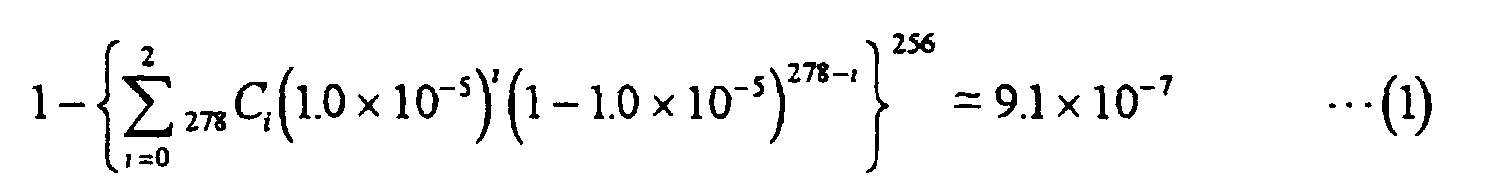
Where the abbreviated BCH code is used for the correction
of up to eight erroneous bits in 128 bytes, that is, 1,024-bit
information data, 88 bits of check data are needed. Since one
defective cell requires the correction of four bits, this error
correcting code for eight-error correction permits correction
of up to two faulty cells. Since 1,112 bits are stored in 278
cells and one block contains 256 codes, the probability of a block
getting faulty is about 0.000091% as calculated by the expression
(1) below.
Next, the probability of a block becoming faulty is then
acquired when the abbreviated Reed-Solomon code for double-error
correction is used. In this case, errors of up to two bytes can
be corrected. Here, when it is taken into account that a
single-cell error will not affect multiple bytes according to
the four-bit/eight-bit conversion, the byte error rate is
defined by the expression (2) below with eight bits of two-cell
information regarded as one byte. Thus, from the ensuing
expression (3), the probability of a block getting defective is
estimated at about 0.000077%.
1-(1-1.0 × 10⁻⁵)2 ≃ 2.0 × 10⁻⁵
Therefore, it will be appreciated that the abbreviated
BCH code for eight-error correction and the abbreviated
Reed-Solomon code for two-error correction have approximately
the same error correcting capability. However, since two errors
for correction by the Reed-Solomon code are much smaller opposed
to eight errors for correction by the BCH code, use of Reed-Solomon
code allows a scale of error correcting circuit to be
composed as a far smaller one than that of BHC code. In addition,
since 32 bits of redundant data for the Reed-Solomon code are
much smaller with compared with 88 bits of redundant data for
the BCH code, a far smaller number of memory cells can be used
therefor.
Next, the second embodiment of this invention will now
be described. Fig. 4 depicts a structure of a memory card 20
practiced as the second embodiment of the invention. The memory
card 20 comprises two flash memories for 16-value (4-bit)
recording and a controller incorporating an error correcting
circuit based on the abbreviated Reed-Solomon code for
double-error correction.
As shown in Fig. 4, the memory card 20 includes two flash
memories 21 and 22 as well as a controller 23 for writing and
reading data to and from the flash memories 21 and 22.
Further, the controller 23 has a card interface 24 for
exchanging data with an entity outside the card, an encoder 25
for converting eight-bit parallel input data Din into an
abbreviated Reed-Solomon code to provide write data WD to be
written to the flash memories 21 and 22, and an eight-bit/four-bit
converter 26 for converting the write data WD of one-byte (8-bit)
parallel data outputted by the encoder 25 into four-bit parallel
data (four-bit data to be stored in memory cells) as depicted
in Fig. 3.
The controller 23 further comprises a four-bit/eight-bit
converter 27 for converting four-bit parallel read data RD
retrieved from the flash memory 21 or 22 into one-byte (8-bit)
parallel data as shown in Fig. 3, a Reed-Solomon code decoder
28 for subjecting to an error correction process the one-byte
parallel read data RD converted in the four-bit/eight-bit
converter 27 to provide output data Dout, and a flash interface
29 for controlling the writing and reading of data to and from
the flash memories 21 and 22.
In the above structure, the encoder 25 and the Reed-Solomon
code decoder 28 constitute an error correcting circuit.
Then, the encoder 25 supplements each 128-byte block of input
data Din with four-byte check data to generate an abbreviated
Reed-Solomon code for correcting two errors in the 128-byte
information data.
In the memory card 20 shown in Fig. 4, a data write
operation is carried out as follows. That is, input data Din
is taken into the card through the card interface 24 and sent
to the encoder 25. The encoder 25 converts the input data Din
into an abbreviated Reed-Solomon code for 128 bytes of
information data to provide write data WD. Then, the eight-bit/four-bit
converter 26 converts the one-byte (8-bit) parallel
write data WD outputted by the encoder 25 into four-bit parallel
data. The converted four-bit parallel data are written to the
flash memory 21 or the flash memory 22 under control of the flash
interface 29.
On the other hand, a data read operation takes place as
follows. Four-bit parallel read data RD retrieved from the flash
memory 21 or the flash memory 22 under control of the flash
interface 29 are converted by the four-bit/eight-bit converter
27 into one-byte (8-bit) parallel data. The converted one-byte
parallel data are fed to the Reed-Solomon code decoder 28. If
one code of read data RD has no error, the Reed-Solomon code
decoder 28 outputs information data unchanged as output data Dout
in units of bytes. If one code of the read data RD has one or
two erroneous bytes, the Reed-Solomon code decoder 28 outputs
information data as the output data Dout in units of bytes after
correcting the error(s). In this way, the output data Dout
outputted by the Reed-Solomon code decoder 28 are sent out of
the card through the card interface 24.
If the input data Din or output data Dout are not eight-bit
parallel data, a bit converter may be furnished upstream of the
encoder 25 to convert the input data Din into eight-bit parallel
data, or a bit converter may be installed downstream of the
Reed-Solomon code decoder 28 to convert the eight-bit parallel
data into parallel or serial data representing the output data
Dout.
As described, in the second embodiment, the Reed-Solomon
code is employed as the error correcting code for error correction
in units of bytes in the flash memories 21 and 22, which constitute
a memory portion, made of cell arrays comprising memory cells
each storing four-bit data. As with the first embodiment, the
second embodiment provides sufficient performance involving a
limited number of errors to be corrected. Accordingly, the
second embodiment also makes it possible to reduce the error
correcting circuit in scale with a smaller number of memory cells
incorporated. Further, since the controller 23 corrects errors,
the error correcting circuit is allowed to be larger in scale
than if the error correcting circuit is incorporated in the flash
memory 21 or 22. Therefore, even if a large number of errors
result from multi-value recording, they can be corrected.
Here, the process of reading data from a flash memory is
recapitulated below. Data are read not in units of cells but
in units called pages (e.g., each page representing 1,024 cells)
simultaneously from cell arrays (see Fig. 16). The read data
are outputted consecutively from an output buffer (see Fig. 5).
Therefore, for example, from a 16-value recording flash memory
where one page represents 1,024 cells of information, 4,096 bits
(512 bytes) of information are retrieved as a unit. Since data
exchanges with an entity outside the memory are carried out mostly
in units of bytes (8 bits), one symbol of the Reed-Solomon code
should preferably be eight bits long so as to ensure consistency.
However, the Reed-Solomon code reckoning eight bits as
one symbol has a code length of 255 bytes and then, this makes
it necessary upon encoding to divide 512-byte data into three
or four segments each supplemented with check data (redundant
data). Fig. 6 shows a state of coding wherein 512-byte data are
encoded illustratively by four abbreviated Reed-Solomon codes
each capable of correcting one error in 128 bytes of information
data.
As a general characteristic of the error correcting code,
performance is better when information data as a whole are encoded,
if supplemented with same number of check data, than when the
same information data are segmented before being coded. Where
512 bytes of information data are to be read out simultaneously,
efficiency is higher if all 512-byte information data are encoded
as a whole.
Further, if data of one page are divided into segments
when encoded, the decoded data are outputted with intervening
blanks when decoded (see Fig. 7). From a system performance point
of view, decoded data of one page should be outputted
uninterrupted as much as possible. Therefore, in that respect,
it is also preferable for data of one page to be encoded as one
block.
Next, the third embodiment of this invention will be
described. Fig. 8 shows a structure of a flash memory 30
practiced as the third embodiment of the invention. The flash
memory 30 permits data exchanges with an outside entity in units
of bytes (8 bits). This flash memory 30 for 16-value (4-bit)
recording incorporates an error correcting circuit based on the
abbreviated Reed-Solomon code capable of double-error
correction.
In this case, since information data, e.g., 512 bytes,
in each page are encoded as one block, encoding is performed using
the abbreviated Reed-Solomon code reckoning 10 bits as one symbol.
Here, if information data of one page are made of 512 bytes, the
check data (redundant data) for double-error correction comprise
four symbols requiring a 516-byte code length. Since the
Reed-Solomon code reckoning 10 bits as one symbol is 1,023 bytes
long, the 516-byte-long code is made available through
abbreviation. Further, the check data comprising four symbols
amounts to 40 bits representing five bytes.
As shown in Fig. 8, the flash memory 30 includes cell
arrays 31 having a plurality of memory cells, an encoder 32 for
converting eight-bit parallel input data Din into an abbreviated
Reed-Solomon code to provide write data WD to be written to the
cell arrays 31, and an eight-bit/four-bit converter 33 for
converting eight-bit write data WD outputted by the encoder 32
into four-bit data (four-bit data to be stored in memory cells)
that are supplied to the cell arrays 31, as shown in Fig. 3.
Further, the flash memory 30 comprises a four-bit/eight-bit
converter 34 for converting four-bit read data RD
retrieved from the cell arrays 31 into eight-bit data as shown
in Fig. 3, and a decoder 35 for subjecting to an error correction
process the eight-bit read data RD converted in the four-bit/eight-bit
converter 34 to provide output data Dout. In this
structure, the encoder 32 and the decoder 35 constitute an error
correcting circuit.
Fig. 9 shows a structure of the encoder 32. The encoder
32 includes an eight-bit/10-bit converter 32a for converting
eight-bit data as input data Din into 10-bit data by supplementing
them with two-bit zeros as shown in Fig. 10, and a Reed-Solomon
encoder 32b for encoding 10-bit data outputted by the converter
32a by use of the Reed-Solomon code reckoning 10 bits as one symbol.
The Reed-Solomon encoder 32b supplements each 512-symbol block
of 10-bit data with four-symbol check data (redundant data) to
generate an abbreviated Reed-Solomon code capable of correcting
two errors in 512 symbols.
Further, the encoder 32 comprises a 10-bit/eight-bit
converter 32c for removing two bits from 10-bit data for
conversion into eight-bit data, a 10-bit/eight-bit converter 32d
for changing the bit configuration of 10-bit data for conversion
into eight-bit data as shown in Fig. 11, a changeover switch 32e
for selectively supplying to the converters 32c and 32d the
512-symbol information data and four-symbol check data
constituting each Reed-Solomon code outputted by the Reed-Solomon
encoder 32b, and a changeover switch 32f for selectively
outputting as write data WD the eight-bit data corresponding to
the 512-symbol information data from the converter 32c and the
eight-bit data corresponding to the four-symbol check data from
the converter 32d. When supplied with the 512-symbol information
data, the converter 32c outputs 512-byte data making up an
information data part. On the other hand, when supplied with
the four-symbol check data, the converter 32d outputs five-byte
data forming a check data part.
Operation of the encoder 32 of the above-described
constitution will be described. Eight-bit input data Din of
eight-bit data are fed to the eight-bit/10-bit converter 32a
wherein the eight-bit data are supplemented with two-bit zeros
for conversion into 10-bit data. Then, such the 10-bit data are
supplied to the Reed-Solomon encoder 32b and converted into an
abbreviated Reed-Solomon code for correcting two errors in the
512-symbol information data.
Of each 516-symbol Reed-Solomon code from the Reed-Solomon
encoder 32b, the 512-symbol information data are sent
to the 10-bit/eight-bit converter 32c, through the changeover
switch 32e, wherein the two-bit zeros added by above-described
eight-bit/10-bit converter 32a are removed from the supplied
10-bit data for conversion into eight-bit data (see Fig. 10).
Then, the resulting eight-bit data are outputted as write data
WD via the changeover switch 32f.
On the other hand, of each 516-symbol Reed-Solomon code
outputted from the Reed-Solomon encoder 32b, the four-symbol
check data are fed to the 10-bit/eight-bit converter 32d, through
the changeover switch 32e, wherein the bit configuration of the
check data is changed for conversion into eight-bit data (see
Fig. 11). Then, the converted eight-bit data are outputted as
write data WD via the changeover switch 32f.
Fig. 12 shows a structure of the decoder 35. The decoder
35 comprises an eight-bit/10-bit converter 35a for supplementing
eight-bit data with two-bit zeros for conversion into 10-bit data
as shown in Fig. 10, an eight-bit/10-bit converter 35b for
changing the bit configuration of eight-bit data for conversion
into 10-bit data as shown in Fig. 11, a changeover switch 35c
for selectively supplying each 512-byte information data part
and each five-byte check data part of eight-bit read data RD
outputted from the four-bit/eight-bit converter 34 (in Fig. 8)
to the converters 35a and 35b, and a changeover switch 35d for
selectively extracting the 10-bit data corresponding to the
512-byte information data part outputted by the converter 35a
and the 10-bit data corresponding to the five-byte check data
part outputted by the converter 35b so as to reconstitute the
abbreviated Reed-Solomon code for correcting two errors in the
512-symbol information data.
Further, the decoder 35 includes a Reed-Solomon code
decoder 35e for subjecting to an error correction process the
Reed-Solomon code outputted by the changeover switch 35d, and
a 10-bit/eight-bit converter 35f for removing two bits from the
10-bit information data having undergone error correction by the
decoder 35e, for conversion into eight-bit data to provide output
data Dout, as shown in Fig. 13.
Operation of the decoder 35 of the above-described
constitution will be described. Of the eight-bit data provided
as the read data RD, each 512-byte information data part is
supplied to the eight-bit/10-bit converter 35a wherein two-bit
zeros are added to the supplied data for conversion into 10-bit
data (see Fig. 10). On the other hand, of the eight-bit data
furnished as the read data RD, each five-byte check data part
is supplied to the eight-bit/10-bit converter 35b wherein the
bit configuration of the supplied data is changed for conversion
into 10-bit data (see Fig. 11).
Then, the changeover switch 35d selectively extracts the
10-bit data corresponding to the 512-byte information data part
outputted by the converter 35a and the 10-bit data corresponding
to the five-byte check data part outputted by the converter 35b,
so that the abbreviated Reed-Solomon code for correcting two
errors in the 512-symbol information data may be reconstituted.
Further, the Reed-Solomon code outputted by the
changeover switch 35d is supplied to the Reed-Solomon code
decoder 35e. If one code contains one or two erroneous symbols,
the Reed-Solomon code decoder 35e corrects the error(s). After
the error correction by the decoder 35e, the 10-bit data as
information data are supplied to the 10-bit/eight-bit converter
35f wherein two bits are removed from the supplied data for
conversion into eight-bit data (see Fig. 13) to provide output
data Dout.
In the flash memory 30 shown in Fig. 8, a data write
operation is carried out as follows. That is, one-byte (8-bit)
input data Din are fed to the encoder 32. Then, the encoder 32
adds two-byte zeros to the input data Din for conversion into
10-bit data. The 10-bit data are converted to a Reed-Solomon
code capable of correcting two errors in 512-symbol information
data. The eight-bit data before supplementing with 0 are
outputted as information data, while the eight-bit data after
the change of the bit configuration are outputted as check data.
Then, the eight-bit write data WD outputted by the encoder 32
are converted by the eight-bit/four-bit converter 33 into
four-bit data and fed to the cell arrays 31. The supplied
four-bit data are written successively to memory cells making
up the cell arrays 31.
On the other hand, a data read operation takes place as
follows. Four-bit read data RD retrieved from the cell arrays
31 are converted by the four-bit/eight-bit converter 34 into
eight-bit data that are fed to the decoder 35. Given the
eight-bit data, the decoder 35 adds two-bit zeros to each 512-byte
information data part for conversion into 10-bit data; each
five-byte check data part has its bit configuration changed for
conversion from eight-bit to 10-bit data. This reconstitutes
the Reed-Solomon code capable of correcting two errors in the
512-symbol information data. Furthermore, the decoder 35
subjects the reconstituted Reed-Solomon code to an error
correction process. From the corrected information data, two
bits are removed for conversion into eight-bit data that are
outputted as the output data Dout in units of bytes.
With the third embodiment, as described, the input data
Din and the output data Dout are eight-bit data and the encoder
32 performs its encoding operation using the Reed-Solomon code
reckoning 10 bits as one symbol and thus, this makes it possible
to extend the code length while maintaining data exchanges with
an external entity in units of one byte (8 bits). Accordingly,
there is no need to divide, for example, 512-byte information
data making up each page into segments for encoding purposes.
The scheme makes it possible to reduce check data (redundant data)
while preserving the continuity of each page of 512-byte decoded
data as shown in Fig. 14.
Effects of the third embodiment are illustrated below.
It is assumed that 65,536 information data cells (i.e., 64 pages)
constitute one block and 1,024 blocks make up a cell array and
it is assumed that even a single error in a block triggers
suppression of access to that block regarded as defective. Now,
it is assumed that the probability of a normally fabricated cell
becoming faulty (inaccessible) after one million write/erase
operations is 0.001%. On these assumptions, the probability of
a block becoming faulty after one million write/erase operations
is compared.
Where the abbreviated Reed-Solomon code is used for
double-error correction in a 512-byte information data part,
with five-byte check data (redundant data) added to the data part
as in the third embodiment, the probability of a faulty block
becoming a reality is obtained. In this case, one abbreviated
Reed-Solomon code can correct up to two symbols. If eight-bit
information corresponding to two cells is regarded as one symbol,
the rate of a symbol getting erroneous is given by the expression
(4) below. The symbol error rate thus furnished is that of
information data. The symbol error rate of check data (redundant
data) is about 2.5 times the rate of a cell getting faulty, i.e.,
2.5 x 10⁻⁵.
1-(1-1.0 × 10⁻⁵)2 ≃ 2.0 × 10⁻⁵
Further, the total number of symbols is 516, and one block
contains 64 codes. Because the symbol error rate of check data
is higher than that of information data, the probability of a
block becoming defective is evaluated through the use of the
symbol error rate regarding check data. Accordingly, the
probability of a faulty block becoming a reality is evaluated
from the expression (5) and estimated approximately at 0.0023%
or less.
On the other hand, where the abbreviated Reed-Solomon code
is used for the correction of one error (1 symbol = 8 bits) in
a 128-byte information data part, with two-byte check data
(redundant data) added to the data part, the probability of a
block getting faulty is obtained. Because the total number of
symbols per code is 130 and one block contains 256 codes, the
probability is estimated at about 0.086% as calculated by the
expression (6) below.
Therefore, when the encoding method of the third
embodiment is compared with the encoding method using the
abbreviated Reed-Solomon code for the correction of one error
(1 symbol = 8 bits) in 128-byte information data supplemented
with two-byte check data (redundant data), the encoding method
of the above embodiment turns out to offer higher error correcting
capability than the other method; nevertheless, the byte count
is reduced from 8 to 5 in the check data per page.
Next, the fourth embodiment of this invention will be
described. Fig. 15 shows a structure of a memory card 40
practiced as the fourth embodiment of the invention. This memory
card 40 uses two flash memories for 16-value (4-bit) recording,
and has a controller incorporating an error correcting circuit
based on the abbreviated Reed-Solomon code reckoning 10 bits as
one symbol for double-error correction. As shown in Fig. 15,
the memory card 40 comprises two flash memories 41 and 42 as well
as a controller 43 for writing and reading data to and from these
flash memories 41 and 42.
Further, the controller 43 comprises a card interface 44
for exchanging data with an entity outside the card, an encoder
45 for converting eight-bit parallel input data Din into an
abbreviated Reed-Solomon code to provide write data WD to be
written to the flash memories 41 and 42, and an eight-bit/four-bit
converter 46 for converting eight-bit write data WD outputted
by the encoder 45 into four-bit data (four-bit data to be stored
in memory cells) as shown in Fig. 3. The encoder 45 has the same
structure as the encoder 32 (see Fig. 9) of the flash memory 30
in Fig. 8, so that a detailed description of the encoder 45 is
omitted.
Further, the controller 43 comprises a four-bit/eight-bit
converter 47 for converting four-bit read data RD
retrieved from the flash memory 41 or 42 into eight-bit data as
shown in Fig. 3, a decoder 48 for subjecting to an error correction
process the eight-bit read data RD converted in the four-bit/eight-bit
converter 47 to provide output data Dout, and a
flash interface 49 for controlling the writing and reading of
data to and from the flash memories 41 and 42. The decoder 48
has the same structure as the decoder 35 (see Fig. 12) of the
flash memory 30 in Fig. 8, so that a detailed description of the
decoder 48 is omitted.
A data write operation in the memory card 40 of Fig. 15
is carried out as follows. That is, input data Din are taken
into the card through the card interface 44 and fed to the encoder
45. Then, the encoder 45 supplements the input data Din with
two-bit zeros for conversion into 10-bit data which in turn are
converted into a Reed-Solomon code for correcting two errors in
512-symbol information data, and thus, the eight-bit data before
supplementing with 0 are outputted as information data, while
the eight-bit data after the change of the bit configuration are
outputted as check data. Then, the eight-bit write data WD
outputted by the encoder 45 are converted by the eight-bit/four-bit
converter 46 into four-bit data that are written
to the flash memory 41 or 42 under control of the flash interface
49.
On the other hand, a data read operation takes place as
follows. Four-bit read data RD retrieved from the flash memory
41 or 42 under control of the flash interface 49 are converted
by the four-bit/eight-bit converter 47 into eight-bit data that
are fed to the decoder 48. The decoder 48 supplements each
512-byte information data part with two-bit zeros to convert the
eight-bit data into 10-bit data, and each five-byte check data
part has its bit configuration changed for conversion from
eight-bit to 10-bit data so that the Reed-Solomon code capable
of correcting two errors in the 512-symbol information data is
reconstituted. Furthermore, the decoder 48 subjects the
reconstituted Reed-Solomon code to an error correction process
and two bits are removed from the corrected information data for
conversion into eight-bit data that are outputted as the output
data Dout in units of bytes. In this way, the output data Dout
outputted by the decoder 48 are sent out of the card through the
card interface 44.
With the fourth embodiment, as described, the input data
Din and the output data Dout are also eight-bit data and the
encoder 45 performs its encoding operation using the Reed-Solomon
code reckoning 10 bits as one symbol, so that it is
possible to extend the code length while maintaining data
exchanges with an external entity in units of one byte (8 bits).
Accordingly, there is no need to divide, for example, 512-byte
information data making up each page into segments for encoding
purposes and then it possible to reduce check data (redundant
data) while preserving the continuity of each page of 512-byte
decoded data as shown in Fig. 14.
Further, although the third and the fourth embodiments
above have been shown having eight-bit data supplemented with
two-bit zeros for conversion into 10-bit data at the time of
encoding, the conversion into 10-bit data may be accomplished
by use of other two-bit data. In such cases, the same two-bit
data should be added to each information data part for conversion
into 10-bit data at the time of decoding.
Further, although two-cell data have been regarded as one
byte in the first through the fourth embodiments above, a number
of cell regarded as one byte is not limited to these two-cell
data, so that other alterations such that one-cell data are
regarded as one byte or three or other appropriate number of cells
of data are regarded as one byte, may be conceived.
Still further, the first through the fourth embodiments
above have been shown adopting a flash memory arrangement as their
storage system, but the invention is not limited to flash memories
but may be applied alternatively to other diverse storage systems
such as semiconductor memories.
As described and according to the invention, the
Reed-Solomon code for error correction in units of bytes is used
as the error correcting code applied to a memory arrangement
composed of memory cells each storing multi-bit data, thereby
providing sufficient performance involving a limited number of
correcting errors, reducing the error correcting circuit in
scale with a smaller number of memory cells incorporated than
before.
Further, since, according to the invention, the input and
output data are m-bit data and the encoder performs its encoding
operation using the Reed-Solomon code reckoning n bits (n > m)
as one symbol, it possible to extend the code length while
maintaining data exchanges with an external entity in units of
m bits. Therefore, there is no need to divide each information
data part of a predetermined length into segments for encoding
purposes, thereby reducing the amount of check data (redundant
data) while preserving the continuity of decoded data.
INDUSTRIAL APPLICABILITY
As described above, the encoding method and memory
apparatus according to the invention may be adapted
advantageously to multi-value recording flash memories and
memory cards using such memories, among others.