EP0969350A2 - Schaltung zur Umschaltung von Taktsignalen - Google Patents
Schaltung zur Umschaltung von Taktsignalen Download PDFInfo
- Publication number
- EP0969350A2 EP0969350A2 EP99303975A EP99303975A EP0969350A2 EP 0969350 A2 EP0969350 A2 EP 0969350A2 EP 99303975 A EP99303975 A EP 99303975A EP 99303975 A EP99303975 A EP 99303975A EP 0969350 A2 EP0969350 A2 EP 0969350A2
- Authority
- EP
- European Patent Office
- Prior art keywords
- signal
- input clock
- clock signal
- output
- synchronizing
- Prior art date
- Legal status (The legal status is an assumption and is not a legal conclusion. Google has not performed a legal analysis and makes no representation as to the accuracy of the status listed.)
- Withdrawn
Links
- 230000001360 synchronised effect Effects 0.000 claims abstract description 15
- 230000007704 transition Effects 0.000 claims 1
- 238000010586 diagram Methods 0.000 description 3
- 230000006855 networking Effects 0.000 description 3
- 101000739577 Homo sapiens Selenocysteine-specific elongation factor Proteins 0.000 description 2
- 102100037498 Selenocysteine-specific elongation factor Human genes 0.000 description 2
- 238000012986 modification Methods 0.000 description 2
- 230000004048 modification Effects 0.000 description 2
- 238000006467 substitution reaction Methods 0.000 description 2
- 230000000694 effects Effects 0.000 description 1
- 230000000644 propagated effect Effects 0.000 description 1
Images

Classifications
-
- G—PHYSICS
- G06—COMPUTING; CALCULATING OR COUNTING
- G06F—ELECTRIC DIGITAL DATA PROCESSING
- G06F1/00—Details not covered by groups G06F3/00 - G06F13/00 and G06F21/00
- G06F1/04—Generating or distributing clock signals or signals derived directly therefrom
- G06F1/08—Clock generators with changeable or programmable clock frequency
Definitions
- the present invention generally relates to digital electronic circuitry, and more particularly to a switching circuit for switching between two separate input clock signals for producing an output clock signal that is synchronized to one of the input clock signals.
- a common problem that is associated with the switching from one clock to another is that a clock pulse width at or near the switching operation will be shrunk, i.e., it will be less than the full clock pulse width or period.
- the narrower pulse width which may be characterized as a sliver may not be capable of being detected by a storage device, for example, and some disruption of accurate communication can easily result.
- the producing of such narrower than standard pulse widths or shorter clock periods are defined herein as being glitches.
- Another object is to provide such an improved apparatus which reliably operates to switch between two input clock signals which may be of different frequency and phase.
- Still another object of the present invention is to provide such an improved apparatus which prevents the shrinking of the output clock period or clock width during switchover.
- Yet another object of the present invention is to provide such an improved apparatus while utilizing a small number of components.
- the present invention is directed to an apparatus in the form of electrical circuitry for producing an output clock signal that is selectively synchronized to one of two generally free-running input clock signals and has provision for switching between the input clock signals in a manner whereby the output clock signal does not have any clock pulses that are shrunk or narrowed.
- the output clock signal is free of glitches.
- the apparatus is adapted to run at high frequencies in excess of 25 MHZ or more and is adapted to selectively synchronize the output clock signal to one of two input clock signals that may be the same frequency with different phases or may be different frequencies.
- the output clock signal never has a shrinking, i.e., narrowing, of either a high or low pulse.
- the output signal will have a wider or lengthened output pulse, but it will never have an output pulse that is narrower than the normal width or clock period.
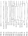
- the apparatus is indicated generally at 10 and includes a first circuit potion 12, a second circuit portion 14 and a switchover portion 16.
- a selecting (SEL) signal is applied on line 18 which is adapted to select either clock A (CLKA) or clock B (CLKB) depending upon the level of the SEL signal applied.
- CLKA clock A
- CLKB clock B
- Clock A is applied to the circuit portion 12 via line 20 which is adapted to clock each of three D-flip-flops 22, 24 and 26.
- the clock B signal is applied to the circuit potion 14 via lines 28 which also clock three D-flip-flops 30, 32 and 34.
- the output of flip-flop 22 provides a SEL_SYNCA signal on line 36 that is applied to an AND gate 38, the other input of which is SELB_SYNCA which is applied on line 40.
- the output of the AND gate 38 is applied via line 42 to the flip-flop 26 and its output provides the SELA signal on line 44 which is a handshake signal that extends to the input of flip-flop 30 in circuit portion 14.
- the AND gate 38 and other AND gates shown in FIG. 1 it should be understood that a small circle is shown on some of the inputs as well as on the output. This is intended to indicate that the logic level for that input or output is a active low or inverted level.
- Circuit portion 14 has a SELA_SYNCB signal on flip-flop 30 output line 46 and this signal is input to AND gate 48, the other input of which is SEL_SYNCB on line 50.
- the output of gate 48 on line 52 is input to the flip-flop 34, the output of which is the SELB handshake signal on line 54 that extends to the input of flip-flop 24.
- Lines 44 and 54 additionally are respectively applied to the switchover portion 16 and particularly to inputs of AND gates 56 and 58, the other inputs of which are clock A on line 20 and clock B on line 28.
- the output of the gates 56 and 58 are applied to the inputs of AND gate 60, the output of which is the clock out (CLKOUT) signal on line 62.
- a change in the SEL signal level from low to high switches the input clock signal that is to be used for generating the synchronized output signal from clock A to clock B.
- This high level is applied to both flip-flops 22 and 32, with the flip-flop 32 being clocked by the clock B signal whereas the flip-flop 22 is clocked by the clock A signal.
- the SEL signal is thereby synchronized to the clock A in circuit portion 12 and to clock B in circuit portion 14.
- the SEL signal is synchronized to clock A and that signal on line 36 results in the SELA signal going low as shown in FIG. 2 l which disables the switchover portion 16 causing the output clock CLKOUT signal on line 62 to be forced low as shown in FIG. 2g.
- the SEL signal is also synchronized to clock B by flip-flop 32 and the disabling of the clock A is propagated through the handshake signal via line 44 and flip-flop 30 and select SELB on line 54 is then switched high which enables clock B on the negative edge thereof as shown in FIG. 2f which results in the normal pulse width CLKOUT signal being produced on line 62 as shown in FIG. 2g.
- a R/S flip-flop has a 0 output default and a S/R flip-slop has a 1 output default. It should also be understood that the circuit illustrated in FIG. 1 has a default clock A operation upon application of the RESET NL signal on line 64. If the default value is to be clock B, then the type of flip-flops would be reversed from that shown in FIG. 1, i.e., an R/S type should be changed to an S/R type and visa versa.
Landscapes
- Engineering & Computer Science (AREA)
- Theoretical Computer Science (AREA)
- Physics & Mathematics (AREA)
- General Engineering & Computer Science (AREA)
- General Physics & Mathematics (AREA)
- Manipulation Of Pulses (AREA)
- Information Transfer Systems (AREA)
Applications Claiming Priority (2)
| Application Number | Priority Date | Filing Date | Title |
|---|---|---|---|
| US107118 | 1998-06-30 | ||
| US09/107,118 US6275546B1 (en) | 1998-06-30 | 1998-06-30 | Glitchless clock switch circuit |
Publications (2)
| Publication Number | Publication Date |
|---|---|
| EP0969350A2 true EP0969350A2 (de) | 2000-01-05 |
| EP0969350A3 EP0969350A3 (de) | 2001-01-31 |
Family
ID=22314947
Family Applications (1)
| Application Number | Title | Priority Date | Filing Date |
|---|---|---|---|
| EP99303975A Withdrawn EP0969350A3 (de) | 1998-06-30 | 1999-05-21 | Schaltung zur Umschaltung von Taktsignalen |
Country Status (3)
| Country | Link |
|---|---|
| US (1) | US6275546B1 (de) |
| EP (1) | EP0969350A3 (de) |
| JP (1) | JP2000138568A (de) |
Cited By (11)
| Publication number | Priority date | Publication date | Assignee | Title |
|---|---|---|---|---|
| WO2001050603A1 (en) * | 1999-12-30 | 2001-07-12 | Koninklijke Philips Electronics, Nv | Method and apparatus for selecting a clock signal without producing a glitch |
| WO2001059550A2 (en) * | 2000-02-08 | 2001-08-16 | Infineon Technologies North America Corp. | A secure asynchronous clock multiplexer |
| EP1202151A2 (de) * | 2000-10-31 | 2002-05-02 | Seiko Epson Corporation | Datensteueranlage und elektronisches Gerät |
| EP1263139A2 (de) * | 2001-05-30 | 2002-12-04 | STMicroelectronics Limited | Störimpulsfreier Multiplexer |
| US6774681B2 (en) | 2001-05-30 | 2004-08-10 | Stmicroelectronics Limited | Switchable clock source |
| US6982573B2 (en) | 2001-05-30 | 2006-01-03 | Stmicroelectronics Limited | Switchable clock source |
| EP1731985A1 (de) * | 2005-06-06 | 2006-12-13 | STMicroelectronics S.r.l. | Anordnung und Verfahren zum Taktschalten in getakten elektronischen Einrichtungen |
| EP1865400A1 (de) * | 2006-06-09 | 2007-12-12 | ATMEL Germany GmbH | Verfahren zum Umschalten eines Systemtakts und Taktsynchronisierungsvorrichtung |
| CN103792989A (zh) * | 2012-10-26 | 2014-05-14 | 硅谷实验室公司 | 处理停止时钟的无障碍时钟切换 |
| CN105406984A (zh) * | 2015-10-22 | 2016-03-16 | 上海斐讯数据通信技术有限公司 | 一种实现主备倒换背板时钟的系统及方法 |
| EP3197054A4 (de) * | 2014-09-16 | 2017-10-04 | Sanechips Technology Co., Ltd. | Dynamisches taktumschaltungsverfahren und vorrichtung sowie computerlesbares medium |
Families Citing this family (21)
| Publication number | Priority date | Publication date | Assignee | Title |
|---|---|---|---|---|
| US6792500B1 (en) * | 1998-07-08 | 2004-09-14 | Broadcom Corporation | Apparatus and method for managing memory defects |
| US7039146B2 (en) * | 2001-01-16 | 2006-05-02 | Advanced Micro Devices, Inc. | Method and interface for glitch-free clock switching |
| US6885714B1 (en) * | 2001-05-24 | 2005-04-26 | Cypress Semiconductor Corp. | Independently roving range control |
| US6600345B1 (en) * | 2001-11-15 | 2003-07-29 | Analog Devices, Inc. | Glitch free clock select switch |
| KR100437833B1 (ko) * | 2001-12-28 | 2004-06-30 | 주식회사 하이닉스반도체 | 클럭신호 스위치 회로 |
| US7003683B2 (en) * | 2002-01-31 | 2006-02-21 | Stmicroelectronics. Inc. | Glitchless clock selection circuit |
| JP3542351B2 (ja) * | 2002-11-18 | 2004-07-14 | 沖電気工業株式会社 | クロック切り替え回路 |
| US6873183B1 (en) | 2003-05-12 | 2005-03-29 | Xilinx, Inc. | Method and circuit for glitchless clock control |
| US6975145B1 (en) | 2003-06-02 | 2005-12-13 | Xilinx, Inc. | Glitchless dynamic multiplexer with synchronous and asynchronous controls |
| KR20050099714A (ko) * | 2004-04-12 | 2005-10-17 | 삼성전자주식회사 | 고집적 저전력 글리치리스 클럭 선택회로 및 이를구비하는 디지털 프로세싱 시스템 |
| US7129765B2 (en) | 2004-04-30 | 2006-10-31 | Xilinx, Inc. | Differential clock tree in an integrated circuit |
| US8073042B1 (en) | 2005-04-13 | 2011-12-06 | Cypress Semiconductor Corporation | Recursive range controller |
| US20080012605A1 (en) * | 2006-07-12 | 2008-01-17 | Eastman Kodak Company | Glitch-free clock switcher |
| JP5162877B2 (ja) * | 2006-10-18 | 2013-03-13 | 日本電気株式会社 | クロック非同期切替装置およびノイズキャンセル回路ならびにノイズキャンセル方法およびプログラム |
| WO2008114446A1 (ja) * | 2007-03-20 | 2008-09-25 | Fujitsu Microelectronics Limited | クロック信号選択回路 |
| US7471120B2 (en) * | 2007-05-15 | 2008-12-30 | Broadcom Corporation | Clock switch for generation of multi-frequency clock signal |
| US7944241B1 (en) * | 2010-01-29 | 2011-05-17 | Stmicroelectronics Pvt. Ltd. | Circuit for glitchless switching between asynchronous clocks |
| US8896347B2 (en) * | 2013-03-29 | 2014-11-25 | Hamilton Sundstrand Corporation | Synchronous input signal capture system |
| JP5880603B2 (ja) * | 2014-03-19 | 2016-03-09 | 日本電気株式会社 | クロック発生装置、サーバシステムおよびクロック制御方法 |
| US20160037123A1 (en) * | 2014-07-31 | 2016-02-04 | At&T Intellectual Property I, Lp | System and method for input sensing for internet protocol encoders |
| CN111262558B (zh) * | 2020-02-25 | 2023-05-26 | 云知声智能科技股份有限公司 | 一种快速无毛刺时钟切换电路实现方法及系统 |
Citations (4)
| Publication number | Priority date | Publication date | Assignee | Title |
|---|---|---|---|---|
| US4853653A (en) * | 1988-04-25 | 1989-08-01 | Rockwell International Corporation | Multiple input clock selector |
| US5289050A (en) * | 1991-03-29 | 1994-02-22 | Victor Company Of Japan, Ltd. | Clock signal selection circuit |
| US5502409A (en) * | 1993-03-04 | 1996-03-26 | Advanced Micro Devices | Clock switcher circuit |
| US5726593A (en) * | 1992-10-27 | 1998-03-10 | Nokia Telecommunications Oy | Method and circuit for switching between a pair of asynchronous clock signals |
Family Cites Families (5)
| Publication number | Priority date | Publication date | Assignee | Title |
|---|---|---|---|---|
| US5638083A (en) * | 1993-07-07 | 1997-06-10 | Chips And Technologies, Inc. | System for allowing synchronous sleep mode operation within a computer |
| US5572718A (en) * | 1994-06-14 | 1996-11-05 | Intel Corporation | Mechanism for dynamically determining and distributing computer system clocks |
| US5790609A (en) * | 1996-11-04 | 1998-08-04 | Texas Instruments Incorporated | Apparatus for cleanly switching between various clock sources in a data processing system |
| US5903746A (en) * | 1996-11-04 | 1999-05-11 | Texas Instruments Incorporated | Apparatus and method for automatically sequencing clocks in a data processing system when entering or leaving a low power state |
| US6094727A (en) * | 1998-06-23 | 2000-07-25 | Micron Technology, Inc. | Method and apparatus for controlling the data rate of a clocking circuit |
-
1998
- 1998-06-30 US US09/107,118 patent/US6275546B1/en not_active Expired - Lifetime
-
1999
- 1999-05-21 EP EP99303975A patent/EP0969350A3/de not_active Withdrawn
- 1999-06-09 JP JP11161930A patent/JP2000138568A/ja active Pending
Patent Citations (4)
| Publication number | Priority date | Publication date | Assignee | Title |
|---|---|---|---|---|
| US4853653A (en) * | 1988-04-25 | 1989-08-01 | Rockwell International Corporation | Multiple input clock selector |
| US5289050A (en) * | 1991-03-29 | 1994-02-22 | Victor Company Of Japan, Ltd. | Clock signal selection circuit |
| US5726593A (en) * | 1992-10-27 | 1998-03-10 | Nokia Telecommunications Oy | Method and circuit for switching between a pair of asynchronous clock signals |
| US5502409A (en) * | 1993-03-04 | 1996-03-26 | Advanced Micro Devices | Clock switcher circuit |
Cited By (21)
| Publication number | Priority date | Publication date | Assignee | Title |
|---|---|---|---|---|
| US6323715B1 (en) | 1999-12-30 | 2001-11-27 | Koninklijke Philips Electronics N.V. (Kpeuv) | Method and apparatus for selecting a clock signal without producing a glitch |
| WO2001050603A1 (en) * | 1999-12-30 | 2001-07-12 | Koninklijke Philips Electronics, Nv | Method and apparatus for selecting a clock signal without producing a glitch |
| WO2001059550A2 (en) * | 2000-02-08 | 2001-08-16 | Infineon Technologies North America Corp. | A secure asynchronous clock multiplexer |
| WO2001059550A3 (en) * | 2000-02-08 | 2002-03-28 | Infineon Technologies Corp | A secure asynchronous clock multiplexer |
| US6535048B1 (en) | 2000-02-08 | 2003-03-18 | Infineon Technologies North America Corp. | Secure asynchronous clock multiplexer |
| US7047434B2 (en) | 2000-10-31 | 2006-05-16 | Seiko Epson Corporation | Data transfer control device and electronic equipment |
| EP1202151A2 (de) * | 2000-10-31 | 2002-05-02 | Seiko Epson Corporation | Datensteueranlage und elektronisches Gerät |
| EP1202151A3 (de) * | 2000-10-31 | 2003-05-21 | Seiko Epson Corporation | Datensteueranlage und elektronisches Gerät |
| EP1263139A2 (de) * | 2001-05-30 | 2002-12-04 | STMicroelectronics Limited | Störimpulsfreier Multiplexer |
| US6982573B2 (en) | 2001-05-30 | 2006-01-03 | Stmicroelectronics Limited | Switchable clock source |
| US6774681B2 (en) | 2001-05-30 | 2004-08-10 | Stmicroelectronics Limited | Switchable clock source |
| EP1263139A3 (de) * | 2001-05-30 | 2006-07-05 | STMicroelectronics Limited | Störimpulsfreier Multiplexer |
| EP1731985A1 (de) * | 2005-06-06 | 2006-12-13 | STMicroelectronics S.r.l. | Anordnung und Verfahren zum Taktschalten in getakten elektronischen Einrichtungen |
| EP1865400A1 (de) * | 2006-06-09 | 2007-12-12 | ATMEL Germany GmbH | Verfahren zum Umschalten eines Systemtakts und Taktsynchronisierungsvorrichtung |
| DE102006026914A1 (de) * | 2006-06-09 | 2007-12-20 | Atmel Germany Gmbh | Verfahren zum Umschalten eines Systemtakts und Taktsynchronisierungsvorrichtung |
| DE102006026914B4 (de) * | 2006-06-09 | 2008-02-28 | Atmel Germany Gmbh | Verfahren zum Umschalten eines Systemtakts und Taktsynchronisierungsvorrichtung |
| US7605617B2 (en) | 2006-06-09 | 2009-10-20 | Atmel Automotive Gmbh | Method for switching a system clock and clock synchronization unit |
| CN103792989A (zh) * | 2012-10-26 | 2014-05-14 | 硅谷实验室公司 | 处理停止时钟的无障碍时钟切换 |
| CN103792989B (zh) * | 2012-10-26 | 2019-02-15 | 硅谷实验室公司 | 处理停止时钟的无障碍时钟切换 |
| EP3197054A4 (de) * | 2014-09-16 | 2017-10-04 | Sanechips Technology Co., Ltd. | Dynamisches taktumschaltungsverfahren und vorrichtung sowie computerlesbares medium |
| CN105406984A (zh) * | 2015-10-22 | 2016-03-16 | 上海斐讯数据通信技术有限公司 | 一种实现主备倒换背板时钟的系统及方法 |
Also Published As
| Publication number | Publication date |
|---|---|
| US6275546B1 (en) | 2001-08-14 |
| EP0969350A3 (de) | 2001-01-31 |
| JP2000138568A (ja) | 2000-05-16 |
Similar Documents
| Publication | Publication Date | Title |
|---|---|---|
| US6275546B1 (en) | Glitchless clock switch circuit | |
| US5315181A (en) | Circuit for synchronous, glitch-free clock switching | |
| US6600345B1 (en) | Glitch free clock select switch | |
| US5764710A (en) | Meta-stable-resistant front-end to a synchronizer with asynchronous clear and asynchronous second-stage clock selector | |
| US6359479B1 (en) | Synchronizing data transfers between two distinct clock domains | |
| US4855616A (en) | Apparatus for synchronously switching frequency source | |
| US20080054952A1 (en) | Circuit for switching between two clock signals independently of the frequency of the clock signals | |
| US5313470A (en) | Boundary-scan input cell for a clock pin | |
| US6049236A (en) | Divide-by-one or divide-by-two qualified clock driver with glitch-free transitions between operating frequencies | |
| US6535048B1 (en) | Secure asynchronous clock multiplexer | |
| US5926044A (en) | Clock switching device and method | |
| KR20080101495A (ko) | 클럭 스위칭 회로 | |
| GB2365234A (en) | Selective modification of a clock pulse train | |
| US4823365A (en) | Synchronization method and elastic buffer circuit | |
| EP1096683A1 (de) | Taktgeberschaltung | |
| US6882184B2 (en) | Clock switching circuit | |
| US6075398A (en) | Tunable digital oscillator circuit and method for producing clock signals of different frequencies | |
| US6040723A (en) | Interface circuit with high speed data transmission | |
| JPH0771055B2 (ja) | 高速度信号多重化装置 | |
| US7555083B2 (en) | Synchronizing circuit for stably generating an output signal | |
| JP3562321B2 (ja) | クロック信号切り換え装置 | |
| KR19980050372A (ko) | 데이타 전송 동기용 클럭 발생장치 | |
| JPS62202624A (ja) | 高速デ−タ受信回路方式 | |
| EP1263139A2 (de) | Störimpulsfreier Multiplexer | |
| CN117411465A (zh) | 一种时钟切换电路、芯片及电子设备 |
Legal Events
| Date | Code | Title | Description |
|---|---|---|---|
| PUAI | Public reference made under article 153(3) epc to a published international application that has entered the european phase |
Free format text: ORIGINAL CODE: 0009012 |
|
| AK | Designated contracting states |
Kind code of ref document: A2 Designated state(s): DE FR GB |
|
| AX | Request for extension of the european patent |
Free format text: AL;LT;LV;MK;RO;SI |
|
| PUAL | Search report despatched |
Free format text: ORIGINAL CODE: 0009013 |
|
| AK | Designated contracting states |
Kind code of ref document: A3 Designated state(s): AT BE CH CY DE DK ES FI FR GB GR IE IT LI LU MC NL PT SE |
|
| AX | Request for extension of the european patent |
Free format text: AL;LT;LV;MK;RO;SI |
|
| RIC1 | Information provided on ipc code assigned before grant |
Free format text: 7G 06F 1/12 A, 7G 06F 1/08 B |
|
| RAP1 | Party data changed (applicant data changed or rights of an application transferred) |
Owner name: HEWLETT-PACKARD COMPANY, A DELAWARE CORPORATION |
|
| 17P | Request for examination filed |
Effective date: 20010611 |
|
| AKX | Designation fees paid |
Free format text: DE FR GB |
|
| 17Q | First examination report despatched |
Effective date: 20060119 |
|
| GRAP | Despatch of communication of intention to grant a patent |
Free format text: ORIGINAL CODE: EPIDOSNIGR1 |
|
| STAA | Information on the status of an ep patent application or granted ep patent |
Free format text: STATUS: THE APPLICATION IS DEEMED TO BE WITHDRAWN |
|
| 18D | Application deemed to be withdrawn |
Effective date: 20080528 |