EP0959650A1 - Umgossene elektronische Baugruppe - Google Patents
Umgossene elektronische Baugruppe Download PDFInfo
- Publication number
- EP0959650A1 EP0959650A1 EP99201074A EP99201074A EP0959650A1 EP 0959650 A1 EP0959650 A1 EP 0959650A1 EP 99201074 A EP99201074 A EP 99201074A EP 99201074 A EP99201074 A EP 99201074A EP 0959650 A1 EP0959650 A1 EP 0959650A1
- Authority
- EP
- European Patent Office
- Prior art keywords
- circuit board
- heat
- conductive member
- recited
- assembly
- Prior art date
- Legal status (The legal status is an assumption and is not a legal conclusion. Google has not performed a legal analysis and makes no representation as to the accuracy of the status listed.)
- Withdrawn
Links
- 238000000034 method Methods 0.000 claims abstract description 21
- 239000000463 material Substances 0.000 claims abstract description 13
- 238000000465 moulding Methods 0.000 claims abstract description 9
- 238000004519 manufacturing process Methods 0.000 abstract description 3
- 230000000712 assembly Effects 0.000 description 3
- 238000000429 assembly Methods 0.000 description 3
- 239000002184 metal Substances 0.000 description 3
- 239000004020 conductor Substances 0.000 description 2
- 239000003989 dielectric material Substances 0.000 description 2
- 238000011065 in-situ storage Methods 0.000 description 1
- 230000001681 protective effect Effects 0.000 description 1
- 238000007789 sealing Methods 0.000 description 1
- 239000004065 semiconductor Substances 0.000 description 1
- 230000035939 shock Effects 0.000 description 1
Images

Classifications
-
- H—ELECTRICITY
- H05—ELECTRIC TECHNIQUES NOT OTHERWISE PROVIDED FOR
- H05K—PRINTED CIRCUITS; CASINGS OR CONSTRUCTIONAL DETAILS OF ELECTRIC APPARATUS; MANUFACTURE OF ASSEMBLAGES OF ELECTRICAL COMPONENTS
- H05K5/00—Casings, cabinets or drawers for electric apparatus
- H05K5/0026—Casings, cabinets or drawers for electric apparatus provided with connectors and printed circuit boards [PCB], e.g. automotive electronic control units
- H05K5/0034—Casings, cabinets or drawers for electric apparatus provided with connectors and printed circuit boards [PCB], e.g. automotive electronic control units having an overmolded housing covering the PCB
-
- H—ELECTRICITY
- H05—ELECTRIC TECHNIQUES NOT OTHERWISE PROVIDED FOR
- H05K—PRINTED CIRCUITS; CASINGS OR CONSTRUCTIONAL DETAILS OF ELECTRIC APPARATUS; MANUFACTURE OF ASSEMBLAGES OF ELECTRICAL COMPONENTS
- H05K3/00—Apparatus or processes for manufacturing printed circuits
- H05K3/0058—Laminating printed circuit boards onto other substrates, e.g. metallic substrates
- H05K3/0061—Laminating printed circuit boards onto other substrates, e.g. metallic substrates onto a metallic substrate, e.g. a heat sink
-
- H—ELECTRICITY
- H05—ELECTRIC TECHNIQUES NOT OTHERWISE PROVIDED FOR
- H05K—PRINTED CIRCUITS; CASINGS OR CONSTRUCTIONAL DETAILS OF ELECTRIC APPARATUS; MANUFACTURE OF ASSEMBLAGES OF ELECTRICAL COMPONENTS
- H05K3/00—Apparatus or processes for manufacturing printed circuits
- H05K3/22—Secondary treatment of printed circuits
- H05K3/28—Applying non-metallic protective coatings
- H05K3/284—Applying non-metallic protective coatings for encapsulating mounted components
-
- H—ELECTRICITY
- H05—ELECTRIC TECHNIQUES NOT OTHERWISE PROVIDED FOR
- H05K—PRINTED CIRCUITS; CASINGS OR CONSTRUCTIONAL DETAILS OF ELECTRIC APPARATUS; MANUFACTURE OF ASSEMBLAGES OF ELECTRICAL COMPONENTS
- H05K7/00—Constructional details common to different types of electric apparatus
- H05K7/20—Modifications to facilitate cooling, ventilating, or heating
- H05K7/20845—Modifications to facilitate cooling, ventilating, or heating for automotive electronic casings
- H05K7/20854—Heat transfer by conduction from internal heat source to heat radiating structure
-
- H—ELECTRICITY
- H05—ELECTRIC TECHNIQUES NOT OTHERWISE PROVIDED FOR
- H05K—PRINTED CIRCUITS; CASINGS OR CONSTRUCTIONAL DETAILS OF ELECTRIC APPARATUS; MANUFACTURE OF ASSEMBLAGES OF ELECTRICAL COMPONENTS
- H05K2201/00—Indexing scheme relating to printed circuits covered by H05K1/00
- H05K2201/09—Shape and layout
- H05K2201/09209—Shape and layout details of conductors
- H05K2201/09654—Shape and layout details of conductors covering at least two types of conductors provided for in H05K2201/09218 - H05K2201/095
- H05K2201/09754—Connector integrally incorporated in the printed circuit board [PCB] or in housing
-
- H—ELECTRICITY
- H05—ELECTRIC TECHNIQUES NOT OTHERWISE PROVIDED FOR
- H05K—PRINTED CIRCUITS; CASINGS OR CONSTRUCTIONAL DETAILS OF ELECTRIC APPARATUS; MANUFACTURE OF ASSEMBLAGES OF ELECTRICAL COMPONENTS
- H05K2203/00—Indexing scheme relating to apparatus or processes for manufacturing printed circuits covered by H05K3/00
- H05K2203/13—Moulding and encapsulation; Deposition techniques; Protective layers
- H05K2203/1305—Moulding and encapsulation
- H05K2203/1327—Moulding over PCB locally or completely
Definitions
- the present invention generally relates to electronic assemblies. More particularly, this invention relates to an overmolded electronic assembly that is compatible with automated assembly methods and yields an enclosure of the type that conducts heat away from a flip chip or other circuit device enclosed within the assembly.
- Circuit boards with semiconductor devices such as flip chips must often be protected from the environment in which the board is employed.
- a widely practiced method is to enclose such circuit boards in an assembly that includes a pair of case halves that must be assembled together by hand to form an enclosure that supports the circuit board within. Connectors secured to one of the case halves provide for electrical interconnection to the circuit board. Sealing elements are also typically required to exclude moisture from the enclosure. Finally, fasteners are required to secure the assembly together.
- Such assembly processes are labor intensive, and the resulting package must be tested for leakage to ensure the package was properly assembled.
- an overmolded electronic assembly and a method for forming the assembly that entails enclosing a circuit board having one or more circuit devices mounted to its surface.
- the assembly includes a heat-conductive member in thermal contact with one or more of the circuit devices mounted to the circuit board.
- An overmolded body encloses the circuit board and the circuit device with the heat-conductive member, such that the overmolded body and heat-conductive member form a moisture-impermeable seal around the circuit board and circuit device.
- the overmolded body also has a connector housing integrally-formed in its outer surface.
- the method for manufacturing the overmolded electronic assembly generally entails supporting the circuit board on the heat-conductive member such that the heat-conductive member thermally contacts the circuit device.
- An overmolded enclosure is then formed by molding a material over the surface of the circuit board to form the overmolded body that, with the heat-conductive member, encloses the circuit board and its circuit device.
- the heat-conductive member includes pedestals that contact the circuit devices, supports space the circuit board from the heat-conductive member, and the circuit board has input/output pins that extend through the overmolded body and into the connector housing.
- the circuit board, supports and heat-conductive member define a cavity into which the material for the overmolded enclosure flows during molding to encase the circuit board.
- the assembly further includes a snap-fit member that is mechanically locked to the heat-conductive member, with the circuit board being enclosed between the snap-fit member and the heat-conductive member.
- the snap-fit member preferably biases the circuit device against the heat-conductive member, and provides EMI shielding for the circuit board.
- the overmolded body is formed by molding a material over the exterior surface of the snap-fit member, such that the overmolded body and heat-conductive member enclose and encase the circuit board and snap-fit member.
- the overmolded electronic assembly of this invention provides an uncomplicated method for encasing a circuit board and its circuit devices in a protective enclosure. More particularly, the assembly eliminates the prior art requirement for separate connectors, individual case assemblies, fasteners and seals. In the manufacturing process, there is no assembly of seals to case halves, no fastening of case halves, reduced inventory of parts and no leak test requirement. Furthermore, the electronic assembly can be manufactured on a completely automated final assembly line. Finally, the electronic assembly can exhibit improved heat transfer from the circuit devices, resistance to vibration and shock, and improved reliability due to more closely matched coefficients of thermal expansion (CTE) of the overmolding and circuit board materials.
- CTE coefficients of thermal expansion
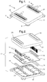
- FIGs 1, 2 and 4 show an overmolded electronic assembly 10 enclosing a circuit board 12 in accordance with a first embodiment of this invention.
- the circuit board 12 may be a thin laminate, printed wiring board (PWB), or any other material known in the an. Shown mounted to one surface of the circuit board 12 in Figure 4 are several IC packages 16 that dissipate heat. The packages 16 will typically be flip chips, though the invention is applicable to essentially any surface-mount device.
- the circuit board 12 includes I/O (input/output) connector pins 14 electrically interconnected with the IC packages 16 in any suitable manner.
- the assembly 10 includes a heatsink 18 formed of a thermally conductive material, such as a metal or a metal-filled plastic.
- the heatsink 18 has a number of pedestals 20 in thermal contact with the IC packages 16, such that heat is conducted from the packages 16 and into the heatsink 18 for subsequent dissipation to the surrounding environment.
- An overmolded housing 22 encases the circuit board 12, contacting the upper surface of the circuit board 12 (opposite the IC packages 16) and underfilling the circuit board 12, and therefore contacting the heatsink 18 and the lower surface of the board 12. In this manner, the overmolded housing 22 forms a moisture-impermeable seal around the circuit board 12 and its IC packages 16, as best seen in Figure 4.
- the overmolded housing 22 includes a pair of integrally-formed connector housings 28 into which the pins 14 project, such that the pins 14 and connector housings 28 form a pair of connectors on the exterior of the electronic assembly 10.
- the circuit board 12 is preferably preassembled with the pins 14 and dielectric pin retainers 26, with a pair of the retainers 26 being positioned on each side of the circuit board 12.
- the pins 14 extend through the retainers 26 on the upper surface of the circuit board 12, through the circuit board 12, and into the retainers 26 on the lower surface of the circuit board 12, such that the pins 14 project above the surface of the upper pair of retainers 26 as shown.
- the circuit board 12 is then placed on the heatsink 18 such that the heatsink 18, and particularly the pedestals 20, thermally contact the IC packages 16.
- the lower pin retainers 26 support and space the circuit board 12 above the heatsink 18.
- the overmolded housing 22 is then molded in-situ by molding a suitable dielectric material over the subassembly formed by the circuit board 12 and heatsink 18.
- the material for the housing 22 flows over, around and under the circuit board 12 to encase the board 12.
- the heatsink 18, pin retainers 26 and circuit board 12 are insert-molded within the tooling in which the housing 22 is formed.
- the upper pin retainers 26 support the tooling during molding of the housing 22.
- the tooling is appropriately configured to integrally form the connector housings 28 in the appropriate location on the overmolded housing 22, forming electrical connectors with the pins 14 that protrude through the housing 22.
- Suitable materials for the housing 22 include those used to form the IC packages, though it is foreseeable that other moldable dielectric materials could be used.
- an electronic assembly 110 is formed similarly to the assembly 10 of Figures 1, 2 and 4, but further includes a snap-fit retainer 130 that is also insert-molded during overmolding of a housing 122. Similar to the first embodiment, the assembly 110 includes a circuit board 12 with connector pins 14, IC packages (not shown) and pin retainers 126, a heatsink 118 with pedestals 120, and the overmolded housing 122.
- the retainer 130 is preferably formed from a metal or other electrically-conductive material, such that the retainer 130 provides EMI shielding of the IC packages.
- the retainer 130 includes integrally-formed locking appendages 132 that interlock with the heatsink 118, and biasing members 134 that apply pressure to the near surface of the circuit board 112 to promote thermal contact between the IC packages and the pedestals 120 on the heatsink 118.
- the locking appendages 132 and biasing members 134 can be any suitable elements, such as the resilient cantilevered springs shown in Figure 3. Locking appendages 132 and biasing members 134 of this type can be readily formed when the retainer 130 is fabricated by stamping. However, it is foreseeable that other elements could be used for these purposes, such as elastomeric pads located on the lower surface of the retainer 130 to contact the circuit board 112.
- the process for assembling the electronic assembly 110 of Figure 3 is similar to that for the assembly 10 of Figures 1, 2 and 4, but with the retainer 130 being mounted to the subassembly formed by the circuit board 12 and heatsink 118 prior to overmolding the housing 122. In this manner, the circuit board 112 is enclosed between the retainer 130 and the heatsink 118. The material for the overmolded housing 122 is then molded directly over the retainer 130, such that the housing 122 directly contacts and covers the retainer 130, as well as the dielectric pin retainers 126, the circuit board 12 and the heatsink 118.
Landscapes
- Engineering & Computer Science (AREA)
- Microelectronics & Electronic Packaging (AREA)
- Manufacturing & Machinery (AREA)
- Physics & Mathematics (AREA)
- Thermal Sciences (AREA)
- Shielding Devices Or Components To Electric Or Magnetic Fields (AREA)
Applications Claiming Priority (2)
| Application Number | Priority Date | Filing Date | Title |
|---|---|---|---|
| US81498 | 1998-05-20 | ||
| US09/081,498 US6180045B1 (en) | 1998-05-20 | 1998-05-20 | Method of forming an overmolded electronic assembly |
Publications (1)
| Publication Number | Publication Date |
|---|---|
| EP0959650A1 true EP0959650A1 (de) | 1999-11-24 |
Family
ID=22164574
Family Applications (1)
| Application Number | Title | Priority Date | Filing Date |
|---|---|---|---|
| EP99201074A Withdrawn EP0959650A1 (de) | 1998-05-20 | 1999-04-06 | Umgossene elektronische Baugruppe |
Country Status (2)
| Country | Link |
|---|---|
| US (2) | US6180045B1 (de) |
| EP (1) | EP0959650A1 (de) |
Cited By (4)
| Publication number | Priority date | Publication date | Assignee | Title |
|---|---|---|---|---|
| WO2009013653A1 (en) * | 2007-07-23 | 2009-01-29 | Ford Otomotiv Sanayi Anonim Sirketi | A bottom mounting part |
| EP1740027A3 (de) * | 2005-06-27 | 2009-06-03 | Delphi Technologies, Inc. | Hertellungsverfahren einer umgossenen elektronischen Baugruppe |
| EP1686844A3 (de) * | 2005-01-28 | 2010-03-03 | Delphi Technologies, Inc. | Umgossene elektronische Baugruppe mit einsatzgeformten Wärmesenken |
| EP2807907B1 (de) | 2012-01-26 | 2015-11-04 | WABCO GmbH | Verfahren zum herstellen eines steuergerätgehäuses sowie ein nach diesem verfahren hergestelltes steuergerätgehäuse |
Families Citing this family (55)
| Publication number | Priority date | Publication date | Assignee | Title |
|---|---|---|---|---|
| TW451535B (en) | 1998-09-04 | 2001-08-21 | Sony Corp | Semiconductor device and package, and fabrication method thereof |
| JP2000326359A (ja) * | 1999-05-20 | 2000-11-28 | Hitachi Ltd | プリモールド部材を用いた複合一体成形品 |
| JP3270028B2 (ja) * | 1999-09-10 | 2002-04-02 | 株式会社ソニー・コンピュータエンタテインメント | 電磁シールド板、電磁シールド構造体及びエンタテインメント装置 |
| US6349036B1 (en) * | 2000-05-29 | 2002-02-19 | Jess-Link Products Co., Ltd. | Adaptive seat of computer functional cards |
| US6617195B1 (en) * | 2000-07-24 | 2003-09-09 | Advanced Micro Devices, Inc. | Method of reflowing organic packages using no-clean flux |
| US6307749B1 (en) | 2000-10-23 | 2001-10-23 | Delphi Technologies, Inc. | Overmolded electronic module with underfilled surface-mount components |
| US6560110B1 (en) * | 2002-02-22 | 2003-05-06 | Delphi Technologies, Inc. | Corrosive resistant flip chip thermal management structure |
| US6807731B2 (en) * | 2002-04-02 | 2004-10-26 | Delphi Technologies, Inc. | Method for forming an electronic assembly |
| US20040132322A1 (en) * | 2003-01-07 | 2004-07-08 | Brandenburg Scott D. | Filtered electrical connector assembly for an overmolded electronic package |
| US6873043B2 (en) * | 2003-03-10 | 2005-03-29 | Delphi Technologies, Inc. | Electronic assembly having electrically-isolated heat-conductive structure |
| US6700195B1 (en) | 2003-03-26 | 2004-03-02 | Delphi Technologies, Inc. | Electronic assembly for removing heat from a flip chip |
| US6779260B1 (en) | 2003-03-28 | 2004-08-24 | Delphi Technologies, Inc. | Overmolded electronic package including circuit-carrying substrate |
| US7134194B2 (en) * | 2003-11-13 | 2006-11-14 | Delphi Technologies, Inc. | Method of developing an electronic module |
| US6905349B1 (en) * | 2004-02-23 | 2005-06-14 | Delphi Technologies, Inc. | Technique for connector to printed circuit board decoupling to eliminate flexure |
| JP2006032490A (ja) * | 2004-07-13 | 2006-02-02 | Hitachi Ltd | エンジン制御回路装置 |
| US7553680B2 (en) * | 2004-08-09 | 2009-06-30 | Delphi Technologies, Inc. | Methods to provide and expose a diagnostic connector on overmolded electronic packages |
| JP4478007B2 (ja) * | 2004-12-16 | 2010-06-09 | 日立オートモティブシステムズ株式会社 | 電子回路装置及びその製造方法 |
| US7473585B2 (en) * | 2005-06-13 | 2009-01-06 | Delphi Technologies, Inc. | Technique for manufacturing an overmolded electronic assembly |
| US7189335B1 (en) * | 2005-08-31 | 2007-03-13 | Honeywell International Inc. | Conformal coverings for electronic devices |
| US7209360B1 (en) * | 2005-10-28 | 2007-04-24 | Lear Corporation | Leak-tight system for boxes containing electrical and electronic components |
| US7403385B2 (en) * | 2006-03-06 | 2008-07-22 | Cisco Technology, Inc. | Efficient airflow management |
| US7616448B2 (en) * | 2007-09-14 | 2009-11-10 | Delphi Technologies, Inc. | Wrap-around overmold for electronic assembly |
| US7603770B2 (en) * | 2007-09-28 | 2009-10-20 | Delphi Technologies, Inc. | Method of overmolding an electronic assembly having an insert-molded vertical mount connector header |
| US20090091889A1 (en) * | 2007-10-09 | 2009-04-09 | Oman Todd P | Power electronic module having improved heat dissipation capability |
| US7739791B2 (en) | 2007-10-26 | 2010-06-22 | Delphi Technologies, Inc. | Method of producing an overmolded electronic module with a flexible circuit pigtail |
| WO2009069542A1 (ja) * | 2007-11-29 | 2009-06-04 | Ngk Spark Plug Co., Ltd. | 金属樹脂複合体 |
| US20090268414A1 (en) * | 2008-04-23 | 2009-10-29 | Bo Lu | Over-molded electronic module |
| US8081466B2 (en) * | 2009-07-06 | 2011-12-20 | Rockwell Automation Technologies, Inc. | Overmolded electronics enclosure |
| JP2011100718A (ja) * | 2009-10-05 | 2011-05-19 | Yazaki Corp | コネクタ |
| US7909657B1 (en) | 2009-11-12 | 2011-03-22 | Hubbell Incorporated | Electrical connector with low-stress, reduced-electrical-length contacts |
| DE102010002947A1 (de) * | 2010-03-17 | 2011-09-22 | Robert Bosch Gmbh | Steuergerät |
| US8555493B2 (en) * | 2010-04-23 | 2013-10-15 | Psion, Inc. | Method of manufacturing a molded printed circuit board |
| US8817483B2 (en) * | 2011-08-01 | 2014-08-26 | Honeywell International Inc. | Connector assembly for a sensor |
| DE102011113929B4 (de) * | 2011-09-21 | 2016-11-24 | Oechsler Aktiengesellschaft | Elektromechanischer Schaltungsaufbau |
| DE102012207877A1 (de) * | 2012-05-11 | 2013-11-14 | Robert Bosch Gmbh | Baugruppe für eine vorkonfektionierte Anschlussleiste sowie Verfahren zum Herstellen vorkonfektionierter Anschlussleisten |
| EP2873125A1 (de) * | 2012-07-12 | 2015-05-20 | Labinal, LLC | Lastschienenanordnung und verfahren zu ihrer herstellung |
| WO2014113323A1 (en) | 2013-01-15 | 2014-07-24 | Basf Se | A method of encapsulating an electronic component |
| US8898897B2 (en) | 2013-02-12 | 2014-12-02 | Joseph Lai | Method of making user-friendly USB male connector |
| KR101449271B1 (ko) * | 2013-04-19 | 2014-10-08 | 현대오트론 주식회사 | 오버몰딩을 이용한 차량의 전자 제어 장치 및 그 제조 방법 |
| KR101428933B1 (ko) * | 2013-07-05 | 2014-08-08 | 현대오트론 주식회사 | 방열판을 이용한 차량의 전자 제어 장치 및 그 제조 방법 |
| US9622355B2 (en) * | 2013-07-08 | 2017-04-11 | Delphi Technologies, Inc. | Environmentally sealed electrical housing assembly with integrated connector |
| US20150016077A1 (en) * | 2013-07-15 | 2015-01-15 | Delphi Technologies, Inc. | Electrical center for a vehicle |
| DE102013215367A1 (de) * | 2013-08-05 | 2015-02-05 | Zf Friedrichshafen Ag | Elektronisches Schaltungsmodul |
| US9579511B2 (en) | 2014-12-15 | 2017-02-28 | Medtronic, Inc. | Medical device with surface mounted lead connector |
| US9293870B1 (en) * | 2015-03-10 | 2016-03-22 | Continental Automotive Systems, Inc. | Electronic control module having a cover allowing for inspection of right angle press-fit pins |
| DE102015207867A1 (de) * | 2015-04-29 | 2016-11-03 | Robert Bosch Gmbh | Elektronische Baugruppe, insbesondere für ein Getriebesteuermodul |
| US9781819B2 (en) * | 2015-07-31 | 2017-10-03 | Laird Technologies, Inc. | Multifunctional components for electronic devices and related methods of providing thermal management and board level shielding |
| US10881014B2 (en) | 2015-09-29 | 2020-12-29 | Hitachi Automotive Systems, Ltd. | Electronic control device, and manufacturing method for vehicle-mounted electronic control device |
| US10517181B2 (en) | 2015-09-29 | 2019-12-24 | Hitachi Automotive Systems, Ltd. | Electronic control device and manufacturing method for same |
| WO2017056727A1 (ja) * | 2015-09-29 | 2017-04-06 | 日立オートモティブシステムズ株式会社 | 電子制御装置 |
| US20170356640A1 (en) | 2016-06-10 | 2017-12-14 | Innotec, Corp. | Illumination assembly including thermal energy management |
| CN108934132B (zh) * | 2017-05-25 | 2021-08-06 | 法雷奥汽车内部控制(深圳)有限公司 | 印刷电路板组件及其封装方法和机动车辆 |
| DE102019200768A1 (de) * | 2019-01-23 | 2020-07-23 | Zf Friedrichshafen Ag | Verfahren und Werkzeug zum Umspritzen eines Elektronikmoduls und umspritztes Elektronikmodul |
| DE102019113068A1 (de) * | 2019-05-17 | 2020-11-19 | Marelli Automotive Lighting Reutlingen (Germany) GmbH | Leiterplatte mit einer Steckverbindung |
| EP4292170A4 (de) * | 2021-02-12 | 2024-11-13 | Ideal Industries Inc. | Systeme und verfahren für gehäuse eines elektrischen verbinders und eingeschlossene leiterplatte |
Citations (2)
| Publication number | Priority date | Publication date | Assignee | Title |
|---|---|---|---|---|
| US4843520A (en) * | 1987-02-03 | 1989-06-27 | Matsushita Electric Industrial Co. Ltd. | Electronic circuit module |
| EP0641154A1 (de) * | 1993-08-30 | 1995-03-01 | TEMIC TELEFUNKEN microelectronic GmbH | Baugruppe zur Aufnahme elektronischer Bauelemente |
Family Cites Families (7)
| Publication number | Priority date | Publication date | Assignee | Title |
|---|---|---|---|---|
| EP0268181B1 (de) * | 1986-11-15 | 1992-07-29 | Matsushita Electric Works, Ltd. | Gegossenes Kunststoff-Chip-Gehäuse mit Steckermuster |
| US5420752A (en) * | 1993-08-18 | 1995-05-30 | Lsi Logic Corporation | GPT system for encapsulating an integrated circuit package |
| US5444909A (en) * | 1993-12-29 | 1995-08-29 | Intel Corporation | Method of making a drop-in heat sink |
| US5701034A (en) * | 1994-05-03 | 1997-12-23 | Amkor Electronics, Inc. | Packaged semiconductor die including heat sink with locking feature |
| US5625226A (en) * | 1994-09-19 | 1997-04-29 | International Rectifier Corporation | Surface mount package with improved heat transfer |
| EP0817261B1 (de) * | 1996-06-28 | 2003-04-23 | STMicroelectronics S.r.l. | Verfahren zur Herstellung einer Plastikpackung für eine elektronische Anordnung mit vollständig isolierter Wärmesenke |
| US5774342A (en) * | 1996-09-26 | 1998-06-30 | Delco Electronics Corporation | Electronic circuit with integrated terminal pins |
-
1998
- 1998-05-20 US US09/081,498 patent/US6180045B1/en not_active Expired - Lifetime
-
1999
- 1999-04-06 EP EP99201074A patent/EP0959650A1/de not_active Withdrawn
-
2000
- 2000-10-20 US US09/692,241 patent/US6285551B1/en not_active Expired - Lifetime
Patent Citations (2)
| Publication number | Priority date | Publication date | Assignee | Title |
|---|---|---|---|---|
| US4843520A (en) * | 1987-02-03 | 1989-06-27 | Matsushita Electric Industrial Co. Ltd. | Electronic circuit module |
| EP0641154A1 (de) * | 1993-08-30 | 1995-03-01 | TEMIC TELEFUNKEN microelectronic GmbH | Baugruppe zur Aufnahme elektronischer Bauelemente |
Cited By (4)
| Publication number | Priority date | Publication date | Assignee | Title |
|---|---|---|---|---|
| EP1686844A3 (de) * | 2005-01-28 | 2010-03-03 | Delphi Technologies, Inc. | Umgossene elektronische Baugruppe mit einsatzgeformten Wärmesenken |
| EP1740027A3 (de) * | 2005-06-27 | 2009-06-03 | Delphi Technologies, Inc. | Hertellungsverfahren einer umgossenen elektronischen Baugruppe |
| WO2009013653A1 (en) * | 2007-07-23 | 2009-01-29 | Ford Otomotiv Sanayi Anonim Sirketi | A bottom mounting part |
| EP2807907B1 (de) | 2012-01-26 | 2015-11-04 | WABCO GmbH | Verfahren zum herstellen eines steuergerätgehäuses sowie ein nach diesem verfahren hergestelltes steuergerätgehäuse |
Also Published As
| Publication number | Publication date |
|---|---|
| US6180045B1 (en) | 2001-01-30 |
| US6285551B1 (en) | 2001-09-04 |
Similar Documents
| Publication | Publication Date | Title |
|---|---|---|
| US6285551B1 (en) | Overmolded electronic assembly | |
| US6307749B1 (en) | Overmolded electronic module with underfilled surface-mount components | |
| US5930115A (en) | Apparatus, method and system for thermal management of a semiconductor device | |
| US6580167B1 (en) | Heat spreader with spring IC package | |
| EP1646271B1 (de) | Steuervorrichtung und Verfahren zu deren Herstellung | |
| US6445592B1 (en) | Electronic assembly | |
| EP0723737B1 (de) | Periphere computerkarte mit einem festen einteiligen gehaeuse und deren herstellungsverfahren | |
| US5677511A (en) | Overmolded PC board with ESD protection and EMI suppression | |
| US4766520A (en) | Injection molded circuit housing | |
| US20050081377A1 (en) | Method for forming an electronic assembly | |
| US20040109292A1 (en) | Reversible heat sink packaging assembly for an integrated circuit | |
| US5737187A (en) | Apparatus, method and system for thermal management of an unpackaged semiconductor device | |
| EP2053907A2 (de) | Verfahren zur Herstellung eines umgegossenen elektronischen Moduls mit flexibler Schaltkreisanschlusslitze | |
| US6562655B1 (en) | Heat spreader with spring IC package fabrication method | |
| CN109005317B (zh) | 用于摄像机的壳体及制造方法 | |
| KR100759724B1 (ko) | 제거가능한 커넥터를 위한 전자 제어 모듈 및 그 조립 방법 | |
| US6392887B1 (en) | PLGA-BGA socket using elastomer connectors | |
| US20080036057A1 (en) | Semiconductor device having improved heat dissipation capabilities | |
| US5959840A (en) | Apparatus for cooling multiple printed circuit board mounted electrical components | |
| WO2003023852A1 (en) | Semiconductor package | |
| CN110603693B (zh) | 电子模块和制造方法 | |
| US8048714B2 (en) | Semiconductor device and method for manufacturing a semiconductor device having improved heat dissipation capabilities | |
| US7462077B2 (en) | Overmolded electronic assembly | |
| JP5463203B2 (ja) | 電子制御装置 | |
| CN101523596A (zh) | 具有改进的散热性能的半导体器件 |
Legal Events
| Date | Code | Title | Description |
|---|---|---|---|
| PUAI | Public reference made under article 153(3) epc to a published international application that has entered the european phase |
Free format text: ORIGINAL CODE: 0009012 |
|
| AK | Designated contracting states |
Kind code of ref document: A1 Designated state(s): DE FR GB |
|
| AX | Request for extension of the european patent |
Free format text: AL;LT;LV;MK;RO;SI |
|
| 17P | Request for examination filed |
Effective date: 20000524 |
|
| AKX | Designation fees paid |
Free format text: DE FR GB |
|
| 17Q | First examination report despatched |
Effective date: 20010601 |
|
| STAA | Information on the status of an ep patent application or granted ep patent |
Free format text: STATUS: THE APPLICATION IS DEEMED TO BE WITHDRAWN |
|
| 18D | Application deemed to be withdrawn |
Effective date: 20011212 |