EP0959451B1 - Driving method for plasma display panel - Google Patents
Driving method for plasma display panel Download PDFInfo
- Publication number
- EP0959451B1 EP0959451B1 EP98307938A EP98307938A EP0959451B1 EP 0959451 B1 EP0959451 B1 EP 0959451B1 EP 98307938 A EP98307938 A EP 98307938A EP 98307938 A EP98307938 A EP 98307938A EP 0959451 B1 EP0959451 B1 EP 0959451B1
- Authority
- EP
- European Patent Office
- Prior art keywords
- slit
- discharge
- electrodes
- pulse
- odd
- Prior art date
- Legal status (The legal status is an assumption and is not a legal conclusion. Google has not performed a legal analysis and makes no representation as to the accuracy of the status listed.)
- Expired - Lifetime
Links
Images


Classifications
-
- G—PHYSICS
- G09—EDUCATION; CRYPTOGRAPHY; DISPLAY; ADVERTISING; SEALS
- G09G—ARRANGEMENTS OR CIRCUITS FOR CONTROL OF INDICATING DEVICES USING STATIC MEANS TO PRESENT VARIABLE INFORMATION
- G09G3/00—Control arrangements or circuits, of interest only in connection with visual indicators other than cathode-ray tubes
- G09G3/20—Control arrangements or circuits, of interest only in connection with visual indicators other than cathode-ray tubes for presentation of an assembly of a number of characters, e.g. a page, by composing the assembly by combination of individual elements arranged in a matrix no fixed position being assigned to or needed to be assigned to the individual characters or partial characters
- G09G3/22—Control arrangements or circuits, of interest only in connection with visual indicators other than cathode-ray tubes for presentation of an assembly of a number of characters, e.g. a page, by composing the assembly by combination of individual elements arranged in a matrix no fixed position being assigned to or needed to be assigned to the individual characters or partial characters using controlled light sources
- G09G3/28—Control arrangements or circuits, of interest only in connection with visual indicators other than cathode-ray tubes for presentation of an assembly of a number of characters, e.g. a page, by composing the assembly by combination of individual elements arranged in a matrix no fixed position being assigned to or needed to be assigned to the individual characters or partial characters using controlled light sources using luminous gas-discharge panels, e.g. plasma panels
- G09G3/288—Control arrangements or circuits, of interest only in connection with visual indicators other than cathode-ray tubes for presentation of an assembly of a number of characters, e.g. a page, by composing the assembly by combination of individual elements arranged in a matrix no fixed position being assigned to or needed to be assigned to the individual characters or partial characters using controlled light sources using luminous gas-discharge panels, e.g. plasma panels using AC panels
- G09G3/291—Control arrangements or circuits, of interest only in connection with visual indicators other than cathode-ray tubes for presentation of an assembly of a number of characters, e.g. a page, by composing the assembly by combination of individual elements arranged in a matrix no fixed position being assigned to or needed to be assigned to the individual characters or partial characters using controlled light sources using luminous gas-discharge panels, e.g. plasma panels using AC panels controlling the gas discharge to control a cell condition, e.g. by means of specific pulse shapes
- G09G3/294—Control arrangements or circuits, of interest only in connection with visual indicators other than cathode-ray tubes for presentation of an assembly of a number of characters, e.g. a page, by composing the assembly by combination of individual elements arranged in a matrix no fixed position being assigned to or needed to be assigned to the individual characters or partial characters using controlled light sources using luminous gas-discharge panels, e.g. plasma panels using AC panels controlling the gas discharge to control a cell condition, e.g. by means of specific pulse shapes for lighting or sustain discharge
-
- G—PHYSICS
- G09—EDUCATION; CRYPTOGRAPHY; DISPLAY; ADVERTISING; SEALS
- G09G—ARRANGEMENTS OR CIRCUITS FOR CONTROL OF INDICATING DEVICES USING STATIC MEANS TO PRESENT VARIABLE INFORMATION
- G09G3/00—Control arrangements or circuits, of interest only in connection with visual indicators other than cathode-ray tubes
- G09G3/20—Control arrangements or circuits, of interest only in connection with visual indicators other than cathode-ray tubes for presentation of an assembly of a number of characters, e.g. a page, by composing the assembly by combination of individual elements arranged in a matrix no fixed position being assigned to or needed to be assigned to the individual characters or partial characters
- G09G3/22—Control arrangements or circuits, of interest only in connection with visual indicators other than cathode-ray tubes for presentation of an assembly of a number of characters, e.g. a page, by composing the assembly by combination of individual elements arranged in a matrix no fixed position being assigned to or needed to be assigned to the individual characters or partial characters using controlled light sources
- G09G3/28—Control arrangements or circuits, of interest only in connection with visual indicators other than cathode-ray tubes for presentation of an assembly of a number of characters, e.g. a page, by composing the assembly by combination of individual elements arranged in a matrix no fixed position being assigned to or needed to be assigned to the individual characters or partial characters using controlled light sources using luminous gas-discharge panels, e.g. plasma panels
- G09G3/288—Control arrangements or circuits, of interest only in connection with visual indicators other than cathode-ray tubes for presentation of an assembly of a number of characters, e.g. a page, by composing the assembly by combination of individual elements arranged in a matrix no fixed position being assigned to or needed to be assigned to the individual characters or partial characters using controlled light sources using luminous gas-discharge panels, e.g. plasma panels using AC panels
- G09G3/291—Control arrangements or circuits, of interest only in connection with visual indicators other than cathode-ray tubes for presentation of an assembly of a number of characters, e.g. a page, by composing the assembly by combination of individual elements arranged in a matrix no fixed position being assigned to or needed to be assigned to the individual characters or partial characters using controlled light sources using luminous gas-discharge panels, e.g. plasma panels using AC panels controlling the gas discharge to control a cell condition, e.g. by means of specific pulse shapes
- G09G3/293—Control arrangements or circuits, of interest only in connection with visual indicators other than cathode-ray tubes for presentation of an assembly of a number of characters, e.g. a page, by composing the assembly by combination of individual elements arranged in a matrix no fixed position being assigned to or needed to be assigned to the individual characters or partial characters using controlled light sources using luminous gas-discharge panels, e.g. plasma panels using AC panels controlling the gas discharge to control a cell condition, e.g. by means of specific pulse shapes for address discharge
- G09G3/2932—Addressed by writing selected cells that are in an OFF state
-
- G—PHYSICS
- G09—EDUCATION; CRYPTOGRAPHY; DISPLAY; ADVERTISING; SEALS
- G09G—ARRANGEMENTS OR CIRCUITS FOR CONTROL OF INDICATING DEVICES USING STATIC MEANS TO PRESENT VARIABLE INFORMATION
- G09G3/00—Control arrangements or circuits, of interest only in connection with visual indicators other than cathode-ray tubes
- G09G3/20—Control arrangements or circuits, of interest only in connection with visual indicators other than cathode-ray tubes for presentation of an assembly of a number of characters, e.g. a page, by composing the assembly by combination of individual elements arranged in a matrix no fixed position being assigned to or needed to be assigned to the individual characters or partial characters
- G09G3/22—Control arrangements or circuits, of interest only in connection with visual indicators other than cathode-ray tubes for presentation of an assembly of a number of characters, e.g. a page, by composing the assembly by combination of individual elements arranged in a matrix no fixed position being assigned to or needed to be assigned to the individual characters or partial characters using controlled light sources
- G09G3/28—Control arrangements or circuits, of interest only in connection with visual indicators other than cathode-ray tubes for presentation of an assembly of a number of characters, e.g. a page, by composing the assembly by combination of individual elements arranged in a matrix no fixed position being assigned to or needed to be assigned to the individual characters or partial characters using controlled light sources using luminous gas-discharge panels, e.g. plasma panels
- G09G3/288—Control arrangements or circuits, of interest only in connection with visual indicators other than cathode-ray tubes for presentation of an assembly of a number of characters, e.g. a page, by composing the assembly by combination of individual elements arranged in a matrix no fixed position being assigned to or needed to be assigned to the individual characters or partial characters using controlled light sources using luminous gas-discharge panels, e.g. plasma panels using AC panels
- G09G3/298—Control arrangements or circuits, of interest only in connection with visual indicators other than cathode-ray tubes for presentation of an assembly of a number of characters, e.g. a page, by composing the assembly by combination of individual elements arranged in a matrix no fixed position being assigned to or needed to be assigned to the individual characters or partial characters using controlled light sources using luminous gas-discharge panels, e.g. plasma panels using AC panels using surface discharge panels
- G09G3/299—Control arrangements or circuits, of interest only in connection with visual indicators other than cathode-ray tubes for presentation of an assembly of a number of characters, e.g. a page, by composing the assembly by combination of individual elements arranged in a matrix no fixed position being assigned to or needed to be assigned to the individual characters or partial characters using controlled light sources using luminous gas-discharge panels, e.g. plasma panels using AC panels using surface discharge panels using alternate lighting of surface-type panels
-
- G—PHYSICS
- G09—EDUCATION; CRYPTOGRAPHY; DISPLAY; ADVERTISING; SEALS
- G09G—ARRANGEMENTS OR CIRCUITS FOR CONTROL OF INDICATING DEVICES USING STATIC MEANS TO PRESENT VARIABLE INFORMATION
- G09G2310/00—Command of the display device
- G09G2310/02—Addressing, scanning or driving the display screen or processing steps related thereto
- G09G2310/0202—Addressing of scan or signal lines
- G09G2310/0218—Addressing of scan or signal lines with collection of electrodes in groups for n-dimensional addressing
-
- G—PHYSICS
- G09—EDUCATION; CRYPTOGRAPHY; DISPLAY; ADVERTISING; SEALS
- G09G—ARRANGEMENTS OR CIRCUITS FOR CONTROL OF INDICATING DEVICES USING STATIC MEANS TO PRESENT VARIABLE INFORMATION
- G09G2320/00—Control of display operating conditions
- G09G2320/02—Improving the quality of display appearance
- G09G2320/0228—Increasing the driving margin in plasma displays
Definitions
- the present invention relates to a technology for driving a display panel composed of a set of cells that are display elements possessing a memory function. More particularly, this invention is concerned with a device for displaying an image on an alternating current (AC) type plasma display panel (PDP) with interlaced scanning.
- AC alternating current
- PDP plasma display panel
- a voltage waveform is applied alternately to two sustaining electrodes in order to sustain discharge and emit light for display.
- One discharge is completed in one to several microseconds immediately after application of a pulse.
- Positively charged ions stemming from the discharge are accumulated on the surface of an insulating layer over electrodes to which a negative voltage has been applied.
- electrons carrying negative charges are accumulated on the surface of the insulating layer over electrodes to which a positive voltage has been applied.
- discharge is initiated with a pulse (writing pulse) of a high voltage (writing voltage) in order to produce a wall charge. Thereafter, a pulse (sustaining discharge pulse) of a voltage (sustaining discharge voltage) lower than the previous voltage is applied. The previously accumulated wall charge is then added to the voltage. The voltage becomes high relative to the potential in the discharge space and exceeds the threshold of a discharge voltage. Consequently, discharge is started.
- a display cell is discharged for writing, when sustaining discharge pulses of opposite polarities are applied alternately, the display cell in which a wall charge has been produced sustains discharge.
- This property of a display cell is referred to as a memory effect or memory function.
- the AC type PDP utilizes the memory effect to carry out display.
- X electrodes that are one group of sustaining electrodes and Y electrodes that are the other group thereof are arranged alternately. Discharge is initiated in regions defined between odd-numbered X electrodes and odd-numbered Y electrodes, and in regions defined between even-numbered X electrodes and even-numbered Y electrodes.
- display cells are defined between odd-numbered X electrodes and odd-numbered Y electrodes, and between even-numbered X electrodes and even-numbered Y electrodes.
- No display cells are defined between odd-numbered Y electrodes and even-numbered X electrodes, and between odd-numbered X electrodes and even-numbered Y electrodes.
- the present inventor has disclosed a PDP in Japanese Unexamined Patent Publication No. 9-160525 .
- display cells are defined even between an odd-numbered Y electrodes and even-numbered X electrodes, and between odd-numbered X electrodes and even-numbered Y electrodes, and thus high definition and high luminance are attained.
- the present invention is adapted to a plasma display panel (PDP) in which, as in the one disclosed in the Japanese Unexamined Patent Publication No. 9-160525 , discharge is initiated in regions defined between a Y electrode and X electrodes across the Y electrode in order to specify display cells.
- PDP plasma display panel
- the luminance of a PDP depends on the frequency of sustaining discharge.
- the cycle of a sustaining discharge pulse must be short.
- the polarity of a sustaining discharge pulse is reversed. When this occurs, movement of charges between an X electrode and Y electrode deriving from sustaining discharge is not sufficiently achieved. There is a fear that subsequent sustaining discharge may not be carried out. Consequently, a normal display fails.
- the polarity of a sustaining discharge pulse applied to adjacent odd discharge slits at the time of initial sustaining discharge is opposite to that of an accumulated wall charge.
- a discharge occurring in an odd-numbered odd display slit will not affect a wall charge in an even-numbered odd display slit.
- the second sustaining discharge occurs in the odd-numbered odd display slit at time instant
- the polarity of a sustaining discharge pulse applied to the even-numbered odd display slit has already been reversed.
- occurrence of initial sustaining discharge in the even-numbered odd display slit is delayed. This poses a problem that the wall charge in the even-numbered odd display slit disappears because of the second sustaining discharge occurring in the odd-numbered odd display slit in the meantime.
- sustaining discharge is not carried out. Consequently, a normal display fails.
- the plasma display device of the present invention has a display panel including first and second electrodes arranged to be parallel with one another, and third electrodes arranged to be orthogonal to the first and second electrodes.
- a slit coincident with a line formed by discharge cells is selected by respectively applying a scanning pulse and an addressing signal to second and third electrodes during an addressing step.
- Sustain discharge is initiated in the selected slit by applying sustaining discharge pulses to the first and second electrodes during a sustaining discharge step.
- sustaining discharge pulses that are mutually out of phase are applied alternately to adjoining ones of the first electrodes and adjoining ones of the second electrodes.
- a first slit is defined between a second electrode and a first electrode located on one side of the second electrode
- a second slit is defined between the second electrode and a first electrode located on the other side of the second electrode.
- Interlacing is carried out by repeating glows alternately in the first slit and second slit for display.
- the drive method of the plasma display device is characterized in that a charge adjustment step is set between the addressing step and sustaining discharge step. During the charge adjustment step, a charge adjustment pulse is applied in order to adjust at least one of the polarity and magnitude of a wall charge accumulated due to discharge occurring at the addressing step.
- a charge adjustment pulse whose duration is longer than the duration of a sustaining discharge pulse is preferably applied.
- the charge adjustment step may be effected both after the first-half addressing step and after the second-half addressing step.
- a state in which a charge adjustment pulse that is opposite in polarity to a wall charge produced during the addressing step has been applied should preferably be retained during a period after the completion of the addressing step until the sustaining discharge step is started.
- a charge adjustment pulse for starting discharge may be applied simultaneously to slits selected during the first-half addressing step and the second-half addressing step.
- a charge adjustment pulse may be applied to the slits selected during the first-half addressing step and the second-half addressing step so that discharge will be started at different time instants.
- a charge adjustment pulse that is opposite in polarity to a wall charge produced during the addressing step and a wall charge produced with a charge adjustment pulse, and has a small difference in voltage from the wall charges, is applied to slits other than the slit in which discharge is initiated.
- the degree of accumulation of a wall charge deriving from discharge occurring during the first-half addressing step can be compared with the degree of accumulation of a wall charge deriving from discharge occurring during the second-half addressing step in advance.
- a charge adjustment pulse is applied so that a slit having a smaller wall charge will be discharged first. This ensures a more reliable occurrence of sustaining discharge.
- selecting a discharge slit need not be carried out during the addressing step but can be carried out during the charge adjustment step.
- an equal voltage is applied to the first electrodes during the addressing step.
- the charge adjustment pulse is used to select either of the first and second slits as a slit coincident with a line to be displayed. Discharge occurring during the addressing step involves the second and third electrodes alone.
- a charge adjustment pulse is applied in order to select to which of second electrodes defining adjoining slits the charge accumulated on the second electrode should be moved.
- a voltage to which a dielectric layer formed over the third electrodes should be set is set to a low voltage.
- the voltage of the charge adjustment pulse should preferably be set to a value larger than the voltage of the sustaining discharge pulse.
- Another drive method of plasma display panels suitable for use with a plasma display device as disclosed in the Japanese Unexamined Patent Publication No. 9-160525 could be a drive method wherein each of the addressing steps during which the display cells lying in the first slit and second slit are addressed includes a first-half addressing step and second-half addressing step during which lines coincident with H the respective slits are interlaced, and that the sustaining discharge step is succeeded by a number-of-glow adjustment step during which the numbers of glows occurring in slits respectively addressed during the first-half addressing step and second-half addressing step, either of which is smaller, are adjusted to agree with each other.
- the number-of-glow adjustment step is preceded by the sustaining discharge period.
- a pulse is applied to a display line (display slit), in which the number of flows is small, so that the number of flows will agree with the pulses that in the other display lines.
- Still another drive method for plasma display panels suitable for use with a plasma display device as disclosed in the Japanese Unexamined Patent Publication No. 9-160525 could be a drive method wherein the sustaining discharge step is succeeded by a remaining charge adjustment step during which a remaining charge adjustment pulse is applied in order to adjust at least one of the polarity and magnitude of a charge remaining at the completion of the sustaining discharge step before the remaining charge is erased at an erasing step.
- the duration of a sustaining discharge pulse to be applied immediately before application of a remaining charge adjustment pulse should preferably be longer than the duration of a sustaining discharge pulse.
- a pulse that is opposite in polarity to charge accumulated during the sustaining discharge step should desirably be applied to slits other than a slit in which discharge is initiated with the remaining charge adjustment pulse.
- a voltage that is lower than a voltage to be applied to the slit in which discharge is initiated should preferably be applied to the slits other than the slit in which discharge is initiated with the remaining charge adjustment pulse.
- the above mentioned drive methods can be provided by a corresponding drive circuitry.
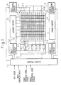
- Fig. 1 is a block diagram showing an overview of the PDP disclosed in the Japanese Unexamined Patent Publication No. 9-160525 .
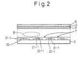
- Fig. 2 shows a sectional structure of the panel.
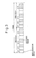
- Fig. 3 is a diagram showing a structure of one frame.
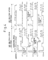
- Fig. 4 is a timing chart showing the waveforms of driving signals applied to electrodes within one sub-field.
- a panel 1 has first electrodes (X electrodes) 2-1, 2-2, etc. and second electrodes (Y electrodes) 3-1, 3-2, etc., which serve as sustaining discharge electrodes, and address electrodes 4-1, 4-2, etc.
- the panel 1 is composed of two glass substrates 5 and 6.
- transparent electrodes 22-1, etc. and bus electrodes 21-1, etc. which constitute the X electrodes
- transparent electrodes 32-1, 32-2, etc. and bus electrodes 31-1, 31-2, etc. which constitute the Y electrodes are arranged in parallel with one another.
- the substrate 5 provides a display surface.
- the transparent electrode is used for the purpose of transmitting light generated at a phosphor 9.
- the bus electrode is employed for the purpose of preventing a voltage drop caused by an electrode resistance. These electrodes are coated with a dielectric. A film made of magnesium oxide (MgO) is formed as a protective film on a discharge surface.
- MgO magnesium oxide
- address electrodes 4 are formed on the glass substrate 6 opposed to the glass substrate 5 so that the address electrodes 4 will be orthogonal to the X and Y electrodes.
- a barrier 10 is formed between adjoining ones of the address electrodes.
- a phosphor 9 exhibiting a characteristic of glowing in red, green, and blue is formed between adjoining ones of the barriers 10 so that the phosphor 9 will cover each address electrode.
- the two glass substrates 5 and 6 are assembled so that the ridges of the barriers 10 will come into close contact with the MgO film.
- Each electrode can be discharged to release a charge to slits 8 defined by electrodes across the electrode.
- the slit 8 which is defined between electrodes and in which discharge occurs for display shall be referred to as a discharge slit.
- the discharge slit coincides with display cells or a line formed by the display cells.
- the Y electrodes are utilized mainly for selecting a display line during an addressing operation and for sustaining discharge.
- the address electrodes are utilized mainly for selecting display cells defined by a Y electrode coincident with the selected display line.
- the X electrodes are utilized mainly for selecting in which of the discharge slits across the Y electrode selected during the addressing operation addressing discharge should be initiated.
- the address electrodes 4-1, 4-2, etc. are connected one by one to an address driver 13.
- the address driver 13 applies an addressing pulse for addressing discharge.
- the Y electrodes are connected individually to a scan driver 12.
- the scan driver 12 is divided into a portion for driving odd X electrodes 4-1, 4-3, etc. and a portion for driving even Y electrodes 4-2, 4-4, etc. in order to deal with the data bit by bit.
- the portions of the scan driver 12 are connected to an odd Y sustaining circuit 16 and even Y sustaining circuit 17.
- a pulse to be applied during an addressing operation is generated by the scan driver 12.
- a sustaining discharge pulse or the like is generated by the odd Y sustaining circuit 16 and even Y sustaining circuit 17, and applied to the Y electrodes by way of the scan driver 12.
- the X electrodes 2-1, 2-2, etc. are grouped into odd X electrodes 2-1, 2-3, etc. and even X electrodes 2-2, 2-4, etc.
- the groups are connected to the odd X sustaining circuit 14 and even X sustaining circuit 15 respectively.
- These drivers are controlled by a control circuit 11.
- the control circuit is controlled with synchronizing (hereinafter sync) signals and a display data signal which are input externally.
- a driving sequence for one frame employed in the PDP is divided into a driving sequence for an odd field and a driving sequence for an even field.
- odd lines are displayed.
- even lines are displayed.
- discharge is initiated in regions defined between an odd-numbered X electrode and odd-numbered Y electrode and a region between an even-numbered X electrode and even-numbered Y electrode.
- discharge is initiated in regions defined between the odd-numbered Y electrode and even-numbered X electrode, and a region between the odd-numbered X electrode and even-numbered Y electrode.
- Each field is divided into several sub-fields. In Fig.
- each field is divided into eight sub-fields SF1, SF2, etc., and SF8.
- Each sub-field is composed of a reset period during which display cells are initialized, an addressing period during which display data is written (addressing), and a sustaining period during which only cells in which a wall charge is produced due to addressing are repeatedly discharged (sustaining discharge).
- addressing discharge and sustaining discharge are initiated for displaying an odd line alone.
- addressing discharge and sustaining discharge are initiated for displaying an even line alone.
- the luminance of display is determined with the length of the sustaining discharge period, that is, the number of sustaining discharge pulses.
- the reset periods and addressing periods thereof have the same lengths.
- the ratio of the lengths of the sustaining discharge periods thereof is 1:2:4:8:16:32:64:128.
- a luminance can be serd in 256 steps ranging from level 0 to level 255.
- Fig. 4 is a timing chart showing the waveforms of driving signals employed in the plasma display device shown in Fig. 1 .
- the driving signals are output during one sub-field.
- one sub-field is divided into a reset/addressing period, and a sustaining discharge period (sustaining period).
- a whole-surface writing pulse of a voltage calculated by adding up voltages Vs and Vw (approximately 300 V) is applied to the X electrodes.
- the reset operation has the effect of bringing all the display cells to the same state irrespective of their being or not being lit during the previous sub-field, and is carried out in order to stabilize subsequent addressing (writing) discharge.
- the addressing period is divided into a first-half addressing period and second-half addressing period. For example, during the first-half addressing period within the odd field, the display cells constituting the first line, fifth line, etc. are addressed. During the second-half addressing period, the display cells constituting the third line, seventh line, etc. are addressed. During the first-half addressing period within the even field, the display cells constituting the second line, sixth line, etc. are addressed. During the second-half addressing period, the display cells constituting the fourth line, eighth line, etc. are addressed.
- a voltage Vx (approximately 50 V) is applied to the first, third, and other odd-numbered X electrodes, and a voltage of 0 V is applied to the second, fourth, and other even-numbered X electrodes.
- a scanning pulse (- VY: - 150 V) is applied to the first, third, and other odd-numbered Y electrodes.
- the voltage of 0 V is applied to the second, fourth, and other even-numbered Y electrodes.
- an addressing pulse of a voltage Va (approximately 50 V) is applied selectively to the address electrodes.
- the voltage Vx (approximately 50 V) is applied to the second, fourth, and other even-numbered X electrodes.
- the voltage of 0 V is applied to the first, third, and other odd-numbered X electrodes.
- the scanning pulse (- VY: - 150 V) is applied sequentially to the second, fourth, and other even-numbered Y electrodes.
- the display cells constituting the third line, seventh line, etc. are addressed.
- addressing the display cells constituting the first, third, fifth, and other odd-numbered lines is completed.
- a sustaining discharge pulse of a voltage Vs (approximately 180 V) is applied alternately to a Y electrode and X electrode. Sustaining discharge is then initiated. An image for one sub-field within the odd field is displayed. At this time, a voltage applied to the odd-numbered X electrode and odd-numbered Y electrode and a voltage applied to the even-numbered X electrode and even-numbered Y electrode are mutually out of phase. A potential difference Vs is therefore produced between the regions defined by an odd-numbered X electrode and odd-numbered Y electrode surrounding an odd-numbered discharge slit, and the regions defined by an even-numbered X electrode and even-numbered Y electrode surrounding an odd-numbered discharge slit.
- Vs approximately 180 V
- the display cells constituting an even-numbered line are dealt with for displaying an image.
- display cells are specified between an Y electrode and X electrodes across the Y electrode.
- the panel has a structure similar to the one of the prior art, the panel can achieve higher-definition display.
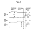
- Fig. 5 is a diagram showing a state attained between the addressing period and sustaining discharge period.
- sustaining discharge pulses that are mutually out of phase are applied alternately to adjoining slits to be involved in display. For example, for initiating discharge in an odd display slit during the odd field, the display cells lying in an odd-numbered one of odd display slits, that is, in the (4n+1)-th (where n denotes an integer equal to or larger than 0) slit are addressed during the first-half addressing period.
- the display cells lying in an even-numbered one of the odd display slits, that is, in the (4n+3)-th (where n denotes an integer equal to or larger than 0) slit are addressed during the second-half addressing period.
- a negative charge is accumulated on an X electrode and a positive charge is accumulated on a Y electrode.
- a low-voltage sustaining discharge pulse is applied to the odd-numbered X electrode
- a high-voltage sustaining discharge pulse is applied to the even-numbered X electrode.
- a high-voltage sustaining discharge pulse is applied to the odd-numbered Y electrode
- a low-voltage sustaining discharge pulse is applied to the even-numbered Y electrode.
- initial sustaining discharge 101 occurs in the odd-numbered one of the odd display slits.
- the sustaining discharge pulses are reversed. Consequently, a high-voltage sustaining discharge pulse is applied to the odd-numbered X electrode, and a low-voltage sustaining discharge pulse is applied to the even-numbered X electrode.
- a low-voltage sustaining discharge pulse is applied to the odd-numbered Y electrode, and a high-voltage sustaining discharge pulse is applied to the even-numbered Y electrode.
- sustaining discharge 102 occurs in the odd-numbered one of the odd display slits.
- Sustaining discharge 103 occurs in the even-numbered one of the odd display slits.
- a sustaining discharge pulse rises first at time instant T0.
- Initial sustaining discharge succeeding addressing is largely delayed.
- sustaining discharge is started at time instant T1.
- sustaining discharge does not occur in an even-numbered odd display slit.
- the polarity of a sustaining discharge pulse is reversed.
- the second sustaining discharge is initiated immediately.
- discharge delayed because it is an initial sustaining discharge.
- Discharge is started at time instant T4.
- the luminance of the PDP depends on the number of sustaining discharge.
- the cycle of a sustaining discharge pulse must be short. Therefore, if the initial sustaining discharge is largely delayed as mentioned above, before the initial sustaining discharge is completed, the polarity of a sustaining discharge pulse is reversed. When this takes place, the movement of a charge between an X electrode and Y electrode deriving from sustaining discharge is not achieved successfully. There is some fear that subsequent sustaining discharge may not be carried out and the normal display may fail.
- a sustaining discharge pulse applied to an adjoining odd discharge slit at the time instant T1 of initial sustaining discharge is opposite in polarity to an accumulated wall charge. Discharge occurring in an odd-numbered odd display slit will not affect the wall charge accumulated in an adjoining even-numbered odd display slit.
- the second sustaining discharge occurs in the odd-numbered odd display slit at time instant T2
- the polarity of a sustaining discharge pulse applied to the even-numbered odd display slit has already been reversed.
- occurrence of initial sustaining discharge in the even-numbered odd display slit is delayed. This poses a problem that the wall charge in the even-numbered odd display slit disappears because of the second sustaining discharge occurring in the odd-numbered odd display slit. When the disappearance of a wall charge takes place, sustaining discharge will not be achieved. Consequently, the normal display fails.
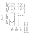
- Fig. 7 is a diagram showing a sequence of driving the plasma display panel (PDP) in accordance with the first embodiment of the present invention.
- the PDP concerned is that of the plasma display device disclosed in Japanese Unexamined Patent Publication No. 9-160525 .
- the fundamental drive method has already been described. Herein, only a difference will be described.
- A denotes addressing discharge.
- T denotes a charge adjustment pulse, and
- S denotes sustaining discharge.
- the other embodiments are also concerned with the PDP. The description of the PDP will be omitted.
- a charge adjustment period is set between the second-half addressing period and sustaining discharge period. Discharge occurring during the charge adjustment period, like sustaining discharge contributes to luminance.
- the charge adjustment period is equivalent to the first part of the sustaining discharge period.
- the charge adjustment pulse to be applied during the charge adjustment period has the same polarity and strength as a sustaining discharge pulse employed the prior art, but has a longer duration than the sustaining discharge pulse.
- the potential at a Y electrode defining an odd display slit rises in the same manner as that in the prior art.
- Initial discharge T111 occurring in the odd display slit delays. The polarity of a sustaining discharge pulse is then reversed.
- the second sustaining discharge 112 is initiated immediately in the odd-numbered odd display slit.
- the discharge since the discharge is initial sustaining discharge, the discharge 113 is delayed.
- the duration of the charge adjustment pulse is long, after the discharge 113 occurs, it takes much time for the charge adjustment pulse to reverse in polarity in response to the next sustaining discharge pulse. The delay in discharge 113 will therefore not be affected by the next sustaining discharge pulse.
- the duration of the charge adjustment pulse to be applied during the charge adjustment period is longer than that of the sustaining discharge pulse, that is, the duration of the initial sustaining discharge pulse is longer. Consequently, it will not occur that initial sustaining discharge is affected by the next sustaining discharge pulse because of a delay. Sustaining discharge can be initiated successfully in all display slits.
- Fig. 8 is a diagram showing a sequence of driving a PDP in accordance with the second embodiment of the present invention.
- the first-half addressing period is succeeded by a charge adjustment period. Only one charge adjustment pulse is applied to an odd-numbered odd display slit. Consequently, charges accumulated on an X electrode and Y electrode defining the odd-numbered odd display slit during the first-half addressing period are exchanged for each other.
- a negative charge is accumulated on an X electrode, and a positive charge is accumulated on the Y electrode.
- the charge adjustment pulse With the charge adjustment pulse, a positive charge is accumulated on the X electrode and a negative charge is accumulated on the Y electrode.
- the charge adjustment pulse is not applied to an even-numbered odd display slit. None occurs in the even-numbered odd display slit. Thereafter, a charge is accumulated on the X electrode and Y electrode defining the even-numbered odd display slit. At this time instant, the polarity of the charges on the X electrode and Y electrode defining the odd-numbered odd display slit is opposite to that of the charges on the X electrode and Y electrode defining the even-numbered odd display slit.
- the sustaining discharge pulse for initiating discharge first in the even-numbered odd display slit is applied as illustrated, sustaining discharge occurs simultaneously in both the odd display slits.
- the duration of a sustaining discharge pulse to be applied first after the second-half addressing period may be made longer than that of the other sustaining discharge pulses.
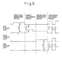
- Fig. 9 is a diagram showing a sequence of driving a PDP in accordance with the third embodiment of the present invention.
- the first-half addressing period is succeeded by a charge adjustment period.
- the potential at an Y electrode is retained at an intermediate level until the second-half addressing period is completed.
- the intermediate level is an appropriate intermediate level between 0 V and the voltage of a sustaining discharge pulse.
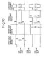
- Fig. 10 is a diagram showing a sequence of driving a PDP in accordance with the fourth embodiment of the present invention.
- a charge adjustment period is set between the.second-half addressing period and sustaining discharge period.
- the polarity of a pulse applied to either the even-numbered or odd-numbered odd display slits is reversed.
- the polarity of the pulse applied to the even-numbered odd display slits is reversed.
- discharge occurs in the even-numbered odd display slit.
- the succeeding sustaining discharge period is identical to that in the prior art.
- application of the charge adjustment pulse leads to application of a voltage causing discharge in an even display slit.
- the polarity of a charge accumulated in the even display slit is opposite to that in an odd display slit, no discharge occurs.
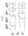
- Fig. 11 is a diagram showing a sequence of driving a PDP in accordance with the fifth embodiment of the present invention.
- a charge adjustment period is set between the second-half addressing period and sustaining discharge period. After initial discharge is initiated separately in odd display slits, the polarities of accumulated charges are adjusted. The sustaining discharge period is then started. Specifically, a charge adjustment pulse is applied to an odd-numbered odd display slit. This initiates initial discharge T1. At this time, a pulse whose polarity is opposite to that of a held charge is applied to an even-numbered odd display slit. Thereafter, a charge adjustment pulse is applied to the even-numbered odd display slit in order to initiate initial discharge T2.
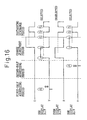
- Fig. 12 is a diagram showing a sequence of driving a PDP in accordance with the sixth embodiment of the present invention.
- This embodiment is similar to the fifth embodiment wherein, when initial discharge T2 is initiated in the even-numbered odd display slit, a voltage to be applied to the odd-numbered odd display slit is set to a low voltage. Thus, the possibility of occurrence of discharge in an even display slit is reduced.
- Fig. 13 is a diagram showing a sequence of driving a PDP in accordance with the seventh embodiment of the present invention.
- This embodiment is similar to the first embodiment, wherein initial discharge is initiated first in an even-numbered odd display slit.
- initial discharge should be initiated first is determined by comparing the magnitude of addressing discharge occurring in the odd-numbered odd display slit with the one occurring in the even-numbered odd display slit in advance.
- Discharge is initiated first in a display slit in which a smaller magnitude of addressing discharge has occurred.
- the magnitude of addressing discharge differs between the odd-numbered and even-numbered odd display slits. The same applies to even display slits.
- Fig. 14 is a diagram showing a sequence of driving a PDP in accordance with the eighth embodiment of the present invention.
- Fig. 15 is a diagram for explaining the principles of selecting a slit in the eighth embodiment.
- a discharge slit is selected depending on which of the potentials at odd-numbered and even-numbered X electrodes is higher.
- the selection is carried out during the charge adjustment period.
- the potential at an X electrode is retained at 0 V during the first-half addressing period and second-half addressing period.
- a scanning pulse is applied to a Y electrode, and an addressing pulse is applied to an address electrode.
- addressing discharge is initiated.
- either of an odd display slit and even display slit is selected as a slit in which discharge is initiated. Specifically, discharge is initiated in a slit to which a charge adjustment pulse of the same polarity as a charge accumulated on the Y electrode has been applied. No discharge is initiated in a slit to which a charge adjustment pulse of opposite polarity has been applied. In the drawing, an odd-numbered odd display slit is discharged with the first charge adjustment pulse. An even-numbered odd display slit is discharged with the next charge adjustment pulse. Thus, the odd display slits are selected.
- the potentials at electrodes Y1 and X2 are set to a high potential lower than a discharge start voltage, and the potentials at electrodes X1 and Y2 are set to 0 V.
- a positive charge is added to the potential at the electrode Y1.
- the potential at the electrode Y1 therefore exceeds the threshold of the discharge start voltage.
- Discharge is then initiated in the regions between the electrodes X1 and Y1.
- the potentials at the other electrodes do not exceed the threshold of the discharge start voltage. Discharge will therefore not occur.
- the potentials at the electrodes X1 and Y2 are set to a high potential lower than the discharge start voltage, and the potentials at the electrode X2 and Y1 are set to 0 V. Discharge is then initiated in the regions between the electrodes X2 and Y2.
- an odd display slit is selected.
- Fig. 16 is a diagram showing a sequence of driving a PDP in accordance with the ninth embodiment of the present invention.
- the voltage of a charge adjustment pulse to be applied during the charge adjustment period is higher than that in the eighth embodiment.
- addressing discharge is limited to an opposed discharge that is discharge initiated in the regions defined between an Y electrode and address electrode. The produced wall charge is therefore small and sustaining discharge hardly occurs.
- the voltage of the charge adjustment pulse is made high enough to initiate initial discharge. Once discharge occurs, subsequent sustaining discharge pulses may have the voltage conventionally adopted.
- Fig. 17 is a diagram showing a sequence of driving a PDP in accordance with a first other drive method for a PDP as in fig. 1 and 2
- this drive method the number of glows occurring in a slit in which display cells are addressed during the first-half addressing period agrees with the number of glows occurring in a slit in which display cells are addressed during the second-half addressing period.
- a frequency adjustment pulse is applied after the completion of the sustaining discharge period so that discharge will be initiated only in a slit in which sustaining discharge has occurred a small number of times. Consequently, the frequencies of glow occurring in both the slits agree with each other.
- the frequency of discharge occurring in an odd-numbered odd display slit during the sustaining discharge period is four times.
- the frequency of discharge occurring in an even-numbered odd display slit is three times.
- a frequency adjustment pulse 201 is applied to the even-numbered odd display slit.
- discharge is initiated in the even-numbered odd display slit alone.
- a voltage is applied to even display slits.
- no discharge occurs.
- Fig. 18 is a diagram showing a sequence of driving a PDP in accordance with a second other drive method for a PDP as in fig. 1 and 2 .
- application of the frequency adjustment pulse 201 is preceded by a remaining charge adjustment period.
- the remaining charge adjustment period is a period coincident with the long duration of the last pulse that used to be applied during the sustaining-discharge period. Owing to the remaining charge adjustment period, disappearance of a charge or incorrect writing deriving from the adverse effect of sustaining discharge upon a display slit in which discharge is not initiated can be overcome. Eventually, a reset can be carried out satisfactorily.
- Fig. 19 is a diagram showing a sequence of driving a PDP in accordance with a third other drive method for a PDP as in fig. 1 and 2 .
- this drive method when the frequency adjustment pulse 201 is applied to one slit in which discharge has occurred by a smaller number of times, according to the first other drive method, a pulse for preventing loss of a charge is applied to the other slit. This results in satisfactory erase at the subsequent erasing step.
- Fig. 20 is a diagram showing a sequence of driving a PDP in accordance with a fourth other drive method for a PDP as in fig. 1 and 2 .
- this drive method when the frequency adjustment pulse is applied to one slit, in which discharge has occurred by a smaller number of times, according to the first other drive method, a pulse 205 for preventing loss of a charge and lowering the voltage of charges in another slits is applied to the other slit.
- a high voltage is applied to an X electrode defining an even-numbered odd display slit, and 0 V is applied to a Y electrode defining it.
- a high voltage is applied to an X electrode defining an odd-numbered odd display slit, and an intermediate voltage is applied to a Y electrodes defining it. Consequently, a charge in the odd-numbered odd display slit is held reliably. Occurrence of discharge in an even display slit can be reliably prevented.
- a drive method for high-definition plasma display panels in which sustaining discharge pulses that are mutually out of phase are applied to adjoining slits in order to initiate sustaining discharge and to thus specify display slits between an Y electrode and X electrodes across the Y electrode.
- a normal display can be achieved on a stable basis.
Landscapes
- Engineering & Computer Science (AREA)
- Physics & Mathematics (AREA)
- Power Engineering (AREA)
- Plasma & Fusion (AREA)
- Computer Hardware Design (AREA)
- General Physics & Mathematics (AREA)
- Theoretical Computer Science (AREA)
- Control Of Indicators Other Than Cathode Ray Tubes (AREA)
- Control Of Gas Discharge Display Tubes (AREA)
Description
- The present invention relates to a technology for driving a display panel composed of a set of cells that are display elements possessing a memory function. More particularly, this invention is concerned with a device for displaying an image on an alternating current (AC) type plasma display panel (PDP) with interlaced scanning.
- In the AC type PDP, a voltage waveform is applied alternately to two sustaining electrodes in order to sustain discharge and emit light for display. One discharge is completed in one to several microseconds immediately after application of a pulse. Positively charged ions stemming from the discharge are accumulated on the surface of an insulating layer over electrodes to which a negative voltage has been applied. Likewise, electrons carrying negative charges are accumulated on the surface of the insulating layer over electrodes to which a positive voltage has been applied.
- First, discharge is initiated with a pulse (writing pulse) of a high voltage (writing voltage) in order to produce a wall charge. Thereafter, a pulse (sustaining discharge pulse) of a voltage (sustaining discharge voltage) lower than the previous voltage is applied. The previously accumulated wall charge is then added to the voltage. The voltage becomes high relative to the potential in the discharge space and exceeds the threshold of a discharge voltage. Consequently, discharge is started. In other words, once a display cell is discharged for writing, when sustaining discharge pulses of opposite polarities are applied alternately, the display cell in which a wall charge has been produced sustains discharge. This property of a display cell is referred to as a memory effect or memory function. In general, the AC type PDP utilizes the memory effect to carry out display.
- In an AC type PDP of a prior art, X electrodes that are one group of sustaining electrodes and Y electrodes that are the other group thereof are arranged alternately. Discharge is initiated in regions defined between odd-numbered X electrodes and odd-numbered Y electrodes, and in regions defined between even-numbered X electrodes and even-numbered Y electrodes. In other words, display cells are defined between odd-numbered X electrodes and odd-numbered Y electrodes, and between even-numbered X electrodes and even-numbered Y electrodes. No display cells are defined between odd-numbered Y electrodes and even-numbered X electrodes, and between odd-numbered X electrodes and even-numbered Y electrodes. However, this poses a problem that it is hard to attain high definition and high luminance. The present inventor has disclosed a PDP in Japanese Unexamined Patent Publication No.
9-160525 9-160525 - In the PDP disclosed in the Japanese Unexamined Patent Publication No.
9-160525 - The luminance of a PDP depends on the frequency of sustaining discharge. For realizing a high-luminance PDP, the cycle of a sustaining discharge pulse must be short. However, as mentioned above, if an initial sustaining discharge is largely delayed, before the initial sustaining discharge is completed, the polarity of a sustaining discharge pulse is reversed. When this occurs, movement of charges between an X electrode and Y electrode deriving from sustaining discharge is not sufficiently achieved. There is a fear that subsequent sustaining discharge may not be carried out. Consequently, a normal display fails.
- Moreover, the polarity of a sustaining discharge pulse applied to adjacent odd discharge slits at the time of initial sustaining discharge is opposite to that of an accumulated wall charge. A discharge occurring in an odd-numbered odd display slit will not affect a wall charge in an even-numbered odd display slit. However, when the second sustaining discharge occurs in the odd-numbered odd display slit at time instant, the polarity of a sustaining discharge pulse applied to the even-numbered odd display slit has already been reversed. Moreover, occurrence of initial sustaining discharge in the even-numbered odd display slit is delayed. This poses a problem that the wall charge in the even-numbered odd display slit disappears because of the second sustaining discharge occurring in the odd-numbered odd display slit in the meantime. When the disappearance of a wall charge occurs, sustaining discharge is not carried out. Consequently, a normal display fails.
- Furthermore, during the sustaining discharge period, there is a difference of one time between the number of glows in a slit to be addressed during the first-half addressing period and the number of glows in a slit to be addressed during the second-half addressing period. The number of glows within a sub-field that is weighted a little is several times. Even the difference of one time therefore leads to a problem on gray-scale display.
- Moreover, there is a problem that erase to be carried out at an erasing step succeeding the sustaining discharge period is achieved imperfectly depending on the magnitude or polarity of a charge on an electrode.
- It is desirable to provide a drive method that ensures normal display, on a stable basis, in a plasma display panel in which sustaining discharge pulses that are mutually out of phase are applied to adjoining slits in order to initiate sustaining discharge and to thus specify display slits between a Y electrode and X electrodes across the Y electrode.
- An example of related prior art is provided by a drive method for a plasma display device disclosed in the Japanese Unexamined Patent Publication No.
9-160525 - The plasma display device of the present invention has a display panel including first and second electrodes arranged to be parallel with one another, and third electrodes arranged to be orthogonal to the first and second electrodes. In the plasma display device, a slit coincident with a line formed by discharge cells is selected by respectively applying a scanning pulse and an addressing signal to second and third electrodes during an addressing step. Sustain discharge is initiated in the selected slit by applying sustaining discharge pulses to the first and second electrodes during a sustaining discharge step. According to the drive method, sustaining discharge pulses that are mutually out of phase are applied alternately to adjoining ones of the first electrodes and adjoining ones of the second electrodes. Consequently, a first slit is defined between a second electrode and a first electrode located on one side of the second electrode, and a second slit is defined between the second electrode and a first electrode located on the other side of the second electrode. Interlacing is carried out by repeating glows alternately in the first slit and second slit for display. The drive method of the plasma display device is characterized in that a charge adjustment step is set between the addressing step and sustaining discharge step. During the charge adjustment step, a charge adjustment pulse is applied in order to adjust at least one of the polarity and magnitude of a wall charge accumulated due to discharge occurring at the addressing step.
- To assist in preventing imperfect sustaining discharge derived from a delay in initial discharge succeeding the addressing step, a charge adjustment pulse whose duration is longer than the duration of a sustaining discharge pulse is preferably applied.
- The charge adjustment step may be effected both after the first-half addressing step and after the second-half addressing step. In this case, a state in which a charge adjustment pulse that is opposite in polarity to a wall charge produced during the addressing step has been applied should preferably be retained during a period after the completion of the addressing step until the sustaining discharge step is started.
- To prevent a wall charge in one discharge slit from disappearing because of the second discharge occurring in the other discharge slit in which sustaining discharge occurs first, various approaches are conceivable. For example, a charge adjustment pulse for starting discharge may be applied simultaneously to slits selected during the first-half addressing step and the second-half addressing step. Moreover, a charge adjustment pulse may be applied to the slits selected during the first-half addressing step and the second-half addressing step so that discharge will be started at different time instants. In this case, a charge adjustment pulse that is opposite in polarity to a wall charge produced during the addressing step and a wall charge produced with a charge adjustment pulse, and has a small difference in voltage from the wall charges, is applied to slits other than the slit in which discharge is initiated.
- Moreover, the degree of accumulation of a wall charge deriving from discharge occurring during the first-half addressing step can be compared with the degree of accumulation of a wall charge deriving from discharge occurring during the second-half addressing step in advance. In this case, during the charge adjustment step, a charge adjustment pulse is applied so that a slit having a smaller wall charge will be discharged first. This ensures a more reliable occurrence of sustaining discharge.
- Furthermore, selecting a discharge slit need not be carried out during the addressing step but can be carried out during the charge adjustment step. In this case, an equal voltage is applied to the first electrodes during the addressing step. The charge adjustment pulse is used to select either of the first and second slits as a slit coincident with a line to be displayed. Discharge occurring during the addressing step involves the second and third electrodes alone. During the charge adjustment step, a charge adjustment pulse is applied in order to select to which of second electrodes defining adjoining slits the charge accumulated on the second electrode should be moved. In this case, a voltage to which a dielectric layer formed over the third electrodes should be set is set to a low voltage. Thus, a charge sufficient to initiate sustaining discharge can be produced during addressing. Moreover, the voltage of the charge adjustment pulse should preferably be set to a value larger than the voltage of the sustaining discharge pulse.
- Another drive method of plasma display panels suitable for use with a plasma display device as disclosed in the Japanese Unexamined Patent Publication No.
9-160525 - Furthermore, still another drive method for plasma display panels suitable for use with a plasma display device as disclosed in the Japanese Unexamined Patent Publication No.
9-160525 - In the latter two examples of drive methods for plasma display panels, the duration of a sustaining discharge pulse to be applied immediately before application of a remaining charge adjustment pulse should preferably be longer than the duration of a sustaining discharge pulse. Moreover, a pulse that is opposite in polarity to charge accumulated during the sustaining discharge step should desirably be applied to slits other than a slit in which discharge is initiated with the remaining charge adjustment pulse. Besides, a voltage that is lower than a voltage to be applied to the slit in which discharge is initiated should preferably be applied to the slits other than the slit in which discharge is initiated with the remaining charge adjustment pulse.
- The above mentioned drive methods can be provided by a corresponding drive circuitry.
- Reference will now be made, by way of example, to the accompanying drawings, in which:
-
Fig. 1 is a block diagram showing a configuration of a plasma display panel (PDP) to which embodiments of the present invention can be applied; -
Fig. 2 is a diagram showing a sectional structure of the panel shown inFig. 1 ; -
Fig. 3 is a diagram showing a structure of a display frame employed in the PDP shown inFig. 1 ; -
Fig. 4 is a timing chart showing the waveforms of driving signals employed in the PDP shown inFig. 1 ; -
Fig. 5 is a diagram for explaining an underlying problem of a prior art PDP drive method; -
Fig. 6 is a diagram for explaining an underlying problem of the prior art PDP drive method; -
Fig. 7 is a timing chart showing the waveforms of driving signals employed in the first embodiment of the present invention; -
Fig. 8 is a timing chart showing the waveforms of driving signals employed in the second embodiment of the present invention; -
Fig. 9 is a timing chart showing the waveforms of driving signals employed in the third embodiment of the present invention; -
Fig. 10 is a timing chart showing the waveforms of driving signals employed in the fourth embodiment of the present invention; -
Fig. 11 is a timing chart showing the waveforms of driving signals employed in the fifth embodiment of the present invention; -
Fig. 12 is a timing chart showing the waveforms of driving signals employed in the sixth embodiment of the present invention; -
Fig. 13 is a timing chart showing the waveforms of driving signals employed in the seventh embodiment of the present invention; -
Fig. 14 is a timing chart showing the waveforms of driving signals employed in the eighth embodiment of the present invention; -
Fig. 15 is a diagram for explaining the operations of the eighth embodiment; -
Fig. 16 is a timing chart showing the waveforms of driving signals employed in the ninth embodiment of the present invention; -
Fig. 17 is a timing chart showing the waveforms of driving signals employed in a first other drive method for a PDP as infig. 1 and2 ; -
Fig. 18 is a timing chart showing the waveforms of driving signals employed in a second other drive method for a PDP as infig. 1 and2 ; -
Fig. 19 is a timing chart showing the waveforms of driving signals employed in a third other drive method for a PDP as infig. 1 and2 ; and -
Fig. 20 is a timing chart showing the waveforms of driving signals employed in a fourth other drive method for a PDP as infig. 1 and2 . - Before proceeding to a detailed description of the preferred embodiments, a prior art plasma display panel and drive method thereof, as disclosed in the Japanese Unexamined Patent Publication No.
9-160525 -
Fig. 1 is a block diagram showing an overview of the PDP disclosed in the Japanese Unexamined Patent Publication No.9-160525 Fig. 2 shows a sectional structure of the panel.Fig. 3 is a diagram showing a structure of one frame.Fig. 4 is a timing chart showing the waveforms of driving signals applied to electrodes within one sub-field. Referring to these drawings, an example of one PDP to which the present invention can be applied will be described below - As shown in
Fig. 1 , apanel 1 has first electrodes (X electrodes) 2-1, 2-2, etc. and second electrodes (Y electrodes) 3-1, 3-2, etc., which serve as sustaining discharge electrodes, and address electrodes 4-1, 4-2, etc. As shown inFig. 2 , thepanel 1 is composed of twoglass substrates 5 and 6. On the first substrate 6, transparent electrodes 22-1, etc. and bus electrodes 21-1, etc. which constitute the X electrodes, and transparent electrodes 32-1, 32-2, etc. and bus electrodes 31-1, 31-2, etc. which constitute the Y electrodes are arranged in parallel with one another. Thesubstrate 5 provides a display surface. The transparent electrode is used for the purpose of transmitting light generated at a phosphor 9. However, the employment of only the transparent electrode results in a large voltage drop. The bus electrode is employed for the purpose of preventing a voltage drop caused by an electrode resistance. These electrodes are coated with a dielectric. A film made of magnesium oxide (MgO) is formed as a protective film on a discharge surface. - Moreover, address electrodes 4 are formed on the glass substrate 6 opposed to the
glass substrate 5 so that the address electrodes 4 will be orthogonal to the X and Y electrodes. Moreover, abarrier 10 is formed between adjoining ones of the address electrodes. A phosphor 9 exhibiting a characteristic of glowing in red, green, and blue is formed between adjoining ones of thebarriers 10 so that the phosphor 9 will cover each address electrode. The twoglass substrates 5 and 6 are assembled so that the ridges of thebarriers 10 will come into close contact with the MgO film. - Each electrode can be discharged to release a charge to
slits 8 defined by electrodes across the electrode. In this specification, theslit 8 which is defined between electrodes and in which discharge occurs for display shall be referred to as a discharge slit. In other words, the discharge slit coincides with display cells or a line formed by the display cells. The Y electrodes are utilized mainly for selecting a display line during an addressing operation and for sustaining discharge. The address electrodes are utilized mainly for selecting display cells defined by a Y electrode coincident with the selected display line. The X electrodes are utilized mainly for selecting in which of the discharge slits across the Y electrode selected during the addressing operation addressing discharge should be initiated. - As shown in
Fig. 1 , the address electrodes 4-1, 4-2, etc. are connected one by one to anaddress driver 13. Theaddress driver 13 applies an addressing pulse for addressing discharge. Moreover, the Y electrodes are connected individually to ascan driver 12. Thescan driver 12 is divided into a portion for driving odd X electrodes 4-1, 4-3, etc. and a portion for driving even Y electrodes 4-2, 4-4, etc. in order to deal with the data bit by bit. The portions of thescan driver 12 are connected to an oddY sustaining circuit 16 and evenY sustaining circuit 17. A pulse to be applied during an addressing operation is generated by thescan driver 12. A sustaining discharge pulse or the like is generated by the oddY sustaining circuit 16 and evenY sustaining circuit 17, and applied to the Y electrodes by way of thescan driver 12. The X electrodes 2-1, 2-2, etc. are grouped into odd X electrodes 2-1, 2-3, etc. and even X electrodes 2-2, 2-4, etc. The groups are connected to the oddX sustaining circuit 14 and even X sustainingcircuit 15 respectively. These drivers are controlled by a control circuit 11. The control circuit is controlled with synchronizing (hereinafter sync) signals and a display data signal which are input externally. - As shown in
Fig. 3 , a driving sequence for one frame employed in the PDP is divided into a driving sequence for an odd field and a driving sequence for an even field. During the odd field, odd lines are displayed. During the even field, even lines are displayed. In other words, during the odd field, discharge is initiated in regions defined between an odd-numbered X electrode and odd-numbered Y electrode and a region between an even-numbered X electrode and even-numbered Y electrode. During the even field, discharge is initiated in regions defined between the odd-numbered Y electrode and even-numbered X electrode, and a region between the odd-numbered X electrode and even-numbered Y electrode. Each field is divided into several sub-fields. InFig. 3 , each field is divided into eight sub-fields SF1, SF2, etc., and SF8. Each sub-field is composed of a reset period during which display cells are initialized, an addressing period during which display data is written (addressing), and a sustaining period during which only cells in which a wall charge is produced due to addressing are repeatedly discharged (sustaining discharge). During the odd field, addressing discharge and sustaining discharge are initiated for displaying an odd line alone. During the even field, addressing discharge and sustaining discharge are initiated for displaying an even line alone. The luminance of display is determined with the length of the sustaining discharge period, that is, the number of sustaining discharge pulses. - In the sub-fields SF1, SF2, etc., and SF8, the reset periods and addressing periods thereof have the same lengths. The ratio of the lengths of the sustaining discharge periods thereof is 1:2:4:8:16:32:64:128. Depending on which of the sub-fields are selected as sub-fields during which a display cell is lit, a luminance can be serd in 256 steps ranging from level 0 to level 255.
-
Fig. 4 is a timing chart showing the waveforms of driving signals employed in the plasma display device shown inFig. 1 . The driving signals are output during one sub-field. In this example, one sub-field is divided into a reset/addressing period, and a sustaining discharge period (sustaining period). During the reset period, first, all the Y electrodes are set to 0 V. At the same time, a whole-surface writing pulse of a voltage calculated by adding up voltages Vs and Vw (approximately 300 V) is applied to the X electrodes. The reset operation has the effect of bringing all the display cells to the same state irrespective of their being or not being lit during the previous sub-field, and is carried out in order to stabilize subsequent addressing (writing) discharge. - Thereafter, during the addressing period, addressing discharge is carried out line-sequentially in order to turn on or off the display cells according to display data. In a conventional PDP, the same voltage is applied to all X electrodes and a scanning pulse is applied sequentially to Y electrodes. However, the PDP shown in
Fig. 1 operates differently. The addressing period is divided into a first-half addressing period and second-half addressing period. For example, during the first-half addressing period within the odd field, the display cells constituting the first line, fifth line, etc. are addressed. During the second-half addressing period, the display cells constituting the third line, seventh line, etc. are addressed. During the first-half addressing period within the even field, the display cells constituting the second line, sixth line, etc. are addressed. During the second-half addressing period, the display cells constituting the fourth line, eighth line, etc. are addressed. - To begin with, during the first-half addressing period within the odd field, a voltage Vx (approximately 50 V) is applied to the first, third, and other odd-numbered X electrodes, and a voltage of 0 V is applied to the second, fourth, and other even-numbered X electrodes. A scanning pulse (- VY: - 150 V) is applied to the first, third, and other odd-numbered Y electrodes. At this time, the voltage of 0 V is applied to the second, fourth, and other even-numbered Y electrodes. Besides, an addressing pulse of a voltage Va (approximately 50 V) is applied selectively to the address electrodes. Consequently, discharge occurs in the regions of display cells, which are to be lit, defined between an address electrode and Y electrode. Immediately thereafter, the regions thereof defined between an X electrode and the Y electrode are discharged with the discharge as priming. The voltage Vx is applied to the odd-numbered X electrodes and the voltage of 0 V is applied to the even-numbered X electrodes. The discharge is therefore initiated in a discharge slit by the side of an X electrode to which the voltage Vx has been applied. Consequently, a wall charge permitting occurrence of sustaining discharge is accumulated on the MgO film over the X electrode and Y electrode defining the selected cells constituting the selected line. When the foregoing operation is carried out until the last Y electrode is involved, the display cells constituting the first line, fifth line, etc. are addressed.
- Thereafter, during the second-half addressing period within the odd field, the voltage Vx (approximately 50 V) is applied to the second, fourth, and other even-numbered X electrodes. The voltage of 0 V is applied to the first, third, and other odd-numbered X electrodes. The scanning pulse (- VY: - 150 V) is applied sequentially to the second, fourth, and other even-numbered Y electrodes. Thus, the display cells constituting the third line, seventh line, etc. are addressed. During the first-half and second-half addressing periods within the odd field, addressing the display cells constituting the first, third, fifth, and other odd-numbered lines is completed.
- Thereafter, during the sustaining discharge period, a sustaining discharge pulse of a voltage Vs (approximately 180 V) is applied alternately to a Y electrode and X electrode. Sustaining discharge is then initiated. An image for one sub-field within the odd field is displayed. At this time, a voltage applied to the odd-numbered X electrode and odd-numbered Y electrode and a voltage applied to the even-numbered X electrode and even-numbered Y electrode are mutually out of phase. A potential difference Vs is therefore produced between the regions defined by an odd-numbered X electrode and odd-numbered Y electrode surrounding an odd-numbered discharge slit, and the regions defined by an even-numbered X electrode and even-numbered Y electrode surrounding an odd-numbered discharge slit. However, the potential difference Vs will not be produced between the regions defined by an odd-numbered X electrode and an even-numbered Y electrode surrounding an even-numbered discharge slit, and the regions defined by an even-numbered X electrode and an odd-numbered Y electrode surrounding an even-numbered discharge slit. Thus, sustaining discharge is initiated only in the display cells constituting an odd-numbered line.
- Likewise, during the even field, the display cells constituting an even-numbered line are dealt with for displaying an image. As mentioned above, display cells are specified between an Y electrode and X electrodes across the Y electrode. Although the panel has a structure similar to the one of the prior art, the panel can achieve higher-definition display.
- As mentioned above, in the PDP disclosed in the Japanese Unexamined Patent Publication No.
9-160525 Fig. 5 is a diagram showing a state attained between the addressing period and sustaining discharge period. - As shown in
Fig. 5 , according to the prior art, after the second-half addressing period is completed, all the X electrodes and Y electrodes are temporarily set to a zero level. Thereafter, sustaining discharge pulses that are mutually out of phase are applied alternately to adjoining slits to be involved in display. For example, for initiating discharge in an odd display slit during the odd field, the display cells lying in an odd-numbered one of odd display slits, that is, in the (4n+1)-th (where n denotes an integer equal to or larger than 0) slit are addressed during the first-half addressing period. The display cells lying in an even-numbered one of the odd display slits, that is, in the (4n+3)-th (where n denotes an integer equal to or larger than 0) slit are addressed during the second-half addressing period. Thus, a negative charge is accumulated on an X electrode and a positive charge is accumulated on a Y electrode. During the sustaining discharge period, a low-voltage sustaining discharge pulse is applied to the odd-numbered X electrode, and a high-voltage sustaining discharge pulse is applied to the even-numbered X electrode. A high-voltage sustaining discharge pulse is applied to the odd-numbered Y electrode, and a low-voltage sustaining discharge pulse is applied to the even-numbered Y electrode. Accordingly, initial sustainingdischarge 101 occurs in the odd-numbered one of the odd display slits. Thereafter, the sustaining discharge pulses are reversed. Consequently, a high-voltage sustaining discharge pulse is applied to the odd-numbered X electrode, and a low-voltage sustaining discharge pulse is applied to the even-numbered X electrode. A low-voltage sustaining discharge pulse is applied to the odd-numbered Y electrode, and a high-voltage sustaining discharge pulse is applied to the even-numbered Y electrode. Accordingly, sustainingdischarge 102 occurs in the odd-numbered one of the odd display slits. Sustainingdischarge 103 occurs in the even-numbered one of the odd display slits. Thus, depending on which polarity a sustaining discharge pulse to be applied first during the sustaining discharge period has, it is determined in which of the odd-numbered one and even-numbered one of the odd display slits coincident with a line to be displayed sustaining discharge should be started first. In the other slits, start of sustaining discharge is delayed. The same applies to even display slits. An example of displaying a line coincident with an odd display slit during the odd field will be described below. - An adverse effect of a delay in start of sustaining discharge will be described with reference to
Fig. 6 . As mentioned above, a sustaining discharge pulse rises first at time instant T0. Initial sustaining discharge succeeding addressing is largely delayed. In an odd-numbered odd display slit, sustaining discharge is started at time instant T1. At this time, sustaining discharge does not occur in an even-numbered odd display slit. At time instant T2, the polarity of a sustaining discharge pulse is reversed. In the odd-numbered odd display slit, the second sustaining discharge is initiated immediately. However, in the even-numbered odd display slit, discharge delayed because it is an initial sustaining discharge. Discharge,is started at time instant T4. - The luminance of the PDP depends on the number of sustaining discharge. For realizing a high-luminance PDP, the cycle of a sustaining discharge pulse must be short. Therefore, if the initial sustaining discharge is largely delayed as mentioned above, before the initial sustaining discharge is completed, the polarity of a sustaining discharge pulse is reversed. When this takes place, the movement of a charge between an X electrode and Y electrode deriving from sustaining discharge is not achieved successfully. There is some fear that subsequent sustaining discharge may not be carried out and the normal display may fail.
- Moreover, a sustaining discharge pulse applied to an adjoining odd discharge slit at the time instant T1 of initial sustaining discharge is opposite in polarity to an accumulated wall charge. Discharge occurring in an odd-numbered odd display slit will not affect the wall charge accumulated in an adjoining even-numbered odd display slit. However, when the second sustaining discharge occurs in the odd-numbered odd display slit at time instant T2, the polarity of a sustaining discharge pulse applied to the even-numbered odd display slit has already been reversed. Moreover, occurrence of initial sustaining discharge in the even-numbered odd display slit is delayed. This poses a problem that the wall charge in the even-numbered odd display slit disappears because of the second sustaining discharge occurring in the odd-numbered odd display slit. When the disappearance of a wall charge takes place, sustaining discharge will not be achieved. Consequently, the normal display fails.
- As shown in
Fig. 5 , during the sustaining discharge period, there is a difference of one time between the number of glows occurring in a slit to be addressed during the first-half addressing period and the number of glows occurring in a slit to be addressed during the second-half addressing period. The number of glows during a sub-field of low weight is several times. Even the difference of one time poses a problem on gray-scale display. - Moreover, at the erasing step succeeding the sustaining discharge period, there is a problem that erasing is achieved imperfectly depending on the magnitude and polarity of a charge accumulated on an electrode.
-
Fig. 7 is a diagram showing a sequence of driving the plasma display panel (PDP) in accordance with the first embodiment of the present invention. The PDP concerned is that of the plasma display device disclosed in Japanese Unexamined Patent Publication No.9-160525 - As apparent from the comparison with
Fig. 5 , a charge adjustment period is set between the second-half addressing period and sustaining discharge period. Discharge occurring during the charge adjustment period, like sustaining discharge contributes to luminance. The charge adjustment period is equivalent to the first part of the sustaining discharge period. As illustrated, the charge adjustment pulse to be applied during the charge adjustment period has the same polarity and strength as a sustaining discharge pulse employed the prior art, but has a longer duration than the sustaining discharge pulse. By applying such a charge adjustment pulse, the potential at a Y electrode defining an odd display slit rises in the same manner as that in the prior art. Initial discharge T111 occurring in the odd display slit delays. The polarity of a sustaining discharge pulse is then reversed. The second sustainingdischarge 112 is initiated immediately in the odd-numbered odd display slit. However, in an even-numbered odd display slit, since the discharge is initial sustaining discharge, thedischarge 113 is delayed. However, since the duration of the charge adjustment pulse is long, after thedischarge 113 occurs, it takes much time for the charge adjustment pulse to reverse in polarity in response to the next sustaining discharge pulse. The delay indischarge 113 will therefore not be affected by the next sustaining discharge pulse. - As mentioned above, the duration of the charge adjustment pulse to be applied during the charge adjustment period is longer than that of the sustaining discharge pulse, that is, the duration of the initial sustaining discharge pulse is longer. Consequently, it will not occur that initial sustaining discharge is affected by the next sustaining discharge pulse because of a delay. Sustaining discharge can be initiated successfully in all display slits.
-
Fig. 8 is a diagram showing a sequence of driving a PDP in accordance with the second embodiment of the present invention. According to this embodiment, the first-half addressing period is succeeded by a charge adjustment period. Only one charge adjustment pulse is applied to an odd-numbered odd display slit. Consequently, charges accumulated on an X electrode and Y electrode defining the odd-numbered odd display slit during the first-half addressing period are exchanged for each other. In other words, during addressing, a negative charge is accumulated on an X electrode, and a positive charge is accumulated on the Y electrode. With the charge adjustment pulse, a positive charge is accumulated on the X electrode and a negative charge is accumulated on the Y electrode. At this time, the charge adjustment pulse is not applied to an even-numbered odd display slit. Nothing occurs in the even-numbered odd display slit. Thereafter, a charge is accumulated on the X electrode and Y electrode defining the even-numbered odd display slit. At this time instant, the polarity of the charges on the X electrode and Y electrode defining the odd-numbered odd display slit is opposite to that of the charges on the X electrode and Y electrode defining the even-numbered odd display slit. When the sustaining discharge pulse for initiating discharge first in the even-numbered odd display slit is applied as illustrated, sustaining discharge occurs simultaneously in both the odd display slits. - Similarly to the first embodiment, the duration of a sustaining discharge pulse to be applied first after the second-half addressing period may be made longer than that of the other sustaining discharge pulses. Thus, the adverse effect of the delay in initial sustaining discharge to be initiated in the even-numbered odd display slit can be nullified.
-
Fig. 9 is a diagram showing a sequence of driving a PDP in accordance with the third embodiment of the present invention. According to this embodiment, similarly to the second embodiment, the first-half addressing period is succeeded by a charge adjustment period. Moreover, after a charge adjustment pulse is applied to an odd-numbered odd display slit, the potential at an Y electrode is retained at an intermediate level until the second-half addressing period is completed. Thus, a charge accumulated in the odd-numbered odd display slit can be prevented from disappearing during the second-half addressing period. Incidentally, the intermediate level is an appropriate intermediate level between 0 V and the voltage of a sustaining discharge pulse. -
Fig. 10 is a diagram showing a sequence of driving a PDP in accordance with the fourth embodiment of the present invention. According to this embodiment, a charge adjustment period is set between the.second-half addressing period and sustaining discharge period. After a charge adjustment pulse for initiating discharge simultaneously in both even-numbered and odd-numbered odd display slits is applied, the polarity of a pulse applied to either the even-numbered or odd-numbered odd display slits is reversed. In the drawing, the polarity of the pulse applied to the even-numbered odd display slits is reversed. At the time of reversing the polarity, discharge occurs in the even-numbered odd display slit. The succeeding sustaining discharge period is identical to that in the prior art. - According to the fourth embodiment, application of the charge adjustment pulse leads to application of a voltage causing discharge in an even display slit. However, since the polarity of a charge accumulated in the even display slit is opposite to that in an odd display slit, no discharge occurs.
-
Fig. 11 is a diagram showing a sequence of driving a PDP in accordance with the fifth embodiment of the present invention. According to this embodiment, a charge adjustment period is set between the second-half addressing period and sustaining discharge period. After initial discharge is initiated separately in odd display slits, the polarities of accumulated charges are adjusted. The sustaining discharge period is then started. Specifically, a charge adjustment pulse is applied to an odd-numbered odd display slit. This initiates initial discharge T1. At this time, a pulse whose polarity is opposite to that of a held charge is applied to an even-numbered odd display slit. Thereafter, a charge adjustment pulse is applied to the even-numbered odd display slit in order to initiate initial discharge T2. When the discharge T2 is initiated, no charge adjustment pulse is applied to the odd-numbered odd display slit. Discharge therefore does not occur in the odd-numbered odd display slit. The charge in the even-numbered odd display slit will not disappear. Thereafter, the polarity of the pulse applied to the odd-numbered odd display slit is reversed. The normal sustaining discharge period is then started. Thus, initial discharge is initiated separately in both the odd display slits. Disappearance of a charge will not take place. -
Fig. 12 is a diagram showing a sequence of driving a PDP in accordance with the sixth embodiment of the present invention. This embodiment is similar to the fifth embodiment wherein, when initial discharge T2 is initiated in the even-numbered odd display slit, a voltage to be applied to the odd-numbered odd display slit is set to a low voltage. Thus, the possibility of occurrence of discharge in an even display slit is reduced. -
Fig. 13 is a diagram showing a sequence of driving a PDP in accordance with the seventh embodiment of the present invention. This embodiment is similar to the first embodiment, wherein initial discharge is initiated first in an even-numbered odd display slit. In which of odd-numbered and even-numbered odd display slits initial discharge should be initiated first is determined by comparing the magnitude of addressing discharge occurring in the odd-numbered odd display slit with the one occurring in the even-numbered odd display slit in advance. Discharge is initiated first in a display slit in which a smaller magnitude of addressing discharge has occurred. Depending on an initialization mode for a wall charge, the magnitude of addressing discharge differs between the odd-numbered and even-numbered odd display slits. The same applies to even display slits. This difference leads to a difference in wall charge. When discharge to be carried out first after the completion of the addressing period is initiated in an odd-numbered or even-numbered odd display slit in which a smaller magnitude of addressing discharge has occurred, the possibility of disappearance of a charge decreases. A margin for driving can thus be preserved. -
Fig. 14 is a diagram showing a sequence of driving a PDP in accordance with the eighth embodiment of the present invention.Fig. 15 is a diagram for explaining the principles of selecting a slit in the eighth embodiment. In the prior art and aforesaid embodiments, during the first-half addressing period and second-half addressing period, a discharge slit is selected depending on which of the potentials at odd-numbered and even-numbered X electrodes is higher. In the eighth embodiment, the selection is carried out during the charge adjustment period. The potential at an X electrode is retained at 0 V during the first-half addressing period and second-half addressing period. A scanning pulse is applied to a Y electrode, and an addressing pulse is applied to an address electrode. Thus, addressing discharge is initiated. Surface discharge to be triggered by the addressing discharge will therefore not occur to involve the X electrode and Y electrode. A charge is accumulated on the Y electrode alone. During the charge adjustment period, either of an odd display slit and even display slit is selected as a slit in which discharge is initiated. Specifically, discharge is initiated in a slit to which a charge adjustment pulse of the same polarity as a charge accumulated on the Y electrode has been applied. No discharge is initiated in a slit to which a charge adjustment pulse of opposite polarity has been applied. In the drawing, an odd-numbered odd display slit is discharged with the first charge adjustment pulse. An even-numbered odd display slit is discharged with the next charge adjustment pulse. Thus, the odd display slits are selected. - As shown in
Fig. 15 , the potentials at electrodes Y1 and X2 are set to a high potential lower than a discharge start voltage, and the potentials at electrodes X1 and Y2 are set to 0 V. A positive charge is added to the potential at the electrode Y1. The potential at the electrode Y1 therefore exceeds the threshold of the discharge start voltage. Discharge is then initiated in the regions between the electrodes X1 and Y1. However, the potentials at the other electrodes do not exceed the threshold of the discharge start voltage. Discharge will therefore not occur. Thereafter, the potentials at the electrodes X1 and Y2 are set to a high potential lower than the discharge start voltage, and the potentials at the electrode X2 and Y1 are set to 0 V. Discharge is then initiated in the regions between the electrodes X2 and Y2. Thus, an odd display slit is selected. -
Fig. 16 is a diagram showing a sequence of driving a PDP in accordance with the ninth embodiment of the present invention. In the ninth embodiment, the voltage of a charge adjustment pulse to be applied during the charge adjustment period is higher than that in the eighth embodiment. In the eighth embodiment, as mentioned above, addressing discharge is limited to an opposed discharge that is discharge initiated in the regions defined between an Y electrode and address electrode. The produced wall charge is therefore small and sustaining discharge hardly occurs. In the ninth embodiment, the voltage of the charge adjustment pulse is made high enough to initiate initial discharge. Once discharge occurs, subsequent sustaining discharge pulses may have the voltage conventionally adopted. -
Fig. 17 is a diagram showing a sequence of driving a PDP in accordance with a first other drive method for a PDP as infig. 1 and2 In this drive method, the number of glows occurring in a slit in which display cells are addressed during the first-half addressing period agrees with the number of glows occurring in a slit in which display cells are addressed during the second-half addressing period. As apparent from the comparison with the prior art shown inFig. 5 . in the tenth embodiment, a frequency adjustment pulse is applied after the completion of the sustaining discharge period so that discharge will be initiated only in a slit in which sustaining discharge has occurred a small number of times. Consequently, the frequencies of glow occurring in both the slits agree with each other. Specifically, in the drawing, the frequency of discharge occurring in an odd-numbered odd display slit during the sustaining discharge period is four times. The frequency of discharge occurring in an even-numbered odd display slit is three times. After the completion of the sustaining discharge period, afrequency adjustment pulse 201 is applied to the even-numbered odd display slit. Thus, discharge is initiated in the even-numbered odd display slit alone. At this time, a voltage is applied to even display slits. However, since accumulated charges work to decrease the voltage, no discharge occurs. -
Fig. 18 is a diagram showing a sequence of driving a PDP in accordance with a second other drive method for a PDP as infig. 1 and2 . In this drive method, application of thefrequency adjustment pulse 201 is preceded by a remaining charge adjustment period. The remaining charge adjustment period is a period coincident with the long duration of the last pulse that used to be applied during the sustaining-discharge period. Owing to the remaining charge adjustment period, disappearance of a charge or incorrect writing deriving from the adverse effect of sustaining discharge upon a display slit in which discharge is not initiated can be overcome. Eventually, a reset can be carried out satisfactorily. -
Fig. 19 is a diagram showing a sequence of driving a PDP in accordance with a third other drive method for a PDP as infig. 1 and2 . According to this drive method, when thefrequency adjustment pulse 201 is applied to one slit in which discharge has occurred by a smaller number of times, according to the first other drive method, a pulse for preventing loss of a charge is applied to the other slit. This results in satisfactory erase at the subsequent erasing step. -
Fig. 20 is a diagram showing a sequence of driving a PDP in accordance with a fourth other drive method for a PDP as infig. 1 and2 . In this drive method, , when the frequency adjustment pulse is applied to one slit, in which discharge has occurred by a smaller number of times, according to the first other drive method, apulse 205 for preventing loss of a charge and lowering the voltage of charges in another slits is applied to the other slit. Specifically, as illustrated, a high voltage is applied to an X electrode defining an even-numbered odd display slit, and 0 V is applied to a Y electrode defining it. A high voltage is applied to an X electrode defining an odd-numbered odd display slit, and an intermediate voltage is applied to a Y electrodes defining it. Consequently, a charge in the odd-numbered odd display slit is held reliably. Occurrence of discharge in an even display slit can be reliably prevented. - As described above, according to embodiments of the present invention, there is provided a drive method for high-definition plasma display panels in which sustaining discharge pulses that are mutually out of phase are applied to adjoining slits in order to initiate sustaining discharge and to thus specify display slits between an Y electrode and X electrodes across the Y electrode. According to the drive method, a normal display can be achieved on a stable basis.
Claims (12)
- A drive method of a plasma display device which has a display panel (1) including;first and second electrodes (2-1, 2-2, ...; 3-1, 3-2, ...) arranged to be parallel with one another andthird electrodes (4-1, 4-2, ...) arranged to be orthogonal to said first and second electrodes,and in which a slit coincident with a line formed by discharge cells is selected by respectively applying a scanning pulse and an addressing signal to second and third electrodes at an addressing step, and sustaining discharge is initiated in the selected slit by applying sustaining discharge pulses to the first and second electrodes at a sustaining discharge step, wherein:sustaining discharge pulses that are mutually out of phase are applied alternately to adjoining ones of said first electrodes (2-1, 2-2, ...) and adjoining ones of said second electrodes (3-1, 3-2, ...), whereby a first slit is defined between a second electrode and a first electrode on one side of the second electrode, and a second slit is defined between the second electrode and a first electrode on the other side of said second electrode; andinterlacing, where said first slits and second slits are caused to alternately and repeatedly glow for display, is carried out,said drive method being characterised by further comprising :a charge adjustment step being set between said addressing step and sustaining discharge step, during which charge adjustment step a charge adjustment pulse is applied so as to adjust at least one of the polarity and magnitude of a wall charge accumulated due to discharge occurring during said addressing step.
- A drive method of a plasma display device according to claim 1, wherein the duration of said charge adjustment pulse is longer than the duration of a sustaining discharge pulse.
- A drive method of a plasma display device according to any preceding claim, wherein the display cells lying in said first slit and second slit are respectively addressed in an interlaced way during a first-half addressing step and a second-half addressing step , and wherein the addressing step preceding said charge adjustment step is said first-half addressing step.
- A drive method of a plasma display device according to claim 3 wherein said charge adjustment pulse is opposite in polarity to said wall charge produced at said addressing step during a period after said addressing step is completed until said sustaining discharge step is started and wherein a potential with said opposite polarity is retained at the electrodes to which said charge adjustment pulse is applied.
- A drive method of a plasma display device according to claim 1 or 2, wherein the display cells lying in said first slit and second slit are respectively addressed in an interlaced way during a first-half addressing step and a second-half addressing step, and wherein said charge adjustment pulse is applied so that discharge will be started simultaneously in said slits selected at said first-half addressing step and second-half addressing step respectively.
- A drive method of a plasma display device according to claim 1 or 2, wherein the display cells lying in said first slit or second slit are respectively addressed in an interlaced way during a first-half addressing step and a second-half addressing step, and wherein said charge adjustment pulse is applied so that discharge will be started in said slits selected at said first-half addressing step and second-half addressing step respectively at different time instants.
- A drive method of a plasma display device according to any preceding claim wherein, during said charge adjustment step; a charge adjustment pulse that is opposite in polarity to a wall charge produced at said addressing step and a wall charge produced with said charge adjustment pulse is applied to lines other than lines coincident with said first slit and second slit in which discharge is initiated.
- A drive method of a plasma display device according to any preceding claim, wherein during said charge adjustment step, when discharge is initiated in one of said first slit and second slit, a charge adjustment pulse is applied to the other slit, whose voltage is lower than the voltage of the pulse applied to the one slit.
- A drive method of a plasma display device according to claim 1 or 2, wherein the display cells lying in said first slit and second slit are respectively addressed in an interlaced way during a first-half addressing step and a second-half addressing step, and wherein said charge adjustment pulse is applied so that discharge will be initiated first in the slit in which a wall charge of a smaller magnitude is accumulated due to discharge occurring during said first-half addressing step or during said second-half addressing step.
- A drive method of a plasma display device according to any preceding claim, wherein an equal voltage is applied to said first electrodes during said addressing step, and said charge adjustment pulse is used to select either a line coincident with said first slit or a line coincident with said second slit as a line to be displayed.
- A drive method of a plasma display device according to any preceding claim, wherein discharge occurring during said addressing step is initiated only in the regions defined between second and third electrodes.
- A drive method of a plasma display device according to any preceding claim, wherein the voltage of said charge adjustment pulse is higher than the voltage of said sustaining discharge pulse.
Applications Claiming Priority (2)
| Application Number | Priority Date | Filing Date | Title |
|---|---|---|---|
| JP10138827A JPH11327505A (en) | 1998-05-20 | 1998-05-20 | Driving method of plasma display device |
| JP13882798 | 1998-05-20 |
Publications (3)
| Publication Number | Publication Date |
|---|---|
| EP0959451A2 EP0959451A2 (en) | 1999-11-24 |
| EP0959451A3 EP0959451A3 (en) | 2000-03-08 |
| EP0959451B1 true EP0959451B1 (en) | 2009-02-18 |
Family
ID=15231160
Family Applications (1)
| Application Number | Title | Priority Date | Filing Date |
|---|---|---|---|
| EP98307938A Expired - Lifetime EP0959451B1 (en) | 1998-05-20 | 1998-09-30 | Driving method for plasma display panel |
Country Status (5)
| Country | Link |
|---|---|
| US (1) | US6084558A (en) |
| EP (1) | EP0959451B1 (en) |
| JP (1) | JPH11327505A (en) |
| KR (1) | KR100303924B1 (en) |
| DE (1) | DE69840567D1 (en) |
Families Citing this family (46)
| Publication number | Priority date | Publication date | Assignee | Title |
|---|---|---|---|---|
| JP3640527B2 (en) * | 1998-05-19 | 2005-04-20 | 富士通株式会社 | Plasma display device |
| JP2000112431A (en) * | 1998-10-01 | 2000-04-21 | Fujitsu Ltd | Display driving method and device |
| TW400530B (en) * | 1998-11-05 | 2000-08-01 | Acer Display Tech Inc | The method of decreasing the phenomena of dark area in the plasma monitor |
| US6208082B1 (en) * | 1998-12-19 | 2001-03-27 | Samsung Sdi Co., Ltd. | Method for driving surface discharge type plasma display panel |
| JP2000221939A (en) * | 1999-01-29 | 2000-08-11 | Mitsubishi Electric Corp | Driving method of plasma display panel and plasma display device |
| US6704906B1 (en) | 1999-03-27 | 2004-03-09 | Movaris, Inc. | Self-directed routable electronic form system and method |
| KR100286947B1 (en) * | 1999-03-31 | 2001-04-16 | 김순택 | Method for addressing plasma display panel |
| KR100585631B1 (en) * | 1999-04-10 | 2006-06-02 | 엘지전자 주식회사 | Gradation Expression Method of Plasma Display Panel |
| EP1145215A2 (en) * | 1999-07-10 | 2001-10-17 | Koninklijke Philips Electronics N.V. | A progressive sustain method of driving a plasma display panel |
| JP4331359B2 (en) | 1999-11-18 | 2009-09-16 | 三菱電機株式会社 | Driving method of AC type plasma display panel |
| JP3644867B2 (en) | 2000-03-29 | 2005-05-11 | 富士通日立プラズマディスプレイ株式会社 | Plasma display device and manufacturing method thereof |
| AU2001257111A1 (en) | 2000-04-20 | 2001-11-07 | James C. Rutherford | Method for driving plasma display panel |
| JP2001306029A (en) * | 2000-04-25 | 2001-11-02 | Fujitsu Hitachi Plasma Display Ltd | Method for driving ac-type pdp |
| JP2002006801A (en) * | 2000-06-21 | 2002-01-11 | Fujitsu Hitachi Plasma Display Ltd | Plasma display panel and its driving method |
| US20010054993A1 (en) * | 2000-06-22 | 2001-12-27 | Yoshikazu Kanazawa | Plasma display panel and method of driving the same capable of providing high definition and high aperture ratio |
| US7006060B2 (en) | 2000-06-22 | 2006-02-28 | Fujitsu Hitachi Plasma Display Limited | Plasma display panel and method of driving the same capable of providing high definition and high aperture ratio |
| JP4229577B2 (en) * | 2000-06-28 | 2009-02-25 | パイオニア株式会社 | AC type plasma display driving method |
| JP2002082650A (en) * | 2000-06-30 | 2002-03-22 | Nec Corp | Plasma display panel and drive method therefor |
| JP3485874B2 (en) * | 2000-10-04 | 2004-01-13 | 富士通日立プラズマディスプレイ株式会社 | PDP driving method and display device |
| KR100377401B1 (en) * | 2000-11-14 | 2003-03-26 | 삼성에스디아이 주식회사 | Method for driving plasma display panel which comprising AND-logic and line duplication methods |
| JP4422350B2 (en) | 2001-01-17 | 2010-02-24 | 株式会社日立製作所 | Plasma display panel and driving method thereof |
| JP4768134B2 (en) * | 2001-01-19 | 2011-09-07 | 日立プラズマディスプレイ株式会社 | Driving method of plasma display device |
| JP3688206B2 (en) | 2001-02-07 | 2005-08-24 | 富士通日立プラズマディスプレイ株式会社 | Plasma display panel driving method and display device |
| JP3640622B2 (en) * | 2001-06-19 | 2005-04-20 | 富士通日立プラズマディスプレイ株式会社 | Driving method of plasma display panel |
| JP5031952B2 (en) * | 2001-06-27 | 2012-09-26 | 株式会社日立製作所 | Plasma display |
| JP2003066900A (en) * | 2001-08-24 | 2003-03-05 | Sony Corp | Plasma display device and driving method thereof |
| TW589602B (en) * | 2001-09-14 | 2004-06-01 | Pioneer Corp | Display device and method of driving display panel |
| JP3638135B2 (en) * | 2001-11-30 | 2005-04-13 | パイオニアプラズマディスプレイ株式会社 | AC surface discharge type plasma display panel and driving method thereof |
| KR100493614B1 (en) * | 2002-04-04 | 2005-06-10 | 엘지전자 주식회사 | Driving method of plasma display panel |
| KR100475161B1 (en) * | 2002-04-04 | 2005-03-08 | 엘지전자 주식회사 | Method for driving of plasma display panel |
| JP2004004513A (en) | 2002-04-25 | 2004-01-08 | Fujitsu Hitachi Plasma Display Ltd | Driving method for plasma display panel, and plasma display device |
| KR100486911B1 (en) * | 2002-05-31 | 2005-05-03 | 엘지전자 주식회사 | Method and apparatus for driving plasma display panel |
| KR100477989B1 (en) * | 2002-09-04 | 2005-03-23 | 삼성에스디아이 주식회사 | Driving method for plasma display panel |
| JP2004127825A (en) * | 2002-10-04 | 2004-04-22 | Pioneer Electronic Corp | Display device and drive method of display panel |
| JP3877160B2 (en) | 2002-12-18 | 2007-02-07 | パイオニア株式会社 | Method for driving plasma display panel and plasma display device |
| JP2005026011A (en) * | 2003-06-30 | 2005-01-27 | Fujitsu Hitachi Plasma Display Ltd | Plasma display device |
| KR100490555B1 (en) * | 2003-08-13 | 2005-05-18 | 삼성에스디아이 주식회사 | Panel driving method and apparatus for representing gradation with address-sustain mixed interval |
| KR100522699B1 (en) * | 2003-10-08 | 2005-10-19 | 삼성에스디아이 주식회사 | Panel driving method for sustain period and display panel |
| KR100542226B1 (en) * | 2003-10-24 | 2006-01-10 | 삼성에스디아이 주식회사 | Driving apparatus and driving method of plasma display panel |
| KR100524310B1 (en) * | 2003-11-08 | 2005-10-28 | 엘지전자 주식회사 | Method of Driving Plasma Display Panel |
| JP2006267655A (en) | 2005-03-24 | 2006-10-05 | Fujitsu Hitachi Plasma Display Ltd | Driving method for plasma display panel and plasma display device |
| US7719485B2 (en) * | 2005-04-21 | 2010-05-18 | Lg Electronics Inc. | Plasma display apparatus and driving method thereof |
| JP4987256B2 (en) * | 2005-06-22 | 2012-07-25 | パナソニック株式会社 | Plasma display device |
| KR100670145B1 (en) * | 2005-07-27 | 2007-01-16 | 삼성에스디아이 주식회사 | Plasma display device and driving method thereof |
| KR100766921B1 (en) * | 2005-10-11 | 2007-10-17 | 삼성에스디아이 주식회사 | Plasma display device and driving method thereof |
| KR100814830B1 (en) * | 2006-11-22 | 2008-03-20 | 삼성에스디아이 주식회사 | Plasma display device and driving method thereof |
Family Cites Families (6)
| Publication number | Priority date | Publication date | Assignee | Title |
|---|---|---|---|---|
| JP2674485B2 (en) * | 1993-11-11 | 1997-11-12 | 日本電気株式会社 | Driving method for discharge display device |
| JP2772753B2 (en) * | 1993-12-10 | 1998-07-09 | 富士通株式会社 | Plasma display panel, driving method and driving circuit thereof |
| JP3369395B2 (en) * | 1995-04-17 | 2003-01-20 | パイオニア株式会社 | Driving method of matrix type plasma display panel |
| JP2801893B2 (en) * | 1995-08-03 | 1998-09-21 | 富士通株式会社 | Plasma display panel driving method and plasma display device |
| US6373452B1 (en) * | 1995-08-03 | 2002-04-16 | Fujiitsu Limited | Plasma display panel, method of driving same and plasma display apparatus |
| JP3263310B2 (en) * | 1996-05-17 | 2002-03-04 | 富士通株式会社 | Plasma display panel driving method and plasma display apparatus using the driving method |
-
1998
- 1998-05-20 JP JP10138827A patent/JPH11327505A/en active Pending
- 1998-09-21 US US09/157,500 patent/US6084558A/en not_active Expired - Fee Related
- 1998-09-30 EP EP98307938A patent/EP0959451B1/en not_active Expired - Lifetime
- 1998-09-30 DE DE69840567T patent/DE69840567D1/en not_active Expired - Lifetime
- 1998-09-30 KR KR1019980041204A patent/KR100303924B1/en not_active Expired - Fee Related
Also Published As
| Publication number | Publication date |
|---|---|
| JPH11327505A (en) | 1999-11-26 |
| KR100303924B1 (en) | 2001-11-22 |
| KR19990086990A (en) | 1999-12-15 |
| DE69840567D1 (en) | 2009-04-02 |
| EP0959451A3 (en) | 2000-03-08 |
| EP0959451A2 (en) | 1999-11-24 |
| US6084558A (en) | 2000-07-04 |
Similar Documents
| Publication | Publication Date | Title |
|---|---|---|
| EP0959451B1 (en) | Driving method for plasma display panel | |
| US6288692B1 (en) | Plasma display for high-contrast interlacing display and driving method therefor | |
| JP3276406B2 (en) | Driving method of plasma display | |
| EP1326225B1 (en) | Method and apparatus for driving plasma display panel | |
| US6972739B2 (en) | Driving method of plasma display panel | |
| US6252568B1 (en) | Drive method for plasma display panel | |
| KR100807488B1 (en) | Method of driving plasma display device | |
| KR100346810B1 (en) | Method for driving plasma display panel and apparatus for driving the same | |
| EP1227461B1 (en) | Plasma display panel and its driving method | |
| KR100517259B1 (en) | A method of driving a display panel and dischaging type display appratus | |
| JP3628195B2 (en) | Plasma display panel device | |
| EP1178461B1 (en) | Improved gas discharge display device | |
| JP3028075B2 (en) | Driving method of plasma display panel | |
| JP3233120B2 (en) | Driving method of AC discharge type plasma display panel | |
| KR100774875B1 (en) | Driving Method of Plasma Display Panel | |
| KR100774908B1 (en) | Driving Method of Plasma Display Panel | |
| JP2666735B2 (en) | Driving method of plasma display panel | |
| JP3662239B2 (en) | Driving method of plasma display device | |
| US20060256042A1 (en) | Plasma display apparatus and driving method thereof | |
| KR100313116B1 (en) | Method for driving plasma display panel | |
| JP5109216B2 (en) | Plasma display device | |
| US6765547B2 (en) | Method of driving a plasma display panel, and a plasma display apparatus using the method | |
| KR100438917B1 (en) | Plasma display panel | |
| JP3862720B2 (en) | Method for driving plasma display panel and plasma display panel | |
| JP2003108063A (en) | Driving method for plasma display panel |
Legal Events
| Date | Code | Title | Description |
|---|---|---|---|
| PUAI | Public reference made under article 153(3) epc to a published international application that has entered the european phase |
Free format text: ORIGINAL CODE: 0009012 |
|
| AK | Designated contracting states |
Kind code of ref document: A2 Designated state(s): DE FR GB |
|
| AX | Request for extension of the european patent |
Free format text: AL;LT;LV;MK;RO;SI |
|
| PUAL | Search report despatched |
Free format text: ORIGINAL CODE: 0009013 |
|
| RTI1 | Title (correction) |
Free format text: DRIVING METHOD FOR PLASMA DISPLAY PANEL |
|
| AK | Designated contracting states |
Kind code of ref document: A3 Designated state(s): AT BE CH CY DE DK ES FI FR GB GR IE IT LI LU MC NL PT SE |
|
| AX | Request for extension of the european patent |
Free format text: AL;LT;LV;MK;RO;SI |
|
| 17P | Request for examination filed |
Effective date: 20000619 |
|
| AKX | Designation fees paid |
Free format text: DE FR GB |
|
| RAP1 | Party data changed (applicant data changed or rights of an application transferred) |
Owner name: HITACHI, LTD. |
|
| 17Q | First examination report despatched |
Effective date: 20060816 |
|
| RAP1 | Party data changed (applicant data changed or rights of an application transferred) |
Owner name: HITACHI PLASMA PATENT LICENSING CO., LTD. |
|
| GRAP | Despatch of communication of intention to grant a patent |
Free format text: ORIGINAL CODE: EPIDOSNIGR1 |
|
| GRAS | Grant fee paid |
Free format text: ORIGINAL CODE: EPIDOSNIGR3 |
|
| GRAA | (expected) grant |
Free format text: ORIGINAL CODE: 0009210 |
|
| AK | Designated contracting states |
Kind code of ref document: B1 Designated state(s): DE FR GB |
|
| REG | Reference to a national code |
Ref country code: GB Ref legal event code: FG4D |
|
| REF | Corresponds to: |
Ref document number: 69840567 Country of ref document: DE Date of ref document: 20090402 Kind code of ref document: P |
|
| PGFP | Annual fee paid to national office [announced via postgrant information from national office to epo] |
Ref country code: GB Payment date: 20090930 Year of fee payment: 12 |
|
| PLBE | No opposition filed within time limit |
Free format text: ORIGINAL CODE: 0009261 |
|
| STAA | Information on the status of an ep patent application or granted ep patent |
Free format text: STATUS: NO OPPOSITION FILED WITHIN TIME LIMIT |
|
| 26N | No opposition filed |
Effective date: 20091119 |
|
| PGFP | Annual fee paid to national office [announced via postgrant information from national office to epo] |
Ref country code: DE Payment date: 20090923 Year of fee payment: 12 |
|
| PGFP | Annual fee paid to national office [announced via postgrant information from national office to epo] |
Ref country code: FR Payment date: 20091012 Year of fee payment: 12 |
|
| GBPC | Gb: european patent ceased through non-payment of renewal fee |
Effective date: 20100930 |
|
| REG | Reference to a national code |
Ref country code: FR Ref legal event code: ST Effective date: 20110531 |
|
| REG | Reference to a national code |
Ref country code: DE Ref legal event code: R119 Ref document number: 69840567 Country of ref document: DE Effective date: 20110401 |
|
| PG25 | Lapsed in a contracting state [announced via postgrant information from national office to epo] |
Ref country code: DE Free format text: LAPSE BECAUSE OF NON-PAYMENT OF DUE FEES Effective date: 20110401 Ref country code: FR Free format text: LAPSE BECAUSE OF NON-PAYMENT OF DUE FEES Effective date: 20100930 |
|
| PG25 | Lapsed in a contracting state [announced via postgrant information from national office to epo] |
Ref country code: GB Free format text: LAPSE BECAUSE OF NON-PAYMENT OF DUE FEES Effective date: 20100930 |