EP0958647B1 - Vorrichtung zur umformung eines dreiphasigen spannungssystems - Google Patents
Vorrichtung zur umformung eines dreiphasigen spannungssystems Download PDFInfo
- Publication number
- EP0958647B1 EP0958647B1 EP98909431A EP98909431A EP0958647B1 EP 0958647 B1 EP0958647 B1 EP 0958647B1 EP 98909431 A EP98909431 A EP 98909431A EP 98909431 A EP98909431 A EP 98909431A EP 0958647 B1 EP0958647 B1 EP 0958647B1
- Authority
- EP
- European Patent Office
- Prior art keywords
- phase
- voltage
- switched
- current
- primary
- Prior art date
- Legal status (The legal status is an assumption and is not a legal conclusion. Google has not performed a legal analysis and makes no representation as to the accuracy of the status listed.)
- Expired - Lifetime
Links
- 230000001131 transforming effect Effects 0.000 title claims 2
- 238000004804 winding Methods 0.000 claims description 28
- 230000033228 biological regulation Effects 0.000 claims description 12
- 239000003990 capacitor Substances 0.000 claims description 6
- 230000002457 bidirectional effect Effects 0.000 claims description 3
- 238000000034 method Methods 0.000 claims description 3
- 230000009849 deactivation Effects 0.000 claims 1
- 230000001960 triggered effect Effects 0.000 claims 1
- 230000006870 function Effects 0.000 description 4
- 238000009499 grossing Methods 0.000 description 3
- 230000005415 magnetization Effects 0.000 description 3
- 238000006243 chemical reaction Methods 0.000 description 2
- 238000007667 floating Methods 0.000 description 2
- 230000001105 regulatory effect Effects 0.000 description 2
- 230000003139 buffering effect Effects 0.000 description 1
- 238000011217 control strategy Methods 0.000 description 1
- 230000003247 decreasing effect Effects 0.000 description 1
- 238000001514 detection method Methods 0.000 description 1
- 238000005516 engineering process Methods 0.000 description 1
- 125000000524 functional group Chemical group 0.000 description 1
- 238000002955 isolation Methods 0.000 description 1
- 230000000630 rising effect Effects 0.000 description 1
- 230000006641 stabilisation Effects 0.000 description 1
- 238000011105 stabilization Methods 0.000 description 1
- 230000009466 transformation Effects 0.000 description 1
- 230000001052 transient effect Effects 0.000 description 1
Images
Classifications
-
- H—ELECTRICITY
- H02—GENERATION; CONVERSION OR DISTRIBUTION OF ELECTRIC POWER
- H02M—APPARATUS FOR CONVERSION BETWEEN AC AND AC, BETWEEN AC AND DC, OR BETWEEN DC AND DC, AND FOR USE WITH MAINS OR SIMILAR POWER SUPPLY SYSTEMS; CONVERSION OF DC OR AC INPUT POWER INTO SURGE OUTPUT POWER; CONTROL OR REGULATION THEREOF
- H02M1/00—Details of apparatus for conversion
- H02M1/42—Circuits or arrangements for compensating for or adjusting power factor in converters or inverters
- H02M1/4208—Arrangements for improving power factor of AC input
- H02M1/4216—Arrangements for improving power factor of AC input operating from a three-phase input voltage
-
- Y—GENERAL TAGGING OF NEW TECHNOLOGICAL DEVELOPMENTS; GENERAL TAGGING OF CROSS-SECTIONAL TECHNOLOGIES SPANNING OVER SEVERAL SECTIONS OF THE IPC; TECHNICAL SUBJECTS COVERED BY FORMER USPC CROSS-REFERENCE ART COLLECTIONS [XRACs] AND DIGESTS
- Y02—TECHNOLOGIES OR APPLICATIONS FOR MITIGATION OR ADAPTATION AGAINST CLIMATE CHANGE
- Y02B—CLIMATE CHANGE MITIGATION TECHNOLOGIES RELATED TO BUILDINGS, e.g. HOUSING, HOUSE APPLIANCES OR RELATED END-USER APPLICATIONS
- Y02B70/00—Technologies for an efficient end-user side electric power management and consumption
- Y02B70/10—Technologies improving the efficiency by using switched-mode power supplies [SMPS], i.e. efficient power electronics conversion e.g. power factor correction or reduction of losses in power supplies or efficient standby modes
Definitions
- the invention relates to a device for reshaping a three-phase voltage system into a floating DC voltage as described in the preamble of Claim 1 is described.
- the voltage intermediate circuit converter systems formed in this way have a relatively complex structure of the power section and a relatively low efficiency because the energy conversion takes place in two stages and thus the overall efficiency is determined by the product of the partial efficiencies.
- Capacitors increases the size of the system or its power density decreased.
- the object of the invention is therefore to provide a three-phase pulse rectifier system create a direct (single-stage) transformation of the three-phase mains voltage allowed in a potential-separated DC voltage, whereby as further basic requirements a sinusoidal curve of the mains current and the controllability of the output voltage are to be fulfilled.
- the rectifier system can be or component groups of the known basic structures unidirectional Three-phase three-point pulse rectifier systems with subsystems according to the invention be formed, the control of which from the control commands Switching elements of the original converter unit can be derived.
- the Regulation of the output voltage and the mains current of the ultimately resulting Switching can advantageously be the same as that of the original device.
- the power section of a conventional three-phase three-point pulse rectifier system is in the simplest case by line inductors on the line side, one, in each phase between the series inductance and the center of the Output voltage lying (bidirectional, bipolar) electronic switching device and by, from the positive terminals of these switching devices against the switched positive output voltage rail, and from the negative output voltage rail against the negative terminals of the phase switching devices switched rectifier diodes formed, the partial output voltages through Capacitors are supported.
- the basic idea of the invention is now the output capacitors through an electronic switching device and the primary winding of a transformer whose secondary voltage is rectified via a diode bridge and is capacitively smoothed to replace and so the switching device control that the voltage occurring on the primary winding is the original simulated voltage defined by the capacitors.
- the primary winding of the For this purpose the transmitter becomes one-sided with the joint connection of the electronic Phase switching devices of the original circuit connected and with the second terminal to the output one between positive and negative (DC link) voltage rail lying, by connecting a positive series Transistor with anti-parallel diodes and a negative transistor with anti-parallel Diode formed half-bridge branch laid.
- a phase current is considered to be physically positive, i.e. in one input terminal of the system is fluent and the currents of the remaining phases as physically negative (ie the conditions within a 60 ° electrical considered a broad section of the network period), due to the symmetries a three-phase network the conditions within the entire network period are recorded, the currents through the series inductances (in connection with a corresponding current regulation) are impressed; furthermore a starting or secondary voltage of the system assumed such that when current flows over the primary winding one above the peak value of the chained line voltage lying voltage is coupled.
- phase switching devices are assumed to be switched through and is replaced by a, e.g. designed as a two-point mains current control Control device of the system output control signal the phase switching device the positive input current carrying phase is opened, the positive transistor of the half-bridge branch switched through overlapping in time and thus the Phase current passed through the primary winding of the transformer, which means that the secondary current flow occurring due to the flow compensation in the output capacitance on the secondary side of the transformer Voltage is injected on the primary side. Because this voltage is required is above the peak value of the chained line voltage, the positive Phase current (with simultaneous supply of energy to the output circuit) reduced, and thus achieved the goal aimed by the current regulator.
- a e.g. designed as a two-point mains current control Control device of the system output control signal
- the phase switching device the positive input current carrying phase is opened, the positive transistor of the half-bridge branch switched through overlapping in time and thus the Phase current passed through the primary winding of the transformer, which means that the secondary current flow occurring due to the flow compensation in the
- a negative current is generated when the switching device is switched off leading phase, the negative transistor of the half-bridge branch overlapping switched through and thus the amount of the assigned phase current is reduced or energy supplied to the output circuit.
- the negative transistor of the half-bridge branch overlapping switched through and thus the amount of the assigned phase current is reduced or energy supplied to the output circuit.
- the transformer In addition to the regulation of the mains current is for optimal use of the magnetic circuit the transformer also has a symmetrical magnetization or DC component freedom ensure the current impressed in the primary winding of the transformer. This fully corresponds to the demand for a disappearing average in the capacitively formed center of the output voltage of the original rectifier system flowing current and can with the same, the prior art corresponding control strategy, which is therefore not discussed here in detail, with regard to Redundant switching states of the converter reached become.
- the rectifier system according to the invention has regulation of the mains phase currents no special features. For example, those for three-phase three-point pulse rectifiers known two-point control of the phase currents in an identical form Find application, but in the present case it is only necessary to ensure that only two of the three phase switching devices are always in the switched-off state, so that the phase current regulator always one for the fulfillment of the control task required voltage is available (see claim 3). To a closer one Description of the control circuit should therefore be omitted.
- the circuit function described above is not related to a specific implementation of the secondary part of the system according to the invention is.
- the secondary winding can be state of the art and therefore not described in more detail here either with a full diode bridge circuit the output smoothing capacitance, or as a midpoint circuit, So realized with two separate winding parts and only two output diodes be (see claim 2), the center switching at high Currents has lower guide losses, but due to higher implementation costs and less utilization of the transmitter is marked.
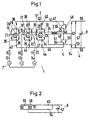
- a three-phase pulse rectifier system 1 is shown, the primary circuit 2 and a secondary circuit 4, which is electrically isolated via a transformer 3 and by combining a subsystem 5 according to the invention Structure with the input part 6 of a prior art Three-phase three-point pulse rectifier system is formed.
- the basic function of the rectifier system 1 consists in the unidirectional conversion of a three-phase input voltage system 7 into a floating DC output voltage 8, in a known manner, series inductors 9, 10, 11 of the Input voltage terminals 12, 13, 14 to the inputs 15, 16, 17 bidirectional, bipolar electronic switching devices 18, 19, 20 are switched, each of which second input terminals 21, 22, 23 with a terminal 24 of the primary winding 25 of the transformer 3 are connected.
- the electronic switching device everyone Phase is achieved, for example, by arranging a unidirectional, unipolar Switch 26 or 27 or 28 above the DC-side terminals 29,30 or 31.32 or 33.34 single-phase diode bridge circuits 35 or 36 or 37 educated.
- the AC-side terminals of these diode bridges correspond the aforementioned inputs of the electronic switching devices 18, 19, 20.
- the subsystem 5 is on the primary side by a collector or on the drain side with the positive primary voltage rail 41 and on the emitter or source side power transistor connected to the second terminal 46 of the primary winding 25 (or generally electronic switch) 47 and an anti-parallel switched diode 48 and through an emitter or source side with the negative primary voltage rail 45 and collector or drain side of the terminal 46 of the primary winding 25 connected power transistor (or generally electronic Switch) 49 and a diode 50 connected in antiparallel to this.
- the secondary winding 51 of the transformer 3 is connected to the input terminals, for example 52 and 53 a single-phase diode bridge 54 with between the output terminals 55 and 56 arranged, the output voltage 8 smoothing capacitance 57 placed so executed in full bridge circuit.
- FIG. 2 An advantageous embodiment variant of the secondary circuit of the invention Device is shown in Fig. 2.
- the secondary winding 51 of the transformer 3 realized by two unilaterally connected winding parts 58 and 59, wherein the connecting terminal 60 of the partial windings has one pole of the output voltage 8 forms.
- the second pole of the output voltage forming node 65 and between 65 and 60 again a smoothing capacitance 57 arranged or a, lower guide losses than realizes a full-bridge circuit center circuit.
- the switching state of the device is determined by the or this subordinate input current control device (e.g. designed as Two-point or tolerance band control) to the control inputs 66,67,68 of the electronic Switching devices 18, 19, 20 of the phase signals are defined.
- the shading part 5 according to the invention is controlled via the control commands 66,67,68 derived to the base and gate terminals 69 and 70 of the Power transistors 47 and 49 applied control signals.
- circuit function one is physically in the input terminal 12 of the switching device flowing and thus positive mains phase current and for the other two phases a physically negative value of Mains current provided that the conditions within an entire network period be recorded, because with a sinusoidal profile of the mains currents (with exception the zero crossings) always two phase currents the same and the third phase current have opposite sign.
- phase switching devices 18, 19, 20 are all switched through, and leaves the rising line phase current flowing through the input terminal 12 the tolerance band is determined by an output assigned to the phase (Advantageously, a sinusoidal profile of the mains current in phase with the associated one Phase voltage ensuring current control device derived Control command 69 of the power transistor 47 switched through and with little time Delay the switching device 18 is opened, whereby the phase current into the Free-wheeling diode 38 commutates and is connected via the primary winding 25 of the transformer 3 and phase switches 19 and 20 closes.
- the current flow in the primary winding 25 leads to the appearance of a corresponding, flow-compensating Current flow in the secondary winding 51 of the transformer 3, which over the Diode bridge 54 into the output voltage 8 or the output capacitor 57 is fed, with which power is supplied to the output circuit and to the secondary winding one physically directed from 52 to 53, into one from 46 to 24 directional primary voltage translated voltage occurs.
- This becomes transformative coupled primary voltage through appropriate gear ratio of the transformer higher than the chained line voltage is selected a reduction of the phase current flowing in via terminal 12 is reached, with which ultimately leave the tolerance band down and the switching device 18 again is switched through, which leads to a renewed increase in the sense of current regulation of the phase current leads.
- phase currents are conducted via the primary winding 25 and thus no counter voltage is coupled into a phase current path, with which one Increase in phase currents and not a decrease in amounts of phase currents would result.
- the output voltage is used indirectly to regulate the mains current used, always according to the number of turns ratio of the transformer transformed sections of the line phase currents fed into the output circuit be, with which even without a detailed study of the function of the invention Device the possibility of regulating the output voltage the amplitude of the mains currents becomes clear. Will the output voltage through electrochemical memory is impressed by the specification of the mains current amplitude the average charging current determines.
- the invention System In addition to the regulation of the mains current and the output voltage is for the invention System also a symmetrical control of the magnetic core ensure. Because a positive or negative current flow through the primary winding always with the occurrence of a positive or negative primary voltage in the simplest case, this can be connected via an equal-share course of the Primary current can be achieved, with which an analogy to the stabilization of the potential of the capacitively formed center of a conventional three-point pulse rectifier system given is.
- the secondary current or detects the secondary voltage of the transformer and the occurrence of a transient DC component can be corrected by regulating the mains current preferred (e.g.
Landscapes
- Engineering & Computer Science (AREA)
- Power Engineering (AREA)
- Rectifiers (AREA)
- Dc-Dc Converters (AREA)
Description
- Fig.1
- Die Grundstruktur (vereinfachte, schematische Darstellung) des Leistungsteiles eines, bei erfindungsgemäßer Verschaltung von Teilsystemen bzw. Bauelementegruppen erfindungsgemäßer Struktur mit Funktionsgruppen eines bekannten unidirektionalen Dreiphasen-Dreipunkt-Pulsgleichrichtersystems resultierenden Gleichrichtersystems mit potentialgetrennter Ausgangsspannung.
- Fig.2
- Eine-Ausführungsvariante des Sekundärkreises der erfindungsgemäßen Vorrichtung.
Claims (3)
- Vorrichtung zur Umformung eines dreiphasigen Spannungssystems (7) in eine frei vorgebbare potentialgetrennte Gleichspannung (8) die einen Primärkreis (2) und einen Sekundärkreis (4) und in jeder Phase des Primärkreises eine, an einen Eingang (15,16,17) einer zugeordneten bidirektionalen, bipolaren elektronischen Schaltvorrichtung (18,19,20) geschaltete Vorschaltinduktivität (9,10,11) aufweist, wobei die jeweils zweiten Eingänge (21,22,23) der Schaltvorrichtungen direkt verbunden sind und eine positive Primärspannungsschiene (41) über Dioden (38,39,40) und eine negative Primärspannungsschiene (45) über Dioden (42,43,44) gespeist wird, dadurch gekennzeichnet, daß ein Wicklungsende (24) der Primärwicklung (25) eines Übertragers (3) mit der, die Eingänge (21,22,23) der Schaltvorrichtungen (18,19,20) verbindenden Leitung und ein kollektor- oder drainseitig an der positiven Primärspannungsschiene (41) liegender Leistungstransistor (47) mit antiparalleler Diode (48) mit der zweiten Klemme (46) der Primärwicklung (25) verschaltet wird und von Wicklungsende (46) abzweigend ein weiterer, emitter- oder sourceseitig mit der negativen Primärspannungsschiene (45) verbundener Leistungstransistor mit antiparalleler Diode (50) angeordnet wird und die Sekundärwicklung (51) des Übertragers (3) in an sich bekannter Weise an die Eingangsklemmen (52) und (53) einer Einphasen-Diodenbrücke (54) mit zwischen den Ausgangsklemmen (55) und (56) angeordneter, die Ausgangsspannung (8) glättender Kapazität (57) gelegt, also in Vollbrückenschaltung ausgeführt wird.
- Vorrichtung nach Anspruch 1, dadurch gekennzeichnet}, daß der Sekundärkreis (4) der Vorrichtung (1) als Mittelpunktsschaltung ausgeführt wird.
- Verfahren zur Steuerung der Vorrichtungen nach Anspruch 1 oder 2 bezugnehmend auf die von einer, der Regelung der Ausgangsspannung (8) unterlagerten Toleranzbandregelung der Netzphasenströme gebildeten Steuersignale, dadurch gekennzeichnet, daß vor dem durch die Stromregelung ausgelösten Abschalten einer positiven Phasenstrom führenden Schaltvorrichtung (18) oder (19) oder (20) der Leistungstransistor (47) durchgeschaltet und erst nach Wiedereinschalten der jeweiligen Schaltvorrichtung wieder abgeschaltet wird und vor Abschalten einer negativen Phasenstrom führenden Schaltvorrichtung (18) oder (19) oder (20) der Leistungstransistor (48) durchgeschaltet und erst nach Wiedereinschalten der jeweiligen Schaltvorrichtung wieder abgeschaltet wird, womit ein kontinuierlicher Verlauf der durch die Eingangsinduktivitäten (9,10,11) eingeprägten Phasenströme sichergestellt und durch die Führung jedenfalls eines Phasenstromes über die Primärwicklung (25) des Übertragers (3) bzw. den dadurch bedingten sekundärseitigen Stromfluß zwischen den Klemmen (24) und (46) die für die Regelung der Netzphasenströme erforderliche, der Netzspannung entgegenwirkende Spannung auftritt, wobei stets jedoch mindestens eine der Phasenschaltvorrichtungen (18) oder (19) oder (20) im durchgeschalteten Zustand verbleibt und die Regelung der Ausgangsspannung in an sich bekannter Weise über die Amplitude der Netzphasenströme erfolgt.
Applications Claiming Priority (3)
| Application Number | Priority Date | Filing Date | Title |
|---|---|---|---|
| AT20797 | 1997-02-10 | ||
| AT0020797A AT406993B (de) | 1997-02-10 | 1997-02-10 | Dreiphasiges pulsgleichrichtersystem mit hochfrequent potentialgetrennter ausgangsspannung |
| PCT/EP1998/000727 WO1998035429A1 (de) | 1997-02-10 | 1998-02-10 | Vorrichtung zur umformung eines dreiphasigen spannungssystems |
Publications (2)
| Publication Number | Publication Date |
|---|---|
| EP0958647A1 EP0958647A1 (de) | 1999-11-24 |
| EP0958647B1 true EP0958647B1 (de) | 2001-07-18 |
Family
ID=3484341
Family Applications (1)
| Application Number | Title | Priority Date | Filing Date |
|---|---|---|---|
| EP98909431A Expired - Lifetime EP0958647B1 (de) | 1997-02-10 | 1998-02-10 | Vorrichtung zur umformung eines dreiphasigen spannungssystems |
Country Status (5)
| Country | Link |
|---|---|
| US (1) | US6061256A (de) |
| EP (1) | EP0958647B1 (de) |
| AT (1) | AT406993B (de) |
| DE (1) | DE59801037D1 (de) |
| WO (1) | WO1998035429A1 (de) |
Families Citing this family (5)
| Publication number | Priority date | Publication date | Assignee | Title |
|---|---|---|---|---|
| AT409569B (de) * | 1999-05-17 | 2002-09-25 | Ascom Energy Systems Ag | Vorrichtung und verfahren zur netzspannungsabhängig thyristorgesteuerten vorladung der ausgangskondensatoren eines dreipunkt-pulsgleichrichtersystems |
| AT500546B1 (de) * | 2001-08-31 | 2009-01-15 | Kolar Johann W | Dreiphasiger hybrid-wechselspannungs- wechselspannungs-direktumrichter minimaler komplexität und hoher kommutierungssicherheit |
| US9219407B2 (en) * | 2006-08-10 | 2015-12-22 | Eaton Industries Company | Cyclo-converter and methods of operation |
| US9728967B2 (en) * | 2014-03-24 | 2017-08-08 | Advanced Fusion Systems Llc | System for improving power factor in an AC power system |
| US10957445B2 (en) | 2017-10-05 | 2021-03-23 | Hill-Rom Services, Inc. | Caregiver and staff information system |
Family Cites Families (4)
| Publication number | Priority date | Publication date | Assignee | Title |
|---|---|---|---|---|
| JPS56163830A (en) * | 1980-05-13 | 1981-12-16 | Inoue Japax Res Inc | Pulse power source |
| JPS5883584A (ja) * | 1981-11-11 | 1983-05-19 | Matsushita Electric Works Ltd | 電源装置 |
| DE3783551T2 (de) * | 1986-10-17 | 1993-07-15 | Toshiba Kawasaki Kk | Leistungsversorgungseinrichtung fuer entladungslast. |
| GB2294165A (en) * | 1994-10-11 | 1996-04-17 | Lumonics Ltd | Power supply for providing a dc supply from a multiphase ac source |
-
1997
- 1997-02-10 AT AT0020797A patent/AT406993B/de not_active IP Right Cessation
-
1998
- 1998-02-10 DE DE59801037T patent/DE59801037D1/de not_active Expired - Lifetime
- 1998-02-10 EP EP98909431A patent/EP0958647B1/de not_active Expired - Lifetime
- 1998-02-10 WO PCT/EP1998/000727 patent/WO1998035429A1/de not_active Ceased
-
1999
- 1999-08-10 US US09/371,448 patent/US6061256A/en not_active Expired - Lifetime
Also Published As
| Publication number | Publication date |
|---|---|
| US6061256A (en) | 2000-05-09 |
| EP0958647A1 (de) | 1999-11-24 |
| AT406993B (de) | 2000-11-27 |
| WO1998035429A1 (de) | 1998-08-13 |
| ATA20797A (de) | 2000-03-15 |
| DE59801037D1 (de) | 2001-08-23 |
Similar Documents
| Publication | Publication Date | Title |
|---|---|---|
| DE112018004721T5 (de) | DC/DC Wandler | |
| DE102009052461A1 (de) | Wechselrichter-Schaltungsanordnung | |
| DE2937995A1 (de) | Brueckenmischschaltung und verfahren zu deren betrieb | |
| EP2026457A1 (de) | Wechselrichter mit zwei Zwischenkreisen | |
| EP0254911B1 (de) | Stromrichterschaltung und Verfahren zu dessen Steuerung | |
| DE102011116593B4 (de) | Wechselrichter mit asymmetrischen Drosseln und einer Steuereinheit zum asymmetrischen Betrieb der Drosseln | |
| DE10153738B4 (de) | Gleichrichterschaltung und Verfahren zu deren Steuerung | |
| EP2026456A1 (de) | Wechselrichter | |
| EP2678933A2 (de) | Verfahren zur erzeugung einer ausgangsspannung an einem modularen mehrstufigem stromrichter und anordnung zur durchführung des verfahrens | |
| EP1245074B1 (de) | Netzrückwirkungsarmes dreiphasen-stromzwischenkreis-pulsgleich-richtersystem mit weitem stellbereich der ausgangsspannung | |
| WO2007003241A1 (de) | Schaltungsanordnung und steuerungsverfahren für einen umrichter | |
| AT406993B (de) | Dreiphasiges pulsgleichrichtersystem mit hochfrequent potentialgetrennter ausgangsspannung | |
| DE3826524A1 (de) | Leistungseinspeiseschaltung mit saugdrossel | |
| DE4026955C2 (de) | Umrichter | |
| WO2019166642A1 (de) | Verfahren zum regeln eines dreiphasen-pulsgleichrichtersystems | |
| CH684510A5 (de) | Durch eine Batterie unterbruchfrei gestütztes Schaltnetzteil. | |
| EP4309277B1 (de) | Verfahren zum betrieb eines gleichstromstellers zur versorgung einer elektrolyseeinrichtung mit elektrischer betriebsenergie und gleichspannungswandler | |
| EP1870996B1 (de) | Schaltung zum Einspeisen elektrischer Energie in ein elektrisches Versorgungsnetz | |
| DE102023200118A1 (de) | Stromrichter und Schaltungsanordnung mit einem solchen Stromrichter | |
| AT500546B1 (de) | Dreiphasiger hybrid-wechselspannungs- wechselspannungs-direktumrichter minimaler komplexität und hoher kommutierungssicherheit | |
| EP3513475A1 (de) | Anlage zum übertragen elektrischer leistung mit filtereinheit | |
| DE102022117740B3 (de) | Verfahren zum Betrieb eines Hybrid-Multilevel-Umrichters, Hybrid-Multilevel-Umrichter und Computerprogramm | |
| DE10138751A1 (de) | Wechselrichter mit schnellschaltenden ansteuerbaren elektronischen Schaltern, insbesondere IGBT-Schaltern, sowie Verfahren zur Ansteuerung eines derartigen Wechselrichters | |
| AT404415B (de) | Weitbereichs-dreiphasen-dreipunkt- pulsgleichrichtersystem | |
| AT408168B (de) | Einstufiges dreiphasen-pulsgleichrichtersystem mit potentialgetrenntem ausgangskreis und eingeprägtem ausgangsstrom |
Legal Events
| Date | Code | Title | Description |
|---|---|---|---|
| PUAI | Public reference made under article 153(3) epc to a published international application that has entered the european phase |
Free format text: ORIGINAL CODE: 0009012 |
|
| 17P | Request for examination filed |
Effective date: 19990216 |
|
| AK | Designated contracting states |
Kind code of ref document: A1 Designated state(s): DE FR GB |
|
| GRAG | Despatch of communication of intention to grant |
Free format text: ORIGINAL CODE: EPIDOS AGRA |
|
| 17Q | First examination report despatched |
Effective date: 20000814 |
|
| GRAG | Despatch of communication of intention to grant |
Free format text: ORIGINAL CODE: EPIDOS AGRA |
|
| GRAH | Despatch of communication of intention to grant a patent |
Free format text: ORIGINAL CODE: EPIDOS IGRA |
|
| RAP1 | Party data changed (applicant data changed or rights of an application transferred) |
Owner name: ASCOM ENERGY SYSTEMS AG |
|
| GRAH | Despatch of communication of intention to grant a patent |
Free format text: ORIGINAL CODE: EPIDOS IGRA |
|
| GRAA | (expected) grant |
Free format text: ORIGINAL CODE: 0009210 |
|
| AK | Designated contracting states |
Kind code of ref document: B1 Designated state(s): DE FR GB |
|
| REF | Corresponds to: |
Ref document number: 59801037 Country of ref document: DE Date of ref document: 20010823 |
|
| GBT | Gb: translation of ep patent filed (gb section 77(6)(a)/1977) |
Effective date: 20011019 |
|
| ET | Fr: translation filed | ||
| REG | Reference to a national code |
Ref country code: GB Ref legal event code: IF02 |
|
| PLBE | No opposition filed within time limit |
Free format text: ORIGINAL CODE: 0009261 |
|
| STAA | Information on the status of an ep patent application or granted ep patent |
Free format text: STATUS: NO OPPOSITION FILED WITHIN TIME LIMIT |
|
| 26N | No opposition filed | ||
| REG | Reference to a national code |
Ref country code: FR Ref legal event code: CD Ref country code: FR Ref legal event code: CA |
|
| REG | Reference to a national code |
Ref country code: GB Ref legal event code: 732E |
|
| REG | Reference to a national code |
Ref country code: FR Ref legal event code: TP |
|
| PGFP | Annual fee paid to national office [announced via postgrant information from national office to epo] |
Ref country code: GB Payment date: 20080118 Year of fee payment: 11 |
|
| PGFP | Annual fee paid to national office [announced via postgrant information from national office to epo] |
Ref country code: FR Payment date: 20080114 Year of fee payment: 11 |
|
| GBPC | Gb: european patent ceased through non-payment of renewal fee |
Effective date: 20090210 |
|
| REG | Reference to a national code |
Ref country code: FR Ref legal event code: ST Effective date: 20091030 |
|
| PG25 | Lapsed in a contracting state [announced via postgrant information from national office to epo] |
Ref country code: GB Free format text: LAPSE BECAUSE OF NON-PAYMENT OF DUE FEES Effective date: 20090210 Ref country code: FR Free format text: LAPSE BECAUSE OF NON-PAYMENT OF DUE FEES Effective date: 20090302 |
|
| PGFP | Annual fee paid to national office [announced via postgrant information from national office to epo] |
Ref country code: DE Payment date: 20170217 Year of fee payment: 20 |
|
| REG | Reference to a national code |
Ref country code: DE Ref legal event code: R071 Ref document number: 59801037 Country of ref document: DE |