EP0941021A1 - Manufacturing process for printed-circuit boards with electrical connection between faces - Google Patents
Manufacturing process for printed-circuit boards with electrical connection between faces Download PDFInfo
- Publication number
- EP0941021A1 EP0941021A1 EP98500066A EP98500066A EP0941021A1 EP 0941021 A1 EP0941021 A1 EP 0941021A1 EP 98500066 A EP98500066 A EP 98500066A EP 98500066 A EP98500066 A EP 98500066A EP 0941021 A1 EP0941021 A1 EP 0941021A1
- Authority
- EP
- European Patent Office
- Prior art keywords
- faces
- circuit
- electrical connection
- printed
- copper
- Prior art date
- Legal status (The legal status is an assumption and is not a legal conclusion. Google has not performed a legal analysis and makes no representation as to the accuracy of the status listed.)
- Withdrawn
Links
Images

Classifications
-
- H—ELECTRICITY
- H05—ELECTRIC TECHNIQUES NOT OTHERWISE PROVIDED FOR
- H05K—PRINTED CIRCUITS; CASINGS OR CONSTRUCTIONAL DETAILS OF ELECTRIC APPARATUS; MANUFACTURE OF ASSEMBLAGES OF ELECTRICAL COMPONENTS
- H05K3/00—Apparatus or processes for manufacturing printed circuits
- H05K3/40—Forming printed elements for providing electric connections to or between printed circuits
- H05K3/42—Plated through-holes or plated via connections
- H05K3/425—Plated through-holes or plated via connections characterised by the sequence of steps for plating the through-holes or via connections in relation to the conductive pattern
- H05K3/428—Plated through-holes or plated via connections characterised by the sequence of steps for plating the through-holes or via connections in relation to the conductive pattern initial plating of through-holes in substrates having a metal pattern
-
- H—ELECTRICITY
- H05—ELECTRIC TECHNIQUES NOT OTHERWISE PROVIDED FOR
- H05K—PRINTED CIRCUITS; CASINGS OR CONSTRUCTIONAL DETAILS OF ELECTRIC APPARATUS; MANUFACTURE OF ASSEMBLAGES OF ELECTRICAL COMPONENTS
- H05K3/00—Apparatus or processes for manufacturing printed circuits
- H05K3/30—Assembling printed circuits with electric components, e.g. with resistor
- H05K3/32—Assembling printed circuits with electric components, e.g. with resistor electrically connecting electric components or wires to printed circuits
- H05K3/34—Assembling printed circuits with electric components, e.g. with resistor electrically connecting electric components or wires to printed circuits by soldering
- H05K3/3457—Solder materials or compositions; Methods of application thereof
- H05K3/3468—Applying molten solder
-
- H—ELECTRICITY
- H05—ELECTRIC TECHNIQUES NOT OTHERWISE PROVIDED FOR
- H05K—PRINTED CIRCUITS; CASINGS OR CONSTRUCTIONAL DETAILS OF ELECTRIC APPARATUS; MANUFACTURE OF ASSEMBLAGES OF ELECTRICAL COMPONENTS
- H05K2201/00—Indexing scheme relating to printed circuits covered by H05K1/00
- H05K2201/09—Shape and layout
- H05K2201/09209—Shape and layout details of conductors
- H05K2201/095—Conductive through-holes or vias
- H05K2201/09572—Solder filled plated through-hole in the final product
-
- H—ELECTRICITY
- H05—ELECTRIC TECHNIQUES NOT OTHERWISE PROVIDED FOR
- H05K—PRINTED CIRCUITS; CASINGS OR CONSTRUCTIONAL DETAILS OF ELECTRIC APPARATUS; MANUFACTURE OF ASSEMBLAGES OF ELECTRICAL COMPONENTS
- H05K2203/00—Indexing scheme relating to apparatus or processes for manufacturing printed circuits covered by H05K3/00
- H05K2203/04—Soldering or other types of metallurgic bonding
- H05K2203/044—Solder dip coating, i.e. coating printed conductors, e.g. pads by dipping in molten solder or by wave soldering
-
- H—ELECTRICITY
- H05—ELECTRIC TECHNIQUES NOT OTHERWISE PROVIDED FOR
- H05K—PRINTED CIRCUITS; CASINGS OR CONSTRUCTIONAL DETAILS OF ELECTRIC APPARATUS; MANUFACTURE OF ASSEMBLAGES OF ELECTRICAL COMPONENTS
- H05K3/00—Apparatus or processes for manufacturing printed circuits
- H05K3/30—Assembling printed circuits with electric components, e.g. with resistor
- H05K3/32—Assembling printed circuits with electric components, e.g. with resistor electrically connecting electric components or wires to printed circuits
- H05K3/34—Assembling printed circuits with electric components, e.g. with resistor electrically connecting electric components or wires to printed circuits by soldering
- H05K3/3452—Solder masks
Definitions
- the present invention refers to a new manufacturing process for printed-circuit boards, especially boards with electrical connections between faces, that supposes a notable simplification and a subsequent reduction in cost compared to conventional processes.
- the process is ideally suited for the type of printed-circuit boards used in the automobile industry and for electronic consumer goods such as video, hi-fi, television and telephony.
- the base materials used to obtain boards are fibreglass- and epoxy resin-based "FR-4" and "CEM-1", which is a material composed of Fiberglas, paper and epoxy resin.
- This type of board would first be metallized, then punched, metallized again and finally etched, leading to the elimination of the two copper layers in order to define the tracks.
- the process proposed by the invention resolves the aforementioned repercussions in a highly satisfactory way, considering that it renders bore holes useful for inserting components, leading to the reduction in size of the printed circuit in addition to a substantial improvement in the electrical characteristics of the printed circuit compared to the classic surfacing of the holes with "silver ink”.
- Metallization is also performed on laminates that cost less than the FR-4, avoiding the typical problems that traditional copper metallization has on these laminates.
- the process proposed by the invention enables bore holes to be used by chemically making a metallic deposit. This is to say, without electrolyte processes on one or more of the holes of the printed circuit, depending on its needs.
- This process can be applied to the majority of base materials available on the market, and, in particular, to the following types: CEM-3, CEM-1, FR-2 and FR-1.
- the manufacturing process begins with the preparation of the base material by means of wet-process polishing, leaving the copper in perfect condition for a second phase, silk-screening, in which the copper pattern of the circuit is impressed and the excess copper is eliminated by means of chemical etching.
- impression is performed with inks resistant to the chemical processes of metallization that will connect the two faces of the circuit, in addition to its punching.
- soldering mask is applied, along with identifying inks and other conductive inks.
- a soldering jet then ensures that the metallized bore holes are completely filled with tin/lead.
- the unit is punched, obtaining the bore holes (5) that are, in their number and positioning, suitable for the electrical connection between the two faces of the board as well as for the insertion of electronic components of the circuit.
- the unit again undergoes an impression with inks (6) resistant to the chemical processes of metallization in order to leave the areas (7) meant to connect the two faces of the circuit through the bore holes (5) clear.
- the chemical metallization phase is then carried out, and, as it has been stated previously, it is performed with a nickel-phosphorous alloy (8), as seen in Figure 7.
- This chemical metallization (8) affects only those bore holes (5) where the connection between the two faces of the board is going to be carried out, while the normal holes (9) will not be affected by this metallizing.
- identifying inks and other conductive inks (10) are applied in order to improve adhesion so that the soldering mask represented in Figure 8 enables, after the soldering jet phase (shown in Figure 9), the metallized bore holes (5) to be completely filled with a tin/lead mass (11), while in the normal holes (9) the soldering mass (12) can be applied to only one of their openings, as is shown in Figure 9.
Landscapes
- Engineering & Computer Science (AREA)
- Manufacturing & Machinery (AREA)
- Microelectronics & Electronic Packaging (AREA)
- Printing Elements For Providing Electric Connections Between Printed Circuits (AREA)
Abstract
Starting from the base material of a board (1) that has each of its
two faces surfaced with copper coating (2), the circuit is defined by
means of the partial elimination of the copper by chemical etching.
Following this, the punching of the unit is undertaken in order to
obtain the bore holes (5) through which the electrical connection
between the two faces of the circuit will be preformed. This connection
is performed by means of a chemical metallizing in which a metal layer
(8) from a nickel-phosphorous base alloy is applied to the holes (5) and
to the area surrounding them, leaving the board, after the application
of a solder mask, identification ink and conductive inks, in a condition
to pass under the soldering jet, which will fill the metallized bore
holes (5) with a tin/lead mass.
Description
The present invention refers to a new manufacturing process for
printed-circuit boards, especially boards with electrical connections between
faces, that supposes a notable simplification and a subsequent reduction in
cost compared to conventional processes.
The process is ideally suited for the type of printed-circuit boards used
in the automobile industry and for electronic consumer goods such as video,
hi-fi, television and telephony.
In the invention's preferred sphere of practical application, the base
materials used to obtain boards are fibreglass- and epoxy resin-based "FR-4"
and "CEM-1", which is a material composed of Fiberglas, paper and epoxy
resin.
This type of board, according to conventional techniques, would first
be metallized, then punched, metallized again and finally etched, leading to
the elimination of the two copper layers in order to define the tracks.
This solution has its own problematic repercussions that centre on the
following aspects:
- Part of the hole remains unused.
- Poor characteristics of electrical conductivity are obtained.
- Metallization is performed on expensive laminates.
- The process involves an extremely long period of application.
- Highly contaminating electrolyte baths are used.
The process proposed by the invention resolves the aforementioned
repercussions in a highly satisfactory way, considering that it renders bore
holes useful for inserting components, leading to the reduction in size of the
printed circuit in addition to a substantial improvement in the electrical
characteristics of the printed circuit compared to the classic surfacing of the
holes with "silver ink". Metallization is also performed on laminates that cost
less than the FR-4, avoiding the typical problems that traditional copper
metallization has on these laminates.
More concretely, the process proposed by the invention enables bore
holes to be used by chemically making a metallic deposit. This is to say,
without electrolyte processes on one or more of the holes of the printed
circuit, depending on its needs.
This process can be applied to the majority of base materials available
on the market, and, in particular, to the following types: CEM-3, CEM-1, FR-2
and FR-1.
In order to obtain this metallization, silk-screen impressions are all that
are used. This supposes a series of advantages that centre on the following
aspects:
- Greater format size of the circuit board, which translates into an increase in productivity.
- Reduced cost in the tool rigs used.
- Improvements of the electrical benefits of the bore hole.
- Better resistance to climatic and thermal shock tests.
The manufacturing process begins with the preparation of the base
material by means of wet-process polishing, leaving the copper in perfect
condition for a second phase, silk-screening, in which the copper pattern of
the circuit is impressed and the excess copper is eliminated by means of
chemical etching.
More specifically, prior to the preparation of the copper surface,
impression is performed with inks resistant to the chemical processes of
metallization that will connect the two faces of the circuit, in addition to its
punching.
Following this, chemical metallization is performed on those holes that
will connect the two faces of the circuit, having planned―with this constituting
one of the essential characteristics of the invention―that this metallization is
performed with a nickel-phosphorous alloy in which the phosphorous is used
in a proportion that ranges between 11% and 13%.
Lastly, a soldering mask is applied, along with identifying inks and
other conductive inks. A soldering jet then ensures that the metallized bore
holes are completely filled with tin/lead.
In order to complement the present description and with the aim of
helping to better understand the characteristics of the invention, as per a
preferred example of its practical performance, a set of drawings, of an
illustrative, non-restrictive nature, is used to represent the following:
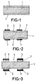
In Figure 1, it can be seen how the process begins with the base
material of a board (1) that has its faces equally covered by copper (2).
Following this, by applying a resistant etching ink (3), the copper areas (4)
needed to define the circuit are eliminated, as it can be seen in Figure 3.
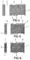
Following this, the unit is punched, obtaining the bore holes (5) that
are, in their number and positioning, suitable for the electrical connection
between the two faces of the board as well as for the insertion of electronic
components of the circuit.
The unit again undergoes an impression with inks (6) resistant to the
chemical processes of metallization in order to leave the areas (7) meant to
connect the two faces of the circuit through the bore holes (5) clear.
The chemical metallization phase is then carried out, and, as it has
been stated previously, it is performed with a nickel-phosphorous alloy (8), as
seen in Figure 7. This chemical metallization (8) affects only those bore holes
(5) where the connection between the two faces of the board is going to be
carried out, while the normal holes (9) will not be affected by this metallizing.
Following this, and after the copper surface (2) has been suitably
prepared, identifying inks and other conductive inks (10) are applied in order
to improve adhesion so that the soldering mask represented in Figure 8
enables, after the soldering jet phase (shown in Figure 9), the metallized bore
holes (5) to be completely filled with a tin/lead mass (11), while in the normal
holes (9) the soldering mass (12) can be applied to only one of their
openings, as is shown in Figure 9.
It is felt that a more detailed description is not required for any expert in
the field to recognise the scope of the invention and the advantages that are
to be derived from it.
The materials, form, size and disposition of the elements will be
susceptible to variation so long as it does not suppose an alteration in the
essence of the invention.
The terms that have been used to write up this report should always be
taken in their broadest, non-restrictive sense.
Claims (3)
- Manufacturing process for printed-circuit boards with electrical connection between faces, characterised by the following operational phases:Preparation of base material by means of wet-process polishing in order to leave the copper in a condition for impression.Resistant impression, by means of silk-screening, of the copper pattern of the circuit.Elimination of the excess copper by means of chemical etching in order to define the circuit.Punching of the material in order to finish the circuit, using the bore holes for the electrical connection between the faces of the circuit.Impression with inks resistant to the chemical processes of metallization that will connect the two faces of the circuit.Chemical metallization for the electrical connection between faces as well as for the insertion of components.Preparation of the copper surface for adherence to the soldering mask and to identifying and conductive inks.Passage under the soldering jet to fill the metallized bore holes with tin/lead.
- Manufacturing process for printed-circuit boards with electrical connection between faces, as per Claim #1, characterised by the chemical metallization phase that is performed with a nickel-phosphorous alloy.
- Manufacturing process for printed-circuit boards with electrical connection between faces, as per Claim #2, characterised by the aforementioned nickel-phosphorous alloy, in which the proportion of phosphorous accounts for between 11% and 13%.
Priority Applications (1)
| Application Number | Priority Date | Filing Date | Title |
|---|---|---|---|
| EP98500066A EP0941021A1 (en) | 1998-03-06 | 1998-03-06 | Manufacturing process for printed-circuit boards with electrical connection between faces |
Applications Claiming Priority (1)
| Application Number | Priority Date | Filing Date | Title |
|---|---|---|---|
| EP98500066A EP0941021A1 (en) | 1998-03-06 | 1998-03-06 | Manufacturing process for printed-circuit boards with electrical connection between faces |
Publications (1)
| Publication Number | Publication Date |
|---|---|
| EP0941021A1 true EP0941021A1 (en) | 1999-09-08 |
Family
ID=8235808
Family Applications (1)
| Application Number | Title | Priority Date | Filing Date |
|---|---|---|---|
| EP98500066A Withdrawn EP0941021A1 (en) | 1998-03-06 | 1998-03-06 | Manufacturing process for printed-circuit boards with electrical connection between faces |
Country Status (1)
| Country | Link |
|---|---|
| EP (1) | EP0941021A1 (en) |
Cited By (1)
| Publication number | Priority date | Publication date | Assignee | Title |
|---|---|---|---|---|
| CN109769344A (en) * | 2017-11-10 | 2019-05-17 | 鹏鼎控股(深圳)股份有限公司 | The manufacturing method of circuit board and the circuit board |
Citations (5)
| Publication number | Priority date | Publication date | Assignee | Title |
|---|---|---|---|---|
| GB1223939A (en) * | 1968-08-26 | 1971-03-03 | Marconi Co Ltd | Improvements in or relating to printed circuits |
| JPH01120852A (en) * | 1987-11-04 | 1989-05-12 | Hitachi Chem Co Ltd | Plastic chip carrier |
| JPH07106718A (en) * | 1993-10-06 | 1995-04-21 | Nippon Avionics Co Ltd | Printed circuit board with heat sink |
| GB2284509A (en) * | 1993-12-03 | 1995-06-07 | John Frederick David Knopp | Method of making a printed circuit board |
| EP0762813A1 (en) * | 1995-08-25 | 1997-03-12 | Macdermid Incorporated | Method for the manufacture of printed circuit boards |
-
1998
- 1998-03-06 EP EP98500066A patent/EP0941021A1/en not_active Withdrawn
Patent Citations (5)
| Publication number | Priority date | Publication date | Assignee | Title |
|---|---|---|---|---|
| GB1223939A (en) * | 1968-08-26 | 1971-03-03 | Marconi Co Ltd | Improvements in or relating to printed circuits |
| JPH01120852A (en) * | 1987-11-04 | 1989-05-12 | Hitachi Chem Co Ltd | Plastic chip carrier |
| JPH07106718A (en) * | 1993-10-06 | 1995-04-21 | Nippon Avionics Co Ltd | Printed circuit board with heat sink |
| GB2284509A (en) * | 1993-12-03 | 1995-06-07 | John Frederick David Knopp | Method of making a printed circuit board |
| EP0762813A1 (en) * | 1995-08-25 | 1997-03-12 | Macdermid Incorporated | Method for the manufacture of printed circuit boards |
Non-Patent Citations (2)
| Title |
|---|
| PATENT ABSTRACTS OF JAPAN vol. 13, no. 364 (E - 805) 14 August 1989 (1989-08-14) * |
| PATENT ABSTRACTS OF JAPAN vol. 95, no. 7 31 August 1995 (1995-08-31) * |
Cited By (2)
| Publication number | Priority date | Publication date | Assignee | Title |
|---|---|---|---|---|
| CN109769344A (en) * | 2017-11-10 | 2019-05-17 | 鹏鼎控股(深圳)股份有限公司 | The manufacturing method of circuit board and the circuit board |
| CN109769344B (en) * | 2017-11-10 | 2021-07-20 | 鹏鼎控股(深圳)股份有限公司 | Circuit board and manufacturing method thereof |
Similar Documents
| Publication | Publication Date | Title |
|---|---|---|
| DE3125518C2 (en) | Method of making a thin wiring assembly - US Pat | |
| US4622106A (en) | Methods for producing printed circuits | |
| EP0127955B1 (en) | Manufacture of printed circuit boards | |
| US7240431B2 (en) | Method for producing multilayer printed wiring board, multilayer printed wiring board, and electronic device | |
| EP0941021A1 (en) | Manufacturing process for printed-circuit boards with electrical connection between faces | |
| GB2247361A (en) | Conductive through-holes in printed wiring boards | |
| KR900005308B1 (en) | Printed circuit board method | |
| US6165595A (en) | Component mounting board, process for producing the board, and process for producing the module | |
| RU2149525C1 (en) | Process of manufacture of printed circuit board | |
| US20050062587A1 (en) | Method and structure of a substrate with built-in via hole resistors | |
| JPH0265194A (en) | Manufacture of printed wiring board with thick film element | |
| JPS584999A (en) | Method of producing printed circuit board | |
| JP3324114B2 (en) | Printed board | |
| JP2603863B2 (en) | Printed wiring board | |
| WO2000046837B1 (en) | Improved circuit board manufacturing process | |
| KR930005352B1 (en) | Plating method of printed circuit board | |
| JPS5877287A (en) | Method of producing printed circuit board | |
| JPS5818796B2 (en) | Manufacturing method for printed wiring boards | |
| JPS62150896A (en) | Formation of wiring on wiring circuit board | |
| JPH09181453A (en) | Multilayer wiring board and its manufacturing method | |
| JPS5841799B2 (en) | printed wiring board | |
| CN112218429A (en) | Circuit board preparation method and circuit board | |
| JPS60239093A (en) | Method of producing printed circuit board | |
| JPH02148793A (en) | Manufacture of printed wiring board | |
| JPS60187093A (en) | Metal printed board and method of producing same |
Legal Events
| Date | Code | Title | Description |
|---|---|---|---|
| PUAI | Public reference made under article 153(3) epc to a published international application that has entered the european phase |
Free format text: ORIGINAL CODE: 0009012 |
|
| AK | Designated contracting states |
Kind code of ref document: A1 Designated state(s): BE DE FR GB IT PT |
|
| AX | Request for extension of the european patent |
Free format text: AL;LT;LV;MK;RO;SI |
|
| AKX | Designation fees paid |
Free format text: BE DE FR GB IT PT |
|
| 17P | Request for examination filed |
Effective date: 20000303 |
|
| 17Q | First examination report despatched |
Effective date: 20030715 |
|
| STAA | Information on the status of an ep patent application or granted ep patent |
Free format text: STATUS: THE APPLICATION IS DEEMED TO BE WITHDRAWN |
|
| 18D | Application deemed to be withdrawn |
Effective date: 20040127 |