EP0939490A2 - Koinzidenzdetektorschaltung - Google Patents
Koinzidenzdetektorschaltung Download PDFInfo
- Publication number
- EP0939490A2 EP0939490A2 EP99102710A EP99102710A EP0939490A2 EP 0939490 A2 EP0939490 A2 EP 0939490A2 EP 99102710 A EP99102710 A EP 99102710A EP 99102710 A EP99102710 A EP 99102710A EP 0939490 A2 EP0939490 A2 EP 0939490A2
- Authority
- EP
- European Patent Office
- Prior art keywords
- comparator
- circuit
- control signal
- signal
- output
- Prior art date
- Legal status (The legal status is an assumption and is not a legal conclusion. Google has not performed a legal analysis and makes no representation as to the accuracy of the status listed.)
- Withdrawn
Links
Images



Classifications
-
- H—ELECTRICITY
- H03—ELECTRONIC CIRCUITRY
- H03K—PULSE TECHNIQUE
- H03K19/00—Logic circuits, i.e. having at least two inputs acting on one output; Inverting circuits
- H03K19/20—Logic circuits, i.e. having at least two inputs acting on one output; Inverting circuits characterised by logic function, e.g. AND, OR, NOR, NOT circuits
- H03K19/21—EXCLUSIVE-OR circuits, i.e. giving output if input signal exists at only one input; COINCIDENCE circuits, i.e. giving output only if all input signals are identical
- H03K19/215—EXCLUSIVE-OR circuits, i.e. giving output if input signal exists at only one input; COINCIDENCE circuits, i.e. giving output only if all input signals are identical using field-effect transistors
-
- G—PHYSICS
- G06—COMPUTING OR CALCULATING; COUNTING
- G06F—ELECTRIC DIGITAL DATA PROCESSING
- G06F7/00—Methods or arrangements for processing data by operating upon the order or content of the data handled
- G06F7/02—Comparing digital values
Definitions
- the present invention generally relates to a comparator, and, more particularly, to speed improvements in a bit data comparator.
- Comparators have many uses in electronic devices. For example, in order to check an access address to a memory device, a comparator for comparing two address data signals is used.
- the comparator includes XOR circuits and a logic circuit connected to the XOR circuits. Each XOR circuit detects the coincidence of each data bit. When the two bits coincide, a signal having a logical value of "0" (L level) is output, and when the two bits do not coincide, a signal having a logical value of "1" (H level) is output.
- the logic circuit receives the output signals from the XOR circuits and determines the coincidence of the two address signals based on whether the logical value of each signal is 0.
- the logic circuit may be, for example, an n-input NAND circuit.
- the n-input NAND circuit includes a number n of pMOS transistors connected in parallel to a power supply and a number n of nMOS transistors connected in series between the pMOS transistors and ground.
- the output signal of the NAND circuit is obtained from the node between the pMOS transistors and the uppermost stage nMOS transistor.
- the next stage nMOS transistor turns on only when the nMOS transistor near the power supply turns on. Accordingly, the operating speed of the NAND circuit is quite slow.
- FIG. 1 is a block diagram of a conventional comparator 10.
- the comparator 10 compares two 12-bit data words A11 to A0 and B11 to B0.
- the comparator 10 includes twelve XOR circuits 11A to 11L (only eight XOR circuits are illustrated), three 4-input NOR circuits 12A to 12C (only two NOR circuits are illustrated), one 4-input NAND circuit 13, and an inverter 14.
- the XOR circuits 11A to 11L receive the data bits A0 to A11 and the data bits B0 to B11, respectively. When two compared bits coincide, a signal having the logical L level is output, and when the two bits do not coincide, a signal having the logical H level is output.
- the 4-input NOR circuit 12A receives the output signals from the XOR circuits 11A to 11D.
- the 4-input NOR circuit 12B receives the output signals from the XOR circuits 11E to 11H.
- the 4-input NOR circuit 12C receives the output signals from the XOR circuits 11I to 11L.
- Each of the 4-input NOR circuits 12A to 12C outputs a signal having the logical L level when any one of the four input signals has the logical H level.
- the 4-input NAND circuit 13 receives the output signals from the three 4-input NOR circuits 12A to 12C and outputs an output signal in accordance with a control signal CS. For example, when the control signal CS has the logical H level and all of the output signals from the 4-input NOR circuits 12A to 12C have the logical H levels, the NAND circuit 13 outputs an output signal having the logical L level and the inverter 14 outputs an output signal OUT having the logical H level. In other words, when the two data words coincide and the control signal is high, the NAND circuit 13 outputs a signal having the logical L level.
- the comparator 10 has a 2-stage configuration, it does not operate at a very high speed. In particular, as the number of data bits increases, the circuit configuration exceeds 2-stages, so that the operating speed becomes even slower.
- the NOR circuit includes n number of pMOS transistors connected in series to the power supply and n number of nMOS transistors connected in parallel between the pMOS transistors and a ground. Accordingly, as the number of the input signal increases, for example by one, an additional pMOS transistor and an additional nMOS transistor become necessary. As a result, the number of elements increases and the circuit area increases.
- a comparator in one aspect of the present invention, includes a plurality of coincidence detection circuits for comparing first bit data and second bit data and generating a plurality of detection signals that indicate a coincidence detection result for each bit.
- a decision circuit receives the plurality of detection signals and generates a decision signal indicating the coincidence decision results of the first and second bit data.
- the decision circuit includes a plurality of switching circuits that operate in parallel in response to the plurality of detection signals, respectively, to generate the decision signal.
- a comparator in another aspect of the present invention, includes a plurality of coincidence detection circuits for comparing first bit data and second bit data and generating a plurality of detection signals that indicate a coincidence detection result for each bit.
- a first inverter circuit receives a first control signal and outputs an inverse signal of the first control signal from an output terminal thereof.
- a plurality of switching circuits are connected in parallel between the output terminal of the first inverter circuit and ground and receives the plurality of detection signals and generates a decision output signal.
- a comparator that compares a first data word with a second data word.
- the comparator includes a plurality of two input XOR gates. Each of the XOR gates receives one bit of the first word and a corresponding bit of the second word and outputs a coincidence detection signal.
- a first inverter circuit receives a control signal and generates an inverted control signal.
- a decision circuit receives the inverted control signal from the first inverter circuit and receives each of the coincidence detection signals from the plurality of XOR gates, and generates a decision circuit output signal.
- the decision circuit includes a second inverter circuit has an input terminal connected to the output of the first inverter circuit and receives the inverted control signal, and an output terminal.
- the output terminal forms a first node.
- a plurality of transistors are connected in parallel between the first node and ground. The gates of the transistors receive the respective coincidence detection signals.
- a two input NAND gate receives the decision circuit output signal and the control signal and generates a comparator output signal.
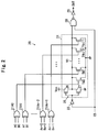
- FIG. 2 is a block circuit diagram of a comparator 20 according to a first embodiment of the present invention.
- the comparator 20 is preferably installed in a device, such as a solid-state video camera, and determines the coincidence of two digital data, such as address signals, to check the address whenever accessing a memory.
- the comparator 20 compares n-bit data An-1 to A0 and n-bit data Bn-1 to B0.
- the comparator 20 includes a number n of XOR circuits 21A0 to 21An-1 as coincidence detection circuits (only four XOR circuits are illustrated), an inverter 23, a dynamic NOR circuit 24 as a decision circuit, a 2-input NAND circuit 28, and an output inverter 29.
- the XOR circuits 21A0 to 21An-1 are preferably 2 input XOR circuits which receive bits A0 to An-1 and bits B0 to Bn-1, respectively. When the two bits compared by the XOR gate coincide, a signal having the logical L level is output. When the two bits do not coincide, a signal having the logical H level is output.
- the inverter 23 receives a control signal CS (see FIG. 3) in which the logical level is alternately inverted at a predetermined cycle.
- the inverter 23 supplies an inverse of the control signal CS to the dynamic NOR circuit 24. For example, when the control signal CS has the logical H level, the inverter 23 supplies a signal having the logical L level to the dynamic NOR circuit 24.
- the dynamic NOR circuit 24 includes an inverter 25 and a number n of nMOS transistors TN0 to TNn-1 as switching circuits.
- the inverter 25 has an input terminal for receiving the output signal of the inverter 23 and an output terminal (node N1) for outputting the inverse signal.
- the inverter 25 includes a pMOS transistor 26 and an nMOS transistor 27 connected in series between a high potential power supply Vcc and ground. It is preferable that the pMOS transistor 26 has a large "on" resistance.
- the inverter 25, for example, reverses the output signal having the logical L level from the inverter 23 and outputs the inverse signal (control signal CS) having the logical H level.
- the nMOS transistors TN0 to TNn-1 are connected in parallel between the node N1 and ground.
- the output signals from the XOR circuits 21A0 to 21An-1 are applied to the gates of the nMOS transistors TN0 to TNn-1, respectively.
- the respective nMOS transistors TN0 to TNn-1 turn on when the output signals of the corresponding XOR circuits 21A0 to 21An-1 have the logical H levels, and the node N1 is set to the logical L level. In other words, when any one of the output signals of the XOR circuits 21A0 to 21An-1 has the logical H level, the node N1 is set to the logical L level.
- the 2-input NAND circuit 28 receives the control signal CS and the voltage signal of the node N1 (the output signal of the dynamic NOR circuit 24) and outputs the output signal in accordance with the control signal CS.
- An output inverter 29 is connected to the output of the NAND circuit 28 and receives the NAND circuit 28 output at its input terminal. For example, when the control signal CS has the logical H level and the output signal of the dynamic NOR circuit 24 has the logical H level, the NAND circuit 28 outputs a signal having the logical L level and the output inverter 29 outputs a output signal OUT having the logical H level. In other words, when the two data words A and B coincide, the NAND circuit 28 outputs a signal having the logical L level.
- data word refers to multiple bits of data, but not to any specific word length or number of bits.
- the logical L level of the control signal CS is switched to the logical H level and data B is applied to the XOR circuits 21A0 to 21An-1.
- the inverter 23 supplies a signal having the logical L level to the inverter 25, and the pMOS transistor 26 of the inverter 25 turns on.
- bit data A is not input, although bit data B is input, the logical levels of the output signals of the XOR circuits 21A0 to 21An-1 are indefinite.
- the logical level of the node N1 is indefinite.
- the logical level of the output signal OUT is indefinite as shown in FIG. 3 by oblique lines.
- the respective XOR circuits 21A0 to 21An-1 determine whether the corresponding bits A0, B0, A1, B1, ... coincide, respectively, and output decision result signals.
- all of the XOR circuits 21A0 to 21An-1 output signals having the logical L level.
- all of the nMOS transistors TN0 to TNn-1 of the dynamic NOR circuit 24 turn off, and the node N1 is set to the logical H level by the pMOS transistor 26 being turned on.
- the NAND circuit 28 receives the control signal CS and the output signal of the dynamic NOR circuit 24, in which each has the logical H level, and supplies an output signal having the logical L level to the output inverter 29.
- the inverter 29 then outputs an output signal OUT having the logical H level.
- the XOR circuit that corresponds to the bit outputs an output signal having the logical H level and the other XOR circuits output signals having the logical L level.
- the corresponding one nMOS transistor of the dynamic NOR circuit 24 turns on in response to the XOR output signal having the logical H level.
- the nMOS transistor TN0 turns on in response to the output signal of the XOR circuit 21A0 having the logical H level.
- the voltage of the power supply Vcc is divided by the resistance of the pMOS transistor 26 being turned on and the resistance of the nMOS transistor TN0 being turned on. At this time, since the "on" resistance of the nMOS transistor 26 is relatively large, the node N1 is set to the logical L level.
- the NAND circuit 28 receives the control CS having the logical H level and the output signal of the dynamic NOR circuit 24 having the logical L level and supplies an output signal having the logical H level to the output inverter 29.
- the output inverter 29 outputs an output signal OUT low indicating that data A and B do not coincide.
- the comparator 20 includes the dynamic NOR circuit 24 having a number n of nMOS transistors TN0 to TNn-1 connected in parallel to the output terminal (node N1) of the inverter 25.
- the respective nMOS transistors TN0 to TNn-1 operate in response to the output signals of the respective XOR circuits 21A0 to 21An-1.
- the nMOS transistors TN0 to TNn-1 operate in parallel. Accordingly, the comparator 20 operates at high speed.
- the NAND gate 28 remains a 2 input NAND gate, and thus not increase in size.
- FIG. 4 is a circuit diagram of a comparator 30 according to a second embodiment of the present invention.
- the comparator 30 includes a number n of XOR ⁇ XNOR circuits 31A0 to 31An-1 (only four are illustrated), the inverter 23, the dynamic NOR circuit 24, the 2-input NAND circuit 28, the output inverter 29, and a voltage supply circuit 32.
- the XOR ⁇ XNOR circuits 31A0 to 31An-1 receive the bits A0 to An-1 and the bits B0 to Bn-1, respectively. When the two bits coincide, a signal having the logical H level is output from an XNOR output terminal (marked with a circle), and a signal having the logical L level is output from an XOR output terminal (not marked). The XOR ⁇ XNOR circuits 31A0 to 31An-1 further output a signal having the logical L level from the XNOR output terminal and output a signal having the logical H level from the XOR output terminal when the two bits do not coincide.
- the voltage supply circuit 32 includes an inverter 33, pMOS transistors TP0 to TPn-1, and a PMOS transistor 37.
- the inverter 33 has an input terminal for receiving the control signal CS and an output terminal (node N2) for outputting an inverse signal of the control signal CS.
- the inverter 33 includes a pMOS transistor 34 and an nMOS transistor 35 connected in series between a high potential power supply Vcc and ground. It is preferable that the nMOS transistor 35 has a large "on" resistance.
- the inverter 33 for example, inverts the control signal CS having the logical H level and outputs an inverse signal having the logical L level.
- the pMOS transistors TP0 to TPn-1 are connected in parallel between the node N2 and the high potential power supply Vcc.
- the output signals from the respective XNOR circuits 31A0 to 31An-1 are applied to the gates of the respective pMOS transistors TP0 to TPn-1, respectively.
- the respective pMOS transistors TP0 to TPn-1 turn on when the output signals of the corresponding XNOR circuits 31A0 to 31An-1 have the logical L levels, and the node N2 is set to the logical H level. In other words, when any one of the output signals of the XNOR circuits 31A0 to 31An-1 has the logical L level, the node N2 is set to the logical H level.
- the pMOS transistor 37 is connected between the high potential power supply Vcc and the node N1 and has a gate connected to the node N2.
- the pMOS transistor 37 turns on when the node N2 has the logical L level and supplies a high potential to the node N1.
- the control signal CS and data B are applied to the comparator 30 prior to data A.
- the logical L level of the control signal CS is switched to the logical H level.
- the inverter 23 supplies a signal having the logical L level to the inverter 25, and the pMOS transistor 26 of the inverter 25 turns on.
- the logical levels of the output signals of the XOR ⁇ XNOR circuits 31A0 to 31An-1 are indefinite. Accordingly, the logical levels of the node N1 and the output signal OUT are indefinite.
- the nMOS transistor 35 of the inverter 33 turns on in response to the control signal CS having the logical H level. Nevertheless, the logical levels of the output signals of the XOR ⁇ XNOR circuits 31A0 to 31An-1 are indefinite. Accordingly, the logical level of the node N2 is indefinite.
- the respective XOR ⁇ XNOR circuits 31A0 to 31An-1 determine whether the corresponding bits A0, B0, A1, B1, ... coincide, and output decision result signals.
- all of the XOR ⁇ XNOR circuits 31A0 to 31An-1 output signals having the logical L level from the XOR output terminals and output signals having the logical H level from the XNOR output terminals.
- all of the nMOS transistors TN0 to TNn-1 of the dynamic NOR circuit 24 turn off, and the node N1 is set to the logical H level by the pMOS transistor 26 being turned on.
- the NAND circuit 28 receives the control signal CS and the output signal of the dynamic NOR circuit 24 in which each has the logical H level, and supplies the output signal having the logical L level to the output inverter 29.
- the inverter 29 then outputs an output signal OUT having the logical H level.
- the nMOS transistor TN0 turns on in response to the output signal of the XOR ⁇ XNOR circuit 31A having the logical H level
- the pMOS transistor TP0 turns on in response to the signal from the XNOR output terminal of the XOR ⁇ XNOR circuit 31A0 having the logical L level.
- the voltage of the power supply Vcc is divided by the on resistance of the pMOS transistor 26 being turned on and the on resistance of the nMOS transistor TP0 being turned on.
- the voltage of the power supply Vcc is divided by the on resistance of the nMOS transistor 35 being turned on and the on resistance of the pMOS transistor TP0 being turned on.
- the node N2 is set to the logical H level and the pMOS transistor 37 turns off.
- the NAND circuit 28 receives the control signal CS having the logical H level and the output signal of the dynamic NOR circuit 24 having the logical L level and supplies an output signal having the logical H level to the output inverter 29.
- the output inverter 29 indicates that data A and B do not coincide and outputs the output signal OUT having the logical L level.
- the comparator 30 includes the voltage supply circuit 32 that supplies the voltage of the power supply Vcc to the node N1 when data A and B coincide. Accordingly, the node N1 is quickly set to the logical H level, and the comparator 30 operates at high speed.
- the inverter 23 may be omitted.
- the inverse signal of the control signal CS is provided to the dynamic NOR circuit 24.
- the NAND circuit 28 is changed to suit the inverse signal.
- the comparators 20 and 30 may be formed using FETs (field-effect transistors) instead of MOS transistors.
- the data A and B may be supplied simultaneously to the comparators 20 and 30.
Landscapes
- Physics & Mathematics (AREA)
- Engineering & Computer Science (AREA)
- Theoretical Computer Science (AREA)
- General Physics & Mathematics (AREA)
- General Engineering & Computer Science (AREA)
- Computational Mathematics (AREA)
- Mathematical Physics (AREA)
- Computing Systems (AREA)
- Mathematical Analysis (AREA)
- Mathematical Optimization (AREA)
- Pure & Applied Mathematics (AREA)
- Computer Hardware Design (AREA)
- Logic Circuits (AREA)
Applications Claiming Priority (2)
| Application Number | Priority Date | Filing Date | Title |
|---|---|---|---|
| JP4223398 | 1998-02-24 | ||
| JP04223398A JP3490885B2 (ja) | 1998-02-24 | 1998-02-24 | コンパレータ |
Publications (2)
| Publication Number | Publication Date |
|---|---|
| EP0939490A2 true EP0939490A2 (de) | 1999-09-01 |
| EP0939490A3 EP0939490A3 (de) | 2006-04-19 |
Family
ID=12630327
Family Applications (1)
| Application Number | Title | Priority Date | Filing Date |
|---|---|---|---|
| EP99102710A Withdrawn EP0939490A3 (de) | 1998-02-24 | 1999-02-18 | Koinzidenzdetektorschaltung |
Country Status (3)
| Country | Link |
|---|---|
| US (1) | US6177862B1 (de) |
| EP (1) | EP0939490A3 (de) |
| JP (1) | JP3490885B2 (de) |
Cited By (2)
| Publication number | Priority date | Publication date | Assignee | Title |
|---|---|---|---|---|
| FR2857526A1 (fr) * | 2003-07-08 | 2005-01-14 | Atmel Nantes Sa | DISPOSITIF DE COMPARAISON DE DEUX MOTS DE n BITS CHACUN |
| WO2017030680A1 (en) * | 2015-08-14 | 2017-02-23 | Qualcomm Incorporated | N-bit compare logic with single-ended inputs |
Families Citing this family (4)
| Publication number | Priority date | Publication date | Assignee | Title |
|---|---|---|---|---|
| EP1271303A1 (de) * | 2001-06-22 | 2003-01-02 | STMicroelectronics S.r.l. | Binärzahlvergleicher |
| KR100429892B1 (ko) * | 2002-08-26 | 2004-05-03 | 삼성전자주식회사 | 고속 이진비교회로 및 고속 이진데이터 비교방법 |
| KR100723484B1 (ko) | 2005-02-07 | 2007-05-30 | 삼성전자주식회사 | 적은 면적과 향상된 동작속도를 갖는 비교기 |
| US10156841B2 (en) | 2015-12-31 | 2018-12-18 | General Electric Company | Identity management and device enrollment in a cloud service |
Family Cites Families (6)
| Publication number | Priority date | Publication date | Assignee | Title |
|---|---|---|---|---|
| KR910008519B1 (ko) * | 1987-12-28 | 1991-10-18 | 가부시키가이샤 도시바 | 일치판정회로 |
| JPH02284224A (ja) * | 1989-04-26 | 1990-11-21 | Hitachi Ltd | デジタル・コンパレータ |
| US5471189A (en) | 1994-12-14 | 1995-11-28 | International Business Machines Corp. | Comparator circuitry and method of operation |
| US5550528A (en) * | 1995-03-01 | 1996-08-27 | Lucent Technologies Inc. | Matching of digital patterns using analog logic |
| US5592142A (en) | 1995-09-15 | 1997-01-07 | International Business Machines Corporation | High speed greater than or equal to compare circuit |
| JP3617569B2 (ja) * | 1996-04-24 | 2005-02-09 | 沖電気工業株式会社 | 多ビット一致回路 |
-
1998
- 1998-02-24 JP JP04223398A patent/JP3490885B2/ja not_active Expired - Fee Related
-
1999
- 1999-02-18 EP EP99102710A patent/EP0939490A3/de not_active Withdrawn
- 1999-02-22 US US09/253,768 patent/US6177862B1/en not_active Expired - Fee Related
Cited By (6)
| Publication number | Priority date | Publication date | Assignee | Title |
|---|---|---|---|---|
| FR2857526A1 (fr) * | 2003-07-08 | 2005-01-14 | Atmel Nantes Sa | DISPOSITIF DE COMPARAISON DE DEUX MOTS DE n BITS CHACUN |
| WO2005006557A1 (fr) * | 2003-07-08 | 2005-01-20 | Atmel Nantes S.A. | Dispositif de comparaison de deux mots de n bits chacun |
| US7352275B2 (en) | 2003-07-08 | 2008-04-01 | Atmel Nantes Sa | Device for comparing two words of n bits each |
| WO2017030680A1 (en) * | 2015-08-14 | 2017-02-23 | Qualcomm Incorporated | N-bit compare logic with single-ended inputs |
| CN107850994A (zh) * | 2015-08-14 | 2018-03-27 | 高通股份有限公司 | 具有单端输入的n位比较逻辑 |
| US9960759B2 (en) | 2015-08-14 | 2018-05-01 | Qualcomm Incorporated | N-bit compare logic with single ended inputs |
Also Published As
| Publication number | Publication date |
|---|---|
| JP3490885B2 (ja) | 2004-01-26 |
| EP0939490A3 (de) | 2006-04-19 |
| JPH11239054A (ja) | 1999-08-31 |
| US6177862B1 (en) | 2001-01-23 |
Similar Documents
| Publication | Publication Date | Title |
|---|---|---|
| US5258666A (en) | CMOS clocked logic decoder | |
| KR100652253B1 (ko) | 입력버퍼 및 전압레벨 검출방법 | |
| US4558236A (en) | Universal logic circuit | |
| US6037829A (en) | Look-up table using multi-level decode | |
| US5698994A (en) | Data output circuit, intermediate potential setting circuit, and semiconductor integrated circuit | |
| US5825215A (en) | Output buffer circuit | |
| US4694274A (en) | Data comparison circuit constructed with smaller number of transistors | |
| KR100429892B1 (ko) | 고속 이진비교회로 및 고속 이진데이터 비교방법 | |
| US7408482B2 (en) | Integrated circuit devices having data inversion circuits therein with multi-bit prefetch structures and methods of operating same | |
| EP0939490A2 (de) | Koinzidenzdetektorschaltung | |
| US6459649B2 (en) | Address generator for generating addresses for an on-chip trim circuit | |
| US7271703B2 (en) | 2-bit binary comparator and binary comparing device using the same | |
| US5986538A (en) | N-bit comparator | |
| US5606709A (en) | Register group circuit for data processing system | |
| US7221188B2 (en) | Logic circuitry | |
| US20090063774A1 (en) | High Performance Pseudo Dynamic 36 Bit Compare | |
| US7439774B2 (en) | Multiplexing circuit for decreasing output delay time of output signal | |
| US7058756B2 (en) | Circuit for implementing special mode in packet-based semiconductor memory device | |
| US4891534A (en) | Circuit for comparing magnitudes of binary signals | |
| US6404682B1 (en) | Wired address compare circuit and method | |
| KR100486255B1 (ko) | 데이터 검출회로 및 데이터 검출 방법 | |
| US7919991B1 (en) | Comparator circuit | |
| KR100261865B1 (ko) | 비교 장치 | |
| US6384635B1 (en) | Signal transmitting circuit | |
| KR100236722B1 (ko) | n비트 제로 검출 회로 |
Legal Events
| Date | Code | Title | Description |
|---|---|---|---|
| PUAI | Public reference made under article 153(3) epc to a published international application that has entered the european phase |
Free format text: ORIGINAL CODE: 0009012 |
|
| 17P | Request for examination filed |
Effective date: 19990218 |
|
| AK | Designated contracting states |
Kind code of ref document: A2 Designated state(s): AT BE CH CY DE DK ES FI FR GB GR IE IT LI LU MC NL PT SE |
|
| AX | Request for extension of the european patent |
Free format text: AL;LT;LV;MK;RO;SI |
|
| PUAL | Search report despatched |
Free format text: ORIGINAL CODE: 0009013 |
|
| AK | Designated contracting states |
Kind code of ref document: A3 Designated state(s): AT BE CH CY DE DK ES FI FR GB GR IE IT LI LU MC NL PT SE |
|
| AX | Request for extension of the european patent |
Extension state: AL LT LV MK RO SI |
|
| AKX | Designation fees paid |
Designated state(s): DE FR GB |
|
| STAA | Information on the status of an ep patent application or granted ep patent |
Free format text: STATUS: THE APPLICATION IS DEEMED TO BE WITHDRAWN |
|
| 18D | Application deemed to be withdrawn |
Effective date: 20060901 |